 | ÐлекÑÑоннÑй компоненÑ: LT1312 | СкаÑаÑÑ:  PDF PDF  ZIP ZIP |
Äîêóìåíòàöèÿ è îïèñàíèÿ www.docs.chipfind.ru
1
LT1312
FEATURES
DESCRIPTIO
N
U
Single PCMCIA
VPP Driver/Regulator
s
Digital Selection of 0V, V
CC
, 12V or Hi-Z
s
120mA Output Current Capability
s
Internal Current Limiting and Thermal Shutdown
s
Automatic Switching from 3.3V to 5V
s
Powered from Unregulated 13V to 20V Supply
s
Logic Compatible with Standard PCMCIA Controllers
s
1
µ
F Output Capacitor
s
30
µ
A Quiescent Current in Hi-Z or 0V Mode
s
VPP Valid Status Feedback Signal
s
No VPP Overshoot
s
8-Pin SO Packaging
The LT
®
1312 is a member of Linear Technology
Corporation's family of PCMCIA drivers/regulators. The
LT1312 provides 0V, 3.3V, 5V, 12V and Hi-Z regulated
power to the VPP pin of a PCMCIA card slot from a single
unregulated 13V to 20V supply. When used in conjunction
with a PC card interface controller, the LT1312 forms a
complete minimum component-count interface for palm-
top, pen-based and notebook computers. The VPP output
voltage is selected by two logic compatible digital inputs
which interface directly with industry standard PC card
interface controllers.
Automatic 3.3V to 5V switching is provided by an internal
comparator which continuously monitors the PC card V
CC
supply and automatically adjusts the regulated VPP out-
put to match V
CC
when the VPP = V
CC
mode is selected.
An open-collector VPP VALID output is driven low when
VPP is in regulation at 12V.
The LT1312 is available in an 8-pin SO package.
APPLICATIO
N
S
U
s
Notebook Computers
s
Palmtop Computers
s
Pen-Based Computers
s
Handi-Terminals
s
Bar-Code Readers
s
Flash Memory Programming
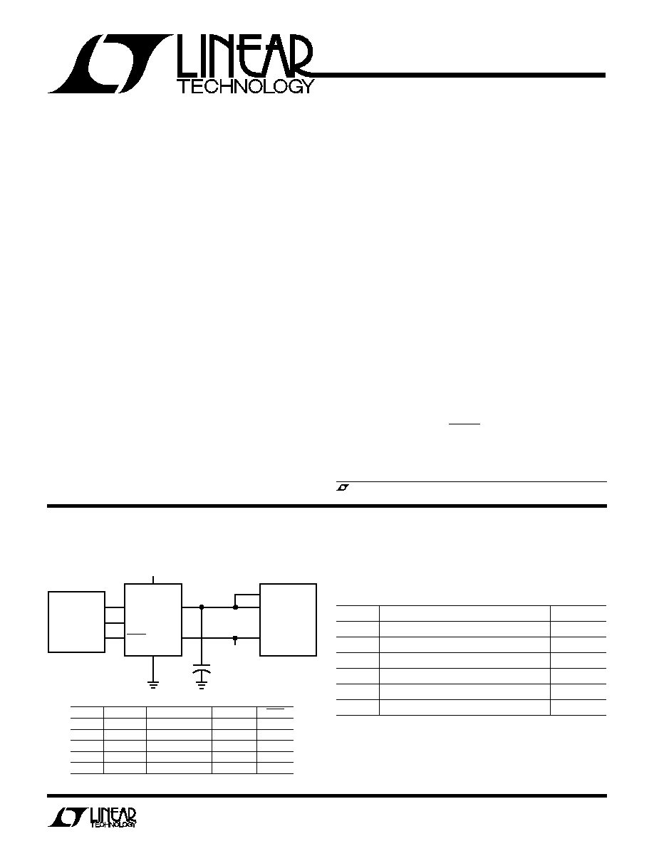
V
S
13V TO 20V
3.3V OR 5V
EN0
C
OUT
1
µ
F
TANTALUM
VPP
OUT
VPP1
VPP2
PCMCIA
CARD SLOT
V
CC
LT1312
EN1
VALID
SENSE
GND
LT1312 TA1
PCMCIA
CARD SLOT
CONTROLLER
+
TYPICAL APPLICATIO
N
U
Typical PCMCIA Single Slot VPP Driver
LT1312 TRUTH TABLE
EN0
EN1
SENSE
VPP
OUT
VALID
0
0
X
0V
1
1
0
X
12V
0
0
1
3.0V TO 3.6V
3.3V
1
0
1
4.5V TO 5.5V
5V
1
1
1
X
Hi-Z
1
X = DON'T CARE
Linear Technology PCMCIA Product Family
DEVICE
DESCRIPTION
PACKAGE
LT1312
SINGLE PCMCIA VPP DRIVER/REGULATOR
8-PIN SO
LT1313
DUAL PCMCIA VPP DRIVER/REGULATOR
16-PIN SO*
LTC
®
1314
SINGLE PCMCIA SWITCH MATRIX
14-PIN SO
LTC1315
DUAL PCMCIA SWITCH MATRIX
24-PIN SSOP
LTC1470
PROTECTED V
CC
5V/3.3V SWITCH MATRIX
8-PIN SO
LTC1472
PROTECTED V
CC
AND VPP SWITCH MATRIX
16-PIN SO*
*NARROW BODY
, LTC and LT are registered trademarks of Linear Technology Corporation.
2
LT1312
ABSOLUTE
M
AXI
M
U
M
RATINGS
W
W
W
U
PACKAGE/ORDER I
N
FOR
M
ATIO
N
W
U
U
Supply Voltage ........................................................ 22V
Digital Input Voltage ........................ 7V to (GND 0.3V)
Sense Input Voltage ......................... 7V to (GND 0.3V)
Valid Output Voltage ...................... 15V to (GND 0.3V)
Output Short-Circuit Duration .......................... Indefinite
Operating Temperature ................................ 0
°
C to 70
°
C
Junction Temperature ................................ 0
°
C to 125
°
C
Storage Temperature Range ................. 65
°
C to 150
°
C
Lead Temperature (Soldering, 10 sec).................. 300
°
C
LT1312CS8
ORDER PART
NUMBER
Consult factory for Industrial and Military grade parts.
T
JMAX
= 125
°
C,
JA
= 150
°
C/ W
1312
S8 PART MARKING
ELECTRICAL CHARACTERISTICS
SYMBOL
PARAMETER
CONDITIONS
MIN
TYP
MAX
UNITS
VPP
OUT
Output Voltage
Program to 12V, I
OUT
120mA (Note 1)
q
11.52
12.00
12.48
V
Program to 5V, I
OUT
30mA (Note 1)
q
4.75
5.00
5.25
V
Program to 3.3V, I
OUT
30mA (Note 1)
q
3.135
3.30
3.465
V
Program to 0V, I
OUT
= 300
µ
A
0.42
0.60
V
I
LKG
Output Leakage
Program to Hi-Z, 0V
VPP
OUT
12V
q
10
10
µ
A
I
S
Supply Current
Program to 0V
q
30
50
µ
A
Program to Hi-Z
q
30
50
µ
A
Program to 12V, No Load
q
230
360
µ
A
Program to 5V, No Load
q
75
120
µ
A
Program to 3.3V, No Load
q
55
90
µ
A
Program to 12V, I
OUT
= 120mA
q
126
132
mA
Program to 5V, I
OUT
= 30mA
q
31
33
mA
Program to 3.3V, I
OUT
= 30mA
q
31
33
mA
I
LIM
Current Limit
Program to 3.3V, 5V or 12V
330
500
mA
V
ENH
Enable Input High Voltage
q
2.4
V
V
ENL
Enable Input Low Voltage
q
0.4
V
I
ENH
Enable Input High Current
2.4V
V
IN
5.5V
20
50
µ
A
I
ENL
Enable Input Low Current
0V
V
IN
0.4V
0.01
1
µ
A
V
SEN5
V
CC
Sense Threshold
VPP
OUT
= 3.3V to 5V
q
3.60
4.05
4.50
V
V
SEN3
V
CC
Sense Threshold
VPP
OUT
= 5V to 3.3V
q
3.60
4.00
4.50
V
I
SEN
V
CC
Sense Input Current
V
SENSE
= 5V
38
60
µ
A
V
SENSE
= 3.3V
18
30
µ
A
V
VALID TH
VPP
VALID
Threshold Voltage
Program to 12V
q
10.5
11
11.5
V
I
VALID
VPP
VALID
Output Drive Current
Program to 12V, V
VALID
= 0.4V
1
3.3
mA
VPP
VALID
Output Leakage Current
Program to 0V, V
VALID
= 12V
0.1
10
µ
A
The
q
denotes the specifications which apply over the full operating
temperature range.
Note 1: For junction temperatures greater than 110
°
C, a minimum load
of 1mA is recommended.
V
S
= 13V to 20V, T
A
= 25
°
C, unless otherwise noted.
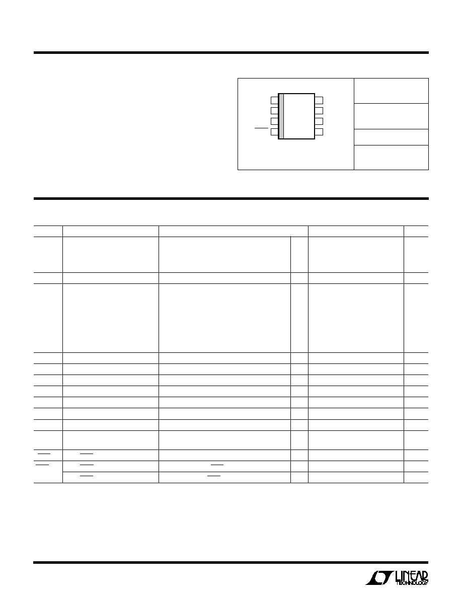
1
2
3
4
8
7
6
5
TOP VIEW
S8 PACKAGE
8-LEAD PLASTIC SO
GND
ENO
EN1
VALID
VPP
OUT
N.C.
V
S
SENSE
3
LT1312
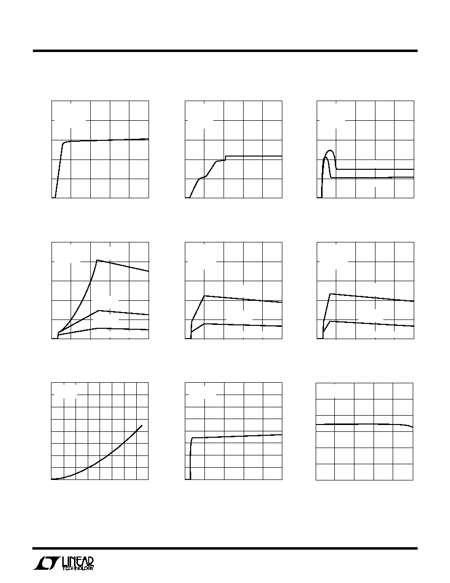
TYPICAL PERFOR
M
A
N
CE CHARACTERISTICS
U
W
OUTPUT CURRENT (mA)
0
GROUND PIN CURRENT (mA)
8
10
12
160
LT1312 G7
6
4
0
40
80
120
2
16
14
20
60
100
140
T
J
= 25°C
V
S
= 15V
SUPPLY VOLTAGE (V)
0
QUIESCENT CURRENT (µA)
30
40
50
20
LT1312 G1
20
10
0
5
10
15
25
T
J
= 25°C
EN0 = EN1= 0V
OR
EN0 = EN1= 5V
Quiescent Current (12V Mode)
Quiescent Current (0V or Hi-Z Mode)
JUNCTION TEMPERATURE (°C)
0
0
SHORT-CIRCUIT CURRENT (mA) 100
200
300
400
500
600
25
50
75
100
LT1312 G9
125
V
S
= 15V
VPP
OUT
= 0V
Current Limit
SUPPLY VOLTAGE (V)
0
GROUND CURRENT (mA)
1.5
2.0
2.5
20
LT1312 G6
1.0
0.5
0
5
10
15
25
T
J
= 25°C
EN0 = 0V
EN1 = 5V
V
SENSE
= 3.3V
R
L
= 110
I
L
= 30mA*
*FOR VPP
OUT
= 3.3V
R
L
= 330
I
L
= 10mA*
Ground Pin Current (3.3V Mode)
SUPPLY VOLTAGE (V)
0
QUIESCENT CURRENT (µA)
150
200
250
20
LT1312 G3
100
50
0
5
10
15
25
T
J
= 25°C
EN0 = 0V
EN1 = 5V
R
L
=
V
SENSE
= 5V
V
SENSE
= 3.3V
Quiescent Current (3.3V/5V Mode)
SUPPLY VOLTAGE (V)
0
QUIESCENT CURRENT (µA)
300
400
500
20
LT1312 G2
200
100
0
5
10
15
25
T
J
= 25°C
EN0 = 5V
EN1 = 0V
R
L
=
Ground Pin Current
SUPPLY VOLTAGE (V)
0
GROUND CURRENT (mA)
6
8
10
20
LT1312 G4
4
2
0
5
10
15
25
T
J
= 25°C
EN0 = 5V
EN1 = 0V
R
L
= 100
I
L
= 120mA*
R
L
= 200
I
L
= 60mA*
*FOR VPP
OUT
= 12V
R
L
= 400
I
L
= 30mA*
Ground Pin Current (12V Mode)
Ground Pin Current (5V Mode)
SUPPLY VOLTAGE (V)
0
GROUND CURRENT (mA)
1.5
2.0
2.5
20
LT1312 G5
1.0
0.5
0
5
10
15
25
T
J
= 25°C
EN0 = 0V
EN1 = 5V
V
SENSE
= 5V
R
L
= 167
I
L
= 30mA*
*FOR VPP
OUT
= 5V
R
L
= 500
I
L
= 10mA*
Current Limit
INPUT VOLTAGE (V)
0
SHORT-CIRCUIT CURRENT (mA)
300
400
500
15
25
LT1312 G8
200
100
0
5
10
20
600
700
800
T
J
= 25°C
VPP
OUT
= 0V
4
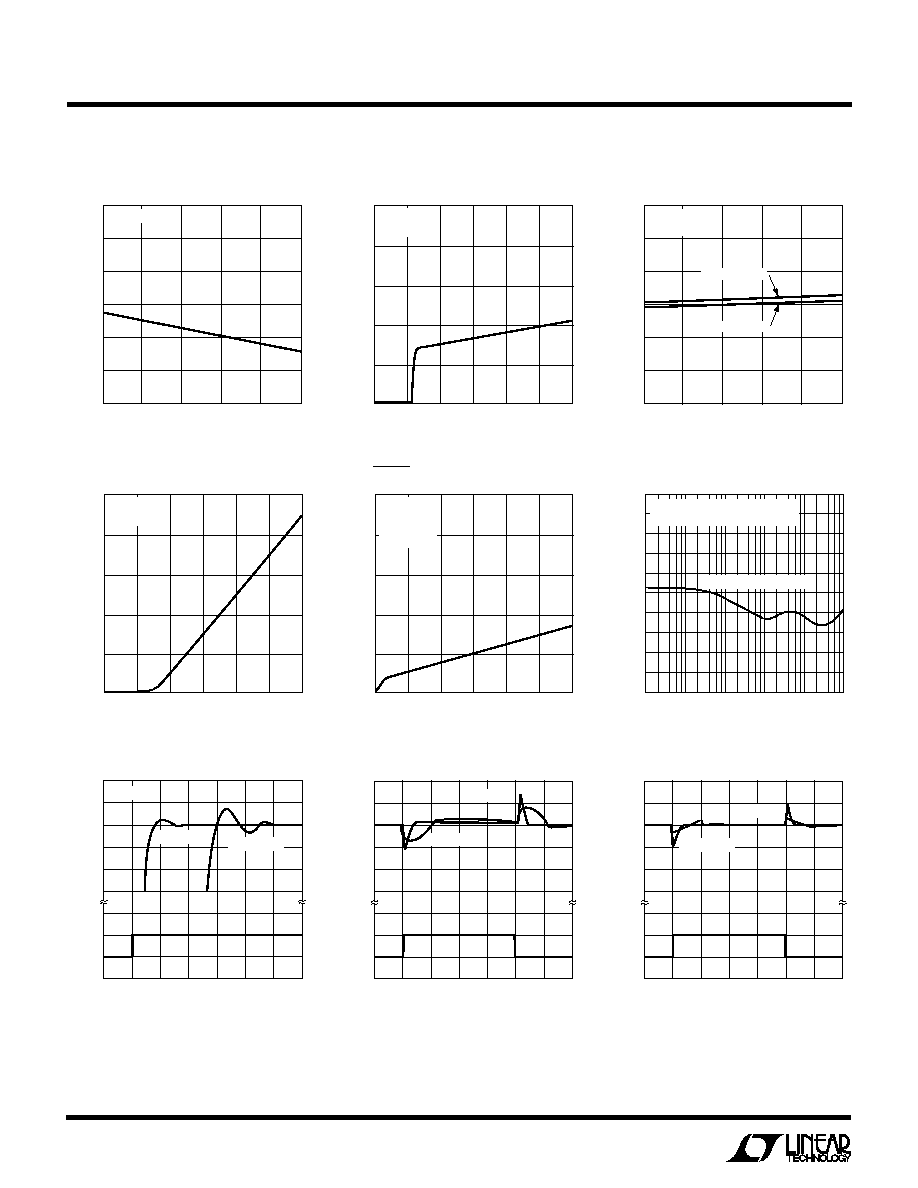
LT1312
TYPICAL PERFOR
M
A
N
CE CHARACTERISTICS
U
W
V
CC
Sense Input Current
JUNCTION TEMPERATURE (°C)
0
0
INPUT THRESHOLD VOLTAGE (V) 0.5
1.0
1.5
2.0
2.5
3.0
25
50
75
100
LT1312 G10
125
V
S
= 15V
12V Turn-On Waveform
Enable Input Current
Enable Input Threshold Voltage
ENABLE INPUT VOLTAGE (V)
0
0
ENABLE INPUT CURRENT (µA)
10
20
30
40
50
1
2
3
4
LT1312 G11
5
6
T
J
= 25°C
V
S
= 15V
V
CC
Sense Threshold Voltage
JUNCTION TEMPERATURE (°C)
0
2.5
V
CC
SENSE THRESHOLD VOLTAGES (V) 3.0
3.5
4.0
4.5
5.0
5.5
25
50
75
100
LT1312 G12
125
T
J
= 25°C
V
S
= 15V
SWITCH TO 5V
SWITCH TO 3.3V
ENABLE INPUT VOLTAGE (V)
0
0
V
CC
SENSE INPUT CURRENT (µA)
10
20
30
40
50
1
2
3
4
LT1312 G13
5
6
T
J
= 25°C
V
S
= 15V
VALID Output Voltage
VALID OUTPUT CURRENT (mA)
0
0
VALID OUTPUT VOLTAGE (V) 0.2
0.4
0.6
0.8
1.0
0.5
1.0
1.5
2.0
LT1312 G14
2.5
3.0
T
J
= 25°C
V
S
= 15V
EN0 = 5V
EN1 = 0V
Ripple Rejection (12V)
FREQUENCY (Hz)
10
RIPPLE REJECTION RATIO (dB)
100
1k
10k
100k
1M
LT1312 G15
100
80
60
40
20
0
T
J
= 25°C, 12V MODE
V
S
= 15V
+
100mV
RMS
RIPPLE
C
OUT
= 1µF TANTALUM
TIME (ms)
0.2
0
0.2
0.4
0.6
0.8
1.0
1.2
OUTPUT VOLTAGE (V)
EN0 INPUT (V)
0
11.6
12.4
LT1312 G16
5
11.8
12.0
12.2
C
OUT
= 1µF
C
OUT
= 10µF
V
S
= 15V
Load Transient Response (12V)
TIME (ms)
0.1
0
0.1
0.2
0.3
0.4
0.5
0.6
OUTPUT VOLTAGE
CHANGE (V)
LOAD
CURRENT (mA)
50
0.4
0.4
LT1312 G18
100
0.2
0
0.2
C
OUT
= 1µF
C
OUT
= 10µF
Line Transient Response (12V)
TIME (ms)
0.1
0
0.1
0.2
0.3
0.4
0.5
0.6
OUTPUT VOLTAGE
CHANGE (mV)
SUPPLY
VOLTAGE (V)
13
40
40
LT1312 G17
15
20
0
20
C
OUT
= 1µF
C
OUT
= 10µF
5
LT1312
at 2.4V. The input thresholds are compatible with CMOS
controllers and can be driven from either 5V or 3.3V
CMOS logic. ESD protection diodes limit input excursions
to 0.6V below ground.
VALID Output Pin: This pin is an open-collector NPN
output which is driven low when the VPP
OUT
pin is in
regulation, i.e., when it is above 11V. An external 51k pull-
up resistor is connected between this output and the same
5V or 3.3V logic supply powering the PCMCIA compatible
control logic.
V
CC
Sense Pin: A built-in comparator and 4V reference
automatically switches the VPP
OUT
from 5V to 3.3V de-
pending upon the voltage sensed at the PCMCIA card
socket V
CC
pin. The input current for this pin is approxi-
mately 30
µ
A. For 5V only operation, connect the Sense pin
directly to ground. An ESD protection diode limits the
input voltage to 0.6V below ground.
PI
N
FU
N
CTIO
N
S
U
U
U
Supply Pin: Power is supplied to the device through the
supply pin. The supply pin should be bypassed to ground
if the device is more than 6 inches away from the main
supply capacitor. A bypass capacitor in the range of 0.1
µ
F
to 1
µ
F is sufficient. The supply voltage to the LT1312 can
be loosely regulated between 13V and 20V. See Applica-
tions Information section for more detail.
VPP
OUT
Pin: This regulated output supplies power to the
PCMCIA card VPP pins which are typically tied together
at the card socket. The VPP
OUT
output is current limited
to approximately 330mA. Thermal shutdown provides a
second level of protection. A 1
µ
F to 10
µ
F tantalum output
capacitor is recommended. See Applications Informa-
tion section for more detail on output capacitor consid-
erations.
Input Enable Pins: The two digital input pins are high
impedance inputs with approximately 20
µ
A input current
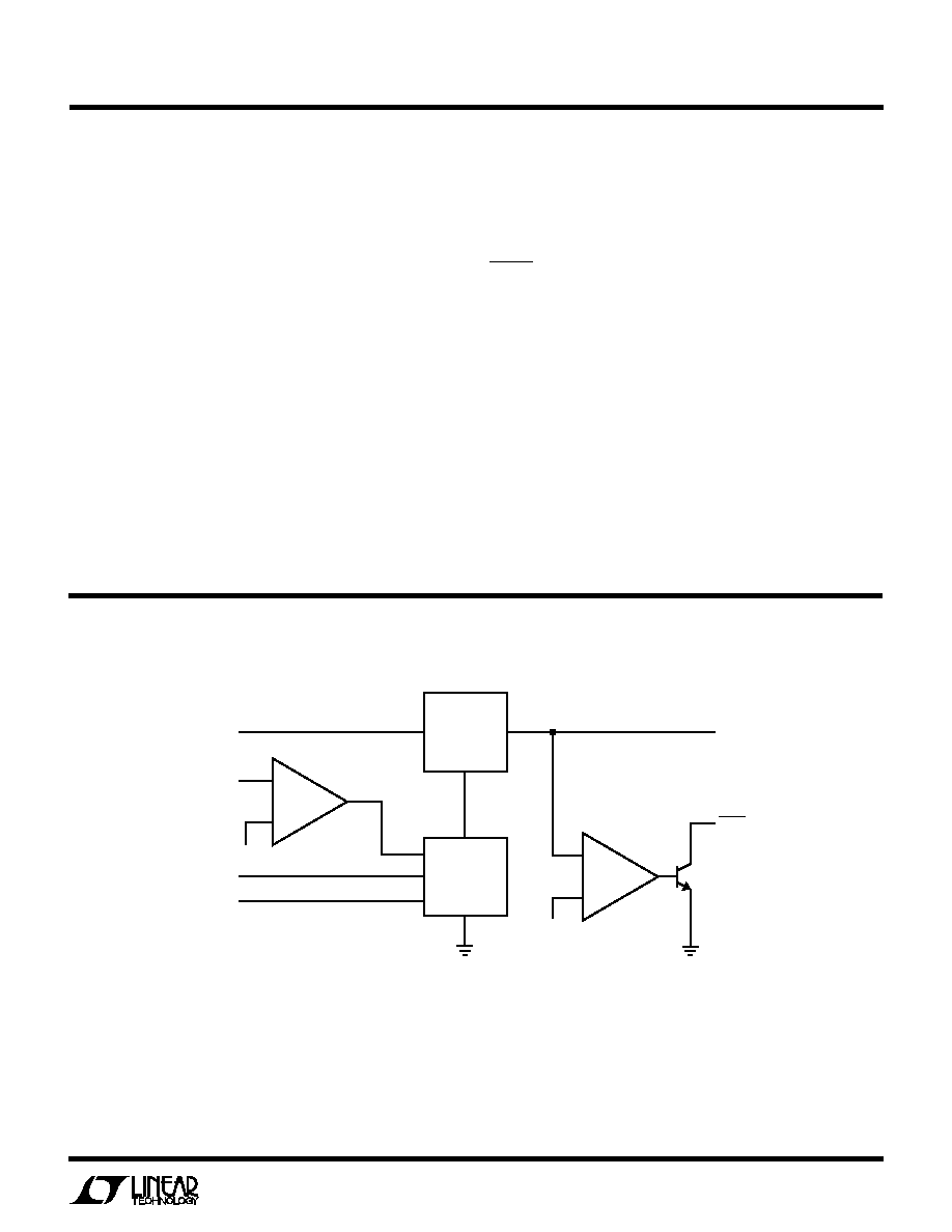
BLOCK DIAGRA
M
W
+
+
VPP
OUT
V
CC
SENSE
V
S
EN0
EN1
VALID
LT1312 BD
11V
LOW DROPOUT
LINEAR
REGULATOR
VOLTAGE
LOGIC CONTROL
4V