 | ÐлекÑÑоннÑй компоненÑ: LT1330 | СкаÑаÑÑ:  PDF PDF  ZIP ZIP |
Äîêóìåíòàöèÿ è îïèñàíèÿ www.docs.chipfind.ru
1
LT1330
5V RS232 Transceiver with
3V Logic Interface and One
Receiver Active in Shutdown
R
1330 TA02
U
S
A
O
PPLICATI
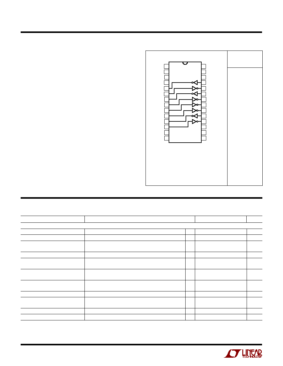
Output Waveforms
RECEIVER
OUTPUT
V
L
= 3V
C
L
= 50pF
DRIVER
OUTPUT
R
L
= 3k
C
L
= 2500pF
s
Notebook Computers
s
Palmtop Computers
U
A
O
PPLICATI
TYPICAL
INPUT
s
3V Logic Interface
s
ESD Protection over
±
10kV
s
Uses Small Capacitors: 0.1
µ
F, 0.2
µ
F, 1.0
µ
F
s
One Low Power Receiver Remains Active While in
Shutdown
s
Pin Compatible with LT1137A and LT1237
s
120kBaud Operation for R
L
= 3k, C
L
= 2500pF
s
250kBaud Operation for R
L
= 3k, C
L
= 1000pF
s
CMOS Comparable Low Power: 30mW
s
Easy PC Layout--Flowthrough Architecture
s
Rugged Bipolar Design
s
Outputs Assume a High Impedance State When Off
or Powered Down
s
Absolutely No Latchup
s
60
µ
A Supply Current in Shutdown
s
Available in SO and SSOP Packages
D
U
ESCRIPTIO
S
FEATURE
, LTC and LT are registered trademarks of Linear Technology Corporation.
The LT
®
1330 is a three driver, five receiver RS232 trans-
ceiver with low supply current. Designed to interface with
new 3V logic, the LT1330 operates with both a 5V power
supply and a 3V logic power supply. The chip may be shut
down to micropower operation with one receiver remain-
ing active to monitor RS232 inputs such as ring detect
from a modem.
The LT1330 is fully compliant with all EIA RS232 specifi-
cations. Additionally, the RS232 line input and output pins
are resilient to multiple
±
10kV ESD strikes. This eliminates
the need for costly TransZorbs
®
on line pins for the RS232
part.
The LT1330 operates to 120kbaud even driving high
capacitive loads. During shutdown, driver and receiver
outputs are at a high impedance state allowing devices to
be paralleled.
TransZorb is a registered trademark of General Instruments, GSI
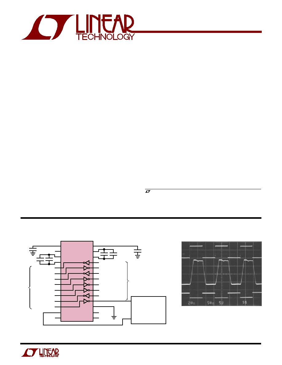
1330 TA01
5V V
CC
1.0
µ
F
2
×
0.1
µ
F
0.1
µ
F
TO
LINE
LT1330
1
2
3
4
5
6
7
8
9
10
11
12
13
14
DRIVER 1 OUT
RX1 IN
DRIVER 2 OUT
RX2 IN
RX3 IN
RX4 IN
DRIVER 3 OUT
RX5 IN (LOW-Q)
ON/OFF
3V V
L
28
27
26
25
24
23
22
21
20
19
18
17
16
15
2
×
0.1
µ
F
DRIVER 1 IN
RX1 OUT
DRIVER 2 IN
RX2 OUT
RX3 OUT
RX4 OUT
DRIVER 3 IN
RX5 OUT (LOW-Q)
GND
DRIVER
DISABLE
RING DETECT IN
SHUTDOWN
CONTROL OUT
µ
CONTROLLER OR
µ
PROCESSOR
TO LOGIC
V
V
+
2
LT1330
(Note 1)
Supply Voltage (V
CC
) ................................................ 6V
Supply Voltage (V
L
) .................................................. 6V
V
+
........................................................................ 13.2V
V
...................................................................... 13.2V
Input Voltage
Driver ........................................................... V
to V
+
Receiver ................................................ 30V to 30V
Output Voltage
Driver .................................................... 30V to 30V
Receiver ...................................... 0.3V to V
L
+ 0.3V
Short-Circuit Duration
V
+
................................................................... 30 sec
V
................................................................... 30 sec
Driver Output .............................................. Indefinite
Receiver Output .......................................... Indefinite
Operating Temperature Range
LT1330I ............................................. 40
°
C to 85
°
C
LT1330C ................................................. 0
°
C to 70
°
C
Storage Temperature Range ................ 65
°
C to 150
°
C
Lead Temperature (Soldering, 10 sec)................. 300
°
C
A
U
G
W
A
W
U
W
A
R
BSOLUTE
XI
TI
S
W
U
U
PACKAGE/ORDER I FOR ATIO
ORDER PART
NUMBER
ELECTRICAL C
C
HARA TERISTICS
(Note 2)
Consult factory for Military grade parts.
LT1330CG
LT1330CJW
LT1330CNW
LT1330CSW
LT1330IJW
T
JMAX
= 150
°
C,
JA
= 96
°
C/ W (G)
T
JMAX
= 150
°
C,
JA
= 62
°
C/ W (JW)
T
JMAX
= 150
°
C,
JA
= 56
°
C/ W (NW)
T
JMAX
= 150
°
C,
JA
= 85
°
C/ W (SW)
1
2
3
4
5
6
7
8
9
10
11
12
13
14
V
+
5V V
CC
C1
+
C1
DR1 OUT
RX1 IN
DR2 OUT
RX2 IN
RX3 IN
RX4 IN
DR3 OUT
RX5 IN
(LOW-Q)
ON/OFF
3V V
L
28
27
26
25
24
23
22
21
20
19
18
17
16
15
V
C2
C2
+
DR1 IN
RX1 OUT
DR2 IN
RX2 OUT
RX3 OUT
RX4 OUT
DR3 IN
RX5 OUT
(LOW-Q)
GND
DRIVER
DISABLE
NC
JW PACKAGE
28-LEAD (WIDE) CERDIP
NW PACKAGE
28-LEAD (WIDE) PDIP
TOP VIEW
SW PACKAGE
28-LEAD (WIDE) PLASTIC SO
G PACKAGE
28-LEAD PLASTIC SSOP
PARAMETER
CONDITIONS
MIN
TYP
MAX
UNITS
Power Supply Generator
V
+
Output
7.9
V
V
Output
7
V
Supply Current (V
CC
)
T
A
= 25
°
C (Note 3)
6
12
mA
q
6
14
mA
Supply Current (V
L
)
(Note 4)
0.1
1
mA
Supply Current When OFF (V
CC
)
Shutdown (Note 5)
q
0.06
0.15
mA
Driver Disable
3.00
mA
Supply Rise Time
C1 = C2 = 0.2
µ
F,
0.2
ms
Shutdown to Turn-On
C
+
= 1.0
µ
F, C
= 0.1
µ
F
ON/OFF Pin Thresholds
Input Low Level (Device Shutdown)
q
0.8
1.4
V
Input High Level (Device Enabled)
q
1.4
2.4
V
ON/OFF Pin Current
0V
V
ON/OFF
5V
q
15
80
µ
A
DRIVER DISABLE Pin Thresholds
Input Low Level (Drivers Enabled)
q
0.8
1.4
V
Input High Level (Drivers Disabled)
q
1.4
2.4
V
DRIVER DISABLE Pin Current
0V
V
DRIVER DISABLE
5V
q
10
500
µ
A
Oscillator Frequency
Driver Outputs Loaded R
L
= 3k
130
kHz
3
LT1330
PARAMETER
CONDITIONS
MIN
TYP
MAX
UNITS
Any Driver
Output Voltage Swing
Load = 3k to GND
Positive
q
5.0
7.5
V
Negative
q
6.3
5.0
V
Logic Input Voltage Level
Input Low Level (V
OUT
= High)
q
1.4
0.8
V
Input High Level (V
OUT
= Low)
q
2.0
1.4
V
Logic Input Current
0.8V
V
IN
2V
q
5
20
µ
A
Output Short-Circuit Current
V
OUT
= 0V
±
9
17
mA
Output Leakage Current
Shutdown V
OUT
=
±
30V (Note 5)
q
10
100
µ
A
Data Rate (Note 8)
R
L
= 3k, C
L
= 2500pF
120
kBaud
R
L
= 3k, C
L
= 1000pF
250
kBaud
Slew Rate
R
L
= 3k, C
L
= 51pF
15
30
V/
µ
s
R
L
= 3k, C
L
= 2500pF
4
15
V/
µ
s
Propagation Delay
Output Transition t
HL
High to Low (Note 6)
0.6
1.3
µ
s
Output Transition t
LH
Low to High
0.5
1.3
µ
s
Any Receiver
Input Voltage Thresholds
Input Low Threshold (V
OUT
= High)
0.8
1.3
V
Input High Threshold (V
OUT
= Low)
1.7
2.4
V
Hysteresis
q
0.1
0.4
1.0
V
Input Resistance
V
IN
=
±
10V
3
5
7
k
Output Leakage Current
Shutdown (Note 5) 0
V
OUT
V
CC
q
1
10
µ
A
Receivers 1, 2, 3, 4
Output Voltage
Output Low, I
OUT
= 1.6mA
q
0.2
0.4
V
Output High, I
OUT
= 160
µ
A (V
L
= 3V)
q
2.7
2.9
V
Output Short-Circuit Current
Sinking Current, V
OUT
= V
CC
10
20
mA
Sourcing Current, V
OUT
= 0V
10
20
mA
Propagation Delay
Output Transition t
HL
High to Low (Note 7)
250
600
ns
Output Transition t
LH
Low to High
350
600
ns
Receiver 5 (LOW Q-Current RX)
Output Voltage
Output Low, I
OUT
= 500
µ
A
q
0.2
0.4
V
Output High, I
OUT
= 160
µ
A (V
L
= 3V)
q
2.7
2.9
V
Output Short-Circuit Current
Sinking Current, V
OUT
= V
CC
2
4
mA
Sourcing Current, V
OUT
= 0V
2
4
mA
Propagation Delay
Output Transition t
HL
High to Low (Note 7)
1
3
µ
s
Output Transition t
LH
Low to High
1
3
µ
s
ELECTRICAL C
C
HARA TERISTICS
(Note 2)
The
q
denotes specifications which apply over the operating temperature
range (0
°
C
T
A
70
°
C for commercial grade, and 40
°
C
T
A
85
°
C for
industrial grade).
Note 1: Absolute Maximum Ratings are those values beyond which the life
of the device may be impaired.
Note 2: Testing done at V
CC
= 5V and V
ON/OFF
= 3V.
Note 3: Supply current is measured as the average over several charge
pump burst cycles. C
+
= 1.0
µ
F, C
= 0.1
µ
F, C1 = C2 = 0.2
µ
F. All outputs
are open, with all driver inputs tied high.
Note 4: V
L
supply current is measured with all receiver outputs low.
Note 5: Measurements in shutdown are performed with V
ON/OFF
0.1V.
Supply current measurements using driver disable are performed with
V
DRIVER DISABLE
3V.
Note 6: For driver delay measurements, R
L
= 3k and C
L
= 51pF. Trigger
points are set between the driver's input logic threshold and the output
transition to the zero crossing (t
HL
= 1.4V to 0V and t
LH
= 1.4V to 0V).
Note 7: For receiver delay measurements, C
L
= 51pF. Trigger points are
set between the receiver's input logic threshold and the output transition
to standard TTL/CMOS logic threshold (t
HL
= 1.3V to 2.4V and t
LH
= 1.7V
to 0.8V).
Note 8: Data rate operation guaranteed by slew rate, short-circuit current
and propagation delay tests.
4
LT1330
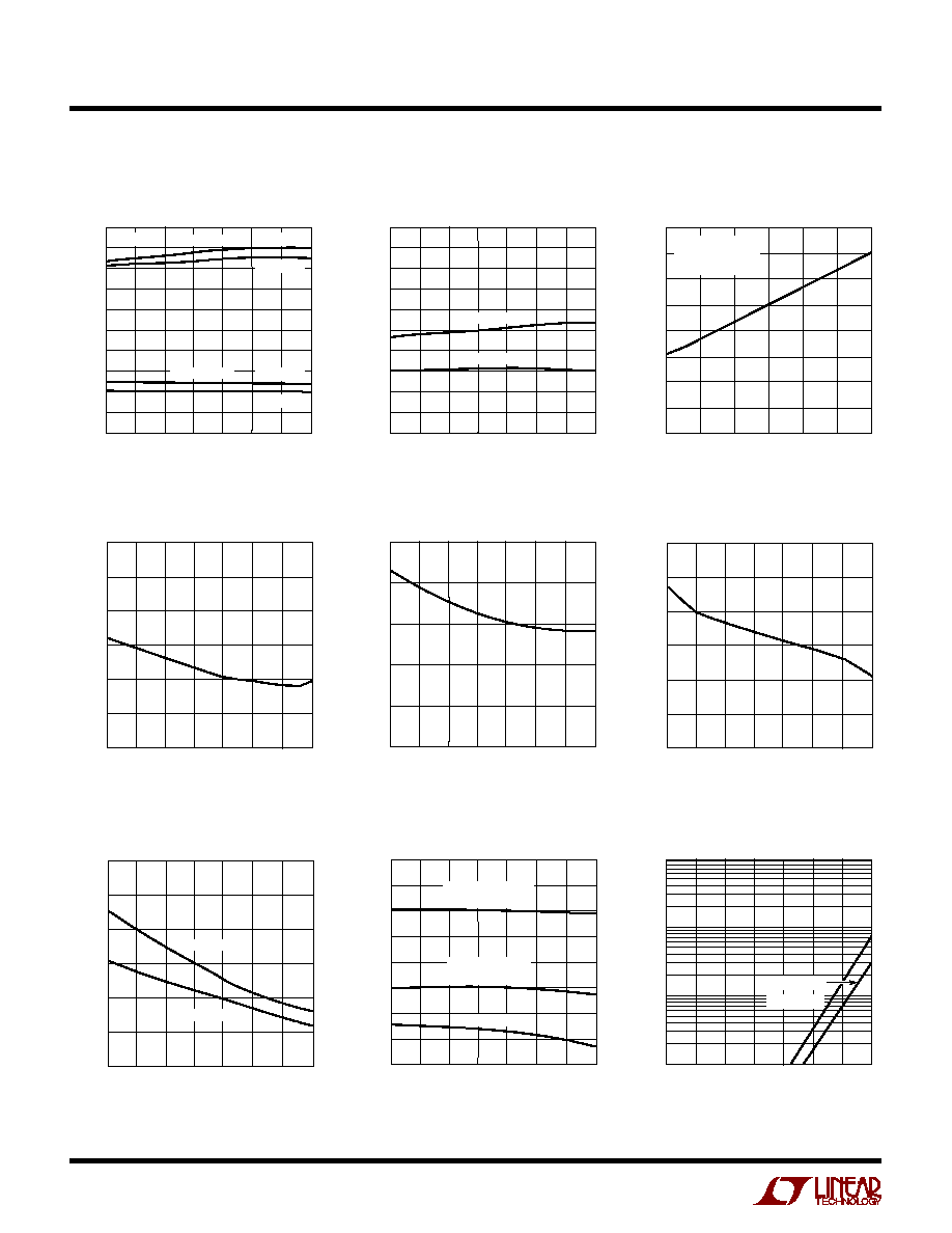
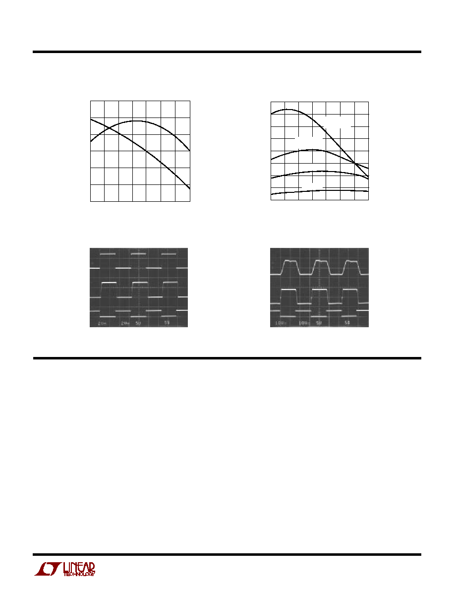
C
C
HARA TERISTICS
U
W
A
TYPICAL PERFOR
CE
Driver Output Voltage
Receiver Input Thresholds
Supply Current vs Data Rate
DRIVER DISABLE Threshold
ON/OFF Thresholds
V
CC
Supply Current
Driver Leakage in Shutdown
V
CC
Supply Current in
Driver Disable
TEMPERATURE (°C)
55
10
DRIVER OUTPUT VOLTAGE (V)
8
4
2
0
10
4
0
50
75
1330 G01
6
6
8
2
25
25
100
125
OUTPUT HIGH
OUTPUT LOW
R
L
= 3k
V
CC
= 5V
V
CC
= 4.5V
V
CC
= 4.5V
V
CC
= 5V
TEMPERATURE (°C)
55
0.50
THRESHOLD VOLTAGE (V)
0.75
1.25
1.50
1.75
3.00
2.25
0
50
75
1330 G02
1.00
2.50
2.75
2.00
25
25
100
125
INPUT HIGH
INPUT LOW
DATA RATE (kBAUD)
0
0
SUPPLY CURRENT (mA)
20
30
40
60
25
50
125
150
1330 G03
70
80
50
10
75
100
3DRIVERS ACTIVE
R
L
= 3k
C
L
= 2500pF
TEMPERATURE (°C)
55
0
SUPPLY CURRENT (mA)
2
5
0
50
75
1330 G05
1
4
3
25
25
100
125
TEMPERATURE (°C)
0
SUPPLY CURRENT (mA)
10
15
20
30
1330 G08
35
40
25
5
3DRIVERS LOADED
R
L
= 3k
55
0
50
75
25
25
100
125
1DRIVER LOADED
R
L
= 3k
NO LOAD
TEMPERATURE (°C)
55
SUPPLY CURRENT (
µ
A)
100
125
150
25
75
1330 G04
75
50
25
0
50
100
125
25
0
TEMPERATURE (°C)
55
THRESHOLD VOLTAGE (V)
2.0
2.5
3.0
25
75
1330 G06
1.5
1.0
25
0
50
100
125
0.5
0
TEMPERATURE (°C)
0.1
LEAKAGE CURRENT (
µ
A)
10
100
1330 G09
1
55
0
50
75
25
25
100
125
V
OUT
= 30V
V
OUT
= 30V
TEMPERATURE (°C)
55
THRESHOLD VOLTAGE (V)
2.0
2.5
3.0
25
75
1330 G07
1.5
1.0
25
0
50
100
125
0.5
0
ON THRESHOLD
OFF THRESHOLD
V
CC
Supply Current in Shutdown
5
LT1330
C
C
HARA TERISTICS
U
W
A
TYPICAL PERFOR
CE
V
CC
: 5V Input Supply Pin. This pin should be decoupled
with a 0.1
µ
F ceramic capacitor close to the package pin.
Insufficient supply bypassing can result in low output
drive levels and erratic charge pump operation.
V
L
: 3V Logic Supply Pin for all RS232 Receivers. Like V
CC
,
the V
L
input should be decoupled with a 0.1
µ
F ceramic
capacitor. This pin may also be connected to 5V.
GND: Ground Pin.
ON/OFF: TTL/CMOS Compatible Operating Mode Control.
A logic low puts the device in the low power shutdown
mode. All three drivers and four receivers (RX1, RX2, RX3,
and RX4) assume a high impedance output state in shut-
down. Only receiver RX5 remains active while the trans-
ceiver is in shutdown. The transceiver consumes only
PI FU CTIO S
U
U
U
60
µ
A of supply current while in shutdown. A logic high
fully enables the transceiver.
DRIVER DISABLE: This pin provides an alternate control
for the charge pump and RS232 drivers. A logic high on
this pin shuts down the charge pump and places all driver
outputs in a high impedance state. All five receivers remain
active under these conditions. Floating the driver disable
pin or driving it to a logic low level fully enables the
transceiver. A logic low on the ON/OFF pin supersedes the
state of the DRIVER DISABLE pin. Supply current drops to
3mA when in driver disable mode.
V
+
: Positive Supply Output. V
+
2V
CC
1.5V. This pin
requires an external charge storage capacitor, C
1.0
µ
F,
tied to ground or 5V. Larger value capacitors may be used
Receiver Output Waveforms
RX5 OUTPUT
C
L
= 50pF
Receiver Short-Circuit Current
Driver Short-Circuit Current
TEMPERATURE (°C)
55
0
SHORT-CIRCUIT CURRENT (mA)
15
40
0
50
75
1330 G11
10
35
25
25
25
100
125
30
20
5
RX1 TO RX4
I
SC+
RX1 TO RX4
I
SC
RX5 I
SC+
RX5 I
SC
TEMPERATURE (
°
C)
55
SHORT-CIRCUIT CURRENT (mA)
20
25
30
25
75
1330 G10
15
10
25
0
50
100
125
5
0
I
SC
+
I
SC
V
L
= 3V
INPUT
1330 G13
INPUT
DRIVER OUTPUT
R
L
= 3k
DRIVER OUTPUT
R
L
= 3k
C
L
= 2500pF
RX1 TO RX4
OUTPUT
C
L
= 50pF
1330 G12
Driver Output Waveforms