 | ÐлекÑÑоннÑй компоненÑ: LT1332 | СкаÑаÑÑ:  PDF PDF  ZIP ZIP |
Äîêóìåíòàöèÿ è îïèñàíèÿ www.docs.chipfind.ru
1
LT1332
Wide Supply Range
Low Power RS232 Transceiver with
12V VPP Output for Flash Memory
S
FEATURE
s
Generates Full RS232 Signal Levels from 3V Supply
s
12V VPP Output Available for Flash Memory
s
Useful with a Wide Variety of Switching Regulators
s
Low Supply Current: I(V
CC
) = 1mA
s
Wide Supply Range: 2V
V
CC
6V
s
ESD Protection Over
±
10kV
s
Operates to 120k Baud
s
Outputs Assume a High Impedance State When Off
or Powered Down
s
One
µ
Power Receiver Remains Active While in
SHUTDOWN
s
Flowthrough Architecture Eases PC Board Layout
s
40
µ
A Supply Current in SHUTDOWN
s
Absolutely No Latch-Up
s
Available in SO and SSOP Packages
U
S
A
O
PPLICATI
s
Notebook and Palmtop Computers
s
Mouse Driver Circuits
D
U
ESCRIPTIO
The LT1332 is a 3-driver/5-receiver RS232 transceiver,
designed to be used in conjunction with a switching
regulator. The LT1332 shares the regulator's positive
output, while charge is capacitively pumped from the
regulator's switch pin to the negative supply. Schottky
rectifiers built into the LT1332 simplify the charge
pump design.
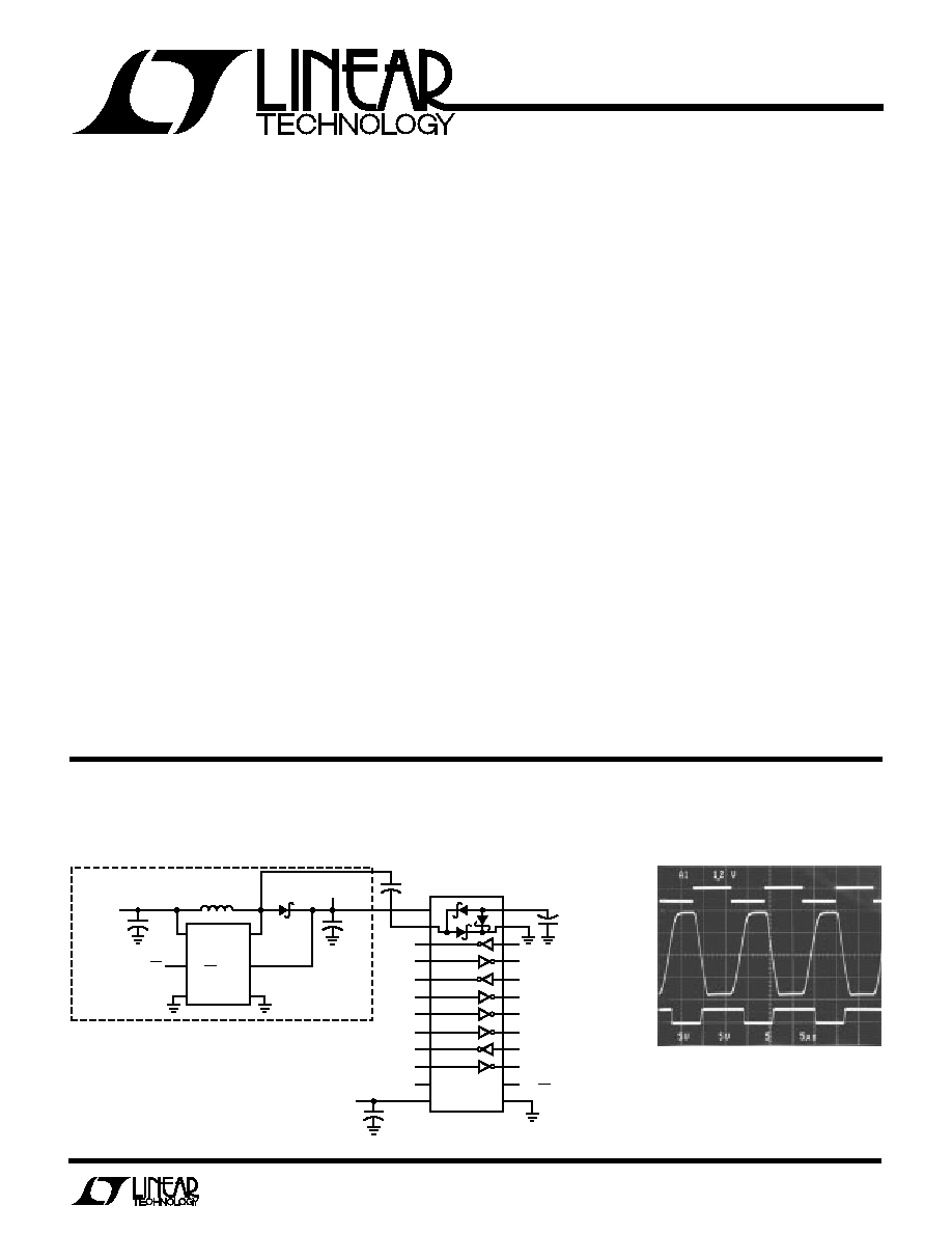
The LT1332/LT1109A combination shown below gener-
ates fully compliant RS232 signal levels from as little as 2V
of input supply. The switcher can deliver greater than
100mA of output current, making the LT1332 an excellent
choice for mouse driver circuits.
Advanced driver output stages operate up to 120k baud
while driving heavy capacitive loads. New ESD structures
on chip make the LT1332 resilient to multiple
±
10kV
strikes, eliminating costly transient suppressors.
A shutdown pin disables the transceiver except for one
receiver which remains active for detecting incoming
RS232 signals. When shut down, the disabled drivers and
receivers assume high impedance output states.
U
A
O
PPLICATI
TYPICAL
LT1332 · TA01
22
µ
F*
LT1332
1
2
3
4
5
6
7
8
9
10
11
12
24
23
22
21
20
19
18
17
16
15
14
13
SWITCHER
V
IN
2 AA
BATTERIES
UP TO 6V
V
V
+
1
µ
F
10
µ
F
+
C
12V VPP
OUTPUT
22
µ
F*
STANDARD FLASH MEMORY VPP GENERATOR
L1**
33
µ
H
0.1
µ
F
3V
RS232
V
CC
ON/OFF
RS232
ON/OFF
RS232
SIDE
LOGIC
SIDE
NC
+
LT1109A-12
V
IN
SW
ON/OFF
SENSE
GND
PGND
SW
*
**
AVX TAJE226K035
SUMIDA CD54-330N (708-956-0666)
MBRS130T3
LT1332 Powered from an LT1109A Micropower Switching Regulator
Configured for Flash Memory
Output Waveforms
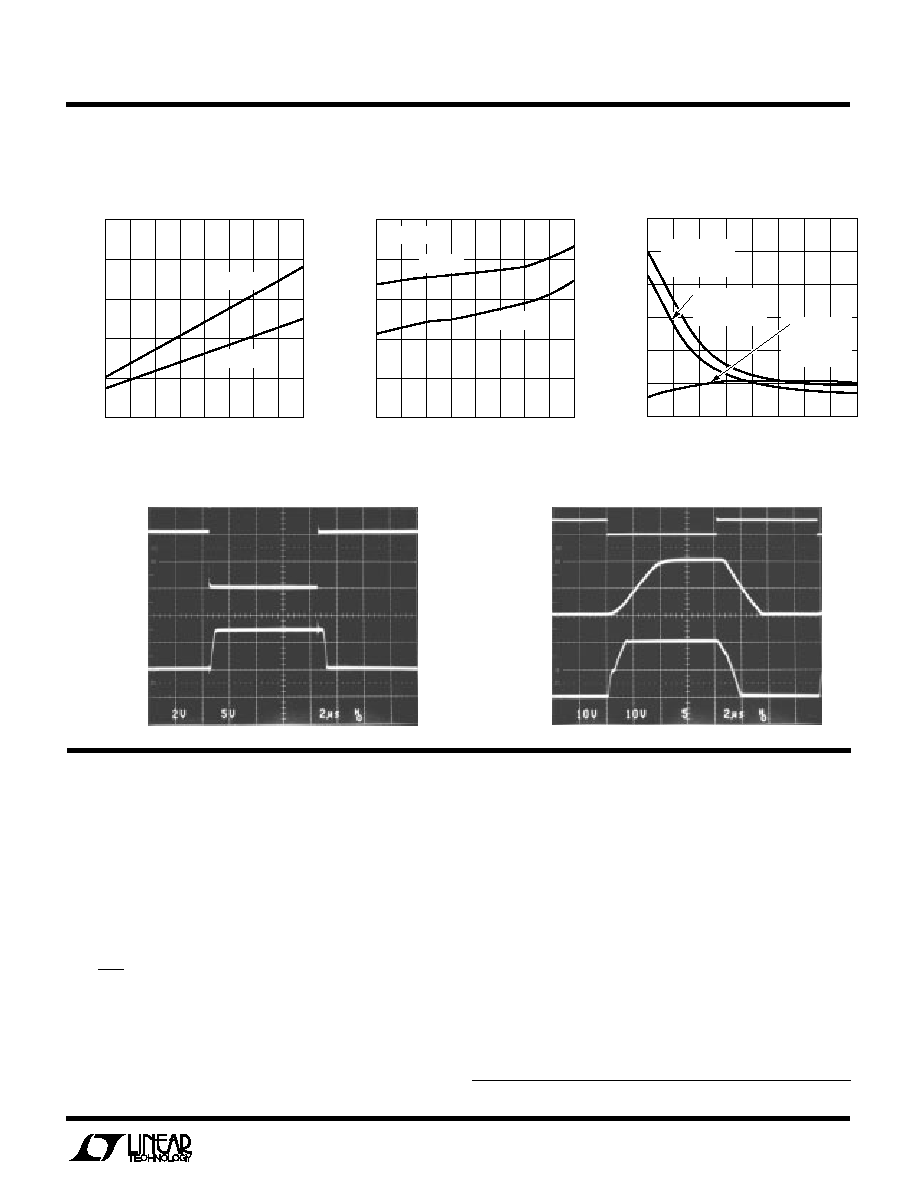
DRIVER
OUTPUT
R
L
= 3k
C
L
= 2500pF
RECEIVER
OUTPUT
C
L
= 50pF
LT1332 · TA02
DRIVER
INPUT
2
LT1332
A
U
G
W
A
W
U
W
A
R
BSOLUTE
XI
TI
S
Supply Voltage (V
CC
) ................................................ 6V
V
+
........................................................................ 13.2V
V
...................................................................... 13.2V
C
......................................................................... 15V
Input Voltage
Driver .......................................................... V
+
to V
Receiver ................................................ 30V to 30V
Output Voltage
Driver .................................................... 30V to 30V
Receiver .................................... 0.3V to V
CC
+ 0.3V
(Note 1)
Short Circuit Duration
V
+
................................................................... 30 sec
V
................................................................... 30 sec
Driver Output .............................................. Indefinite
Receiver Output .......................................... Indefinite
Operating Temperature Range .................... 0
°
C to 70
°
C
Storage Temperature Range ................ 65
°
C to 150
°
C
Lead Temperature (Soldering, 10 sec) ................. 300
°
C
W
U
U
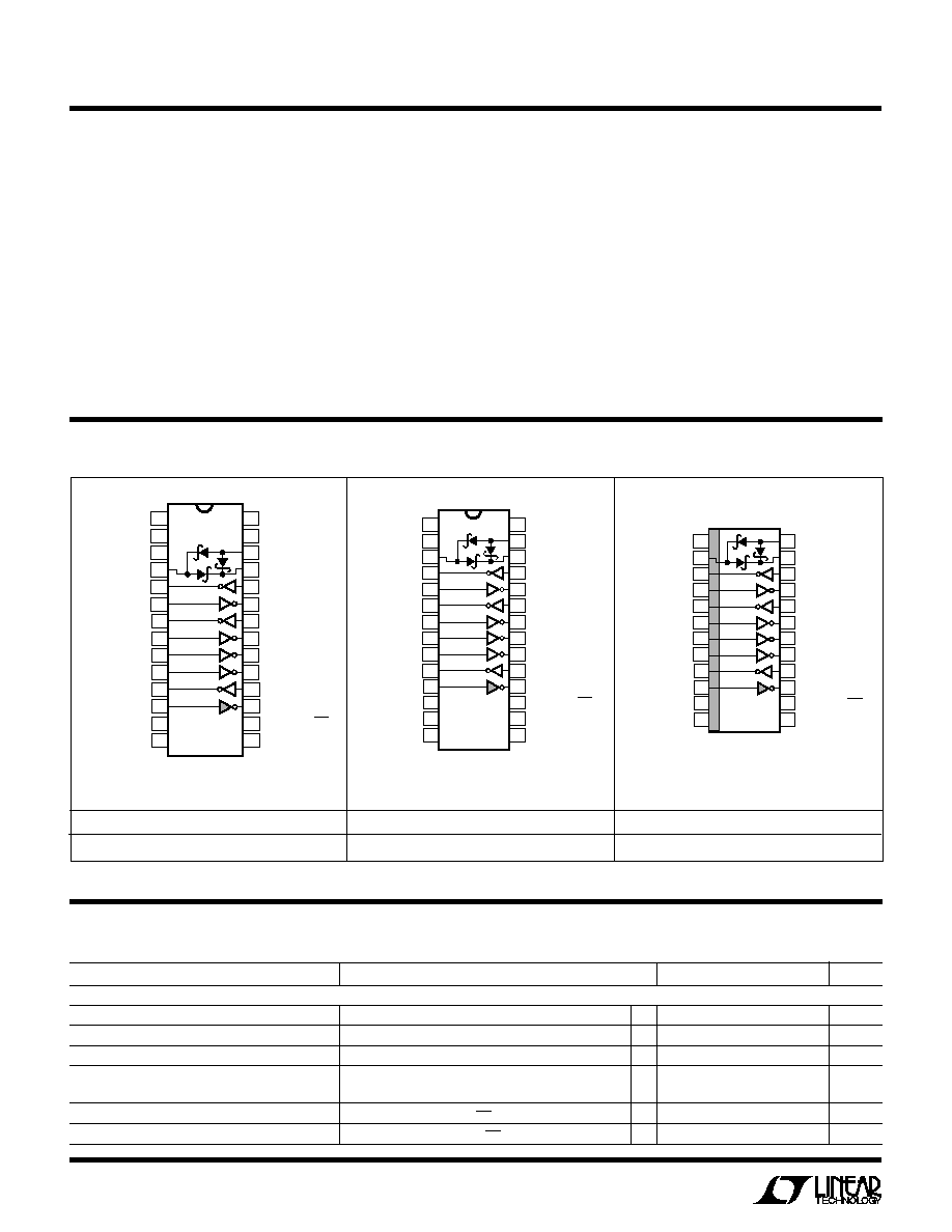
PACKAGE/ORDER I FOR ATIO
ORDER PART NUMBER
1
2
3
4
5
6
7
8
9
10
11
12
13
14
28
27
26
25
24
23
22
21
20
19
18
17
16
15
G PACKAGE
28-LEAD SSOP
TOP VIEW
NC
NC
V
+
C
DRIVER OUT
RX IN
DRIVER OUT
RX IN
RX IN
RX IN
DRIVER OUT
RXA IN
NC
3V V
CC
NC
NC
V
GND
DRIVER IN
RX OUT
DRIVER IN
RX OUT
RX OUT
RX OUT
DRIVER IN
RXA OUT
RS232 ON/OFF
GND
T
JMAX
= 150
°
C,
JA
= 96
°
C/W
ORDER PART NUMBER
ORDER PART NUMBER
(Note 2)
ELECTRICAL C
C
HARA TERISTICS
PARAMETER
CONDITIONS
MIN
TYP
MAX
UNITS
Power Supply
Supply Current I(V
+
)
(Note 3)
0.3
0.8
mA
Supply Current I(V
)
(Note 3)
0.6
1.0
mA
Supply Current I(V
CC
)
(Note 3)
1.0
1.5
mA
Supply Current When OFF I(V
CC
)
(Note 4)
q
0.04
0.10
mA
0.04
0.07
mA
Supply Current When OFF I(V
+
)
V
CC
= 3V, V
+
= 8V, V
ON/OFF
= 0.1V
0.10
0.20
mA
Supply Current When OFF I(V
)
V
CC
= 3V, V
= 8V, V
ON/OFF
= 0.1V
0.10
0.20
mA
1
2
3
4
5
6
7
8
9
10
11
12
13
14
28
27
26
25
24
23
22
21
20
19
18
17
16
15
N PACKAGE
28-LEAD PLASTIC DIP
TOP VIEW
NC
V
+
C
DRIVER OUT
RX IN
DRIVER OUT
RX IN
RX IN
RX IN
DRIVER OUT
RXA IN
NC
3V V
CC
NC
NC
V
GND
DRIVER IN
RX OUT
DRIVER IN
RX OUT
RX OUT
RX OUT
DRIVER IN
RXA OUT
RS232 ON/OFF
GND
NC
T
JMAX
= 150
°
C,
JA
= 56
°
C/W
1
2
3
4
5
6
7
8
9
10
11
12
TOP VIEW
24
23
22
21
20
19
18
17
16
15
14
13
V
+
C
DRIVER OUT
RX IN
DRIVER OUT
RX IN
RX IN
RX IN
DRIVER OUT
RXA IN
NC
3V V
CC
V
GND
DRIVER IN
RX OUT
DRIVER IN
RX OUT
RX OUT
RX OUT
DRIVER IN
RXA OUT
RS232 ON/OFF
GND
S PACKAGE
24-LEAD PLASTIC SOL
T
JMAX
= 150
°
C,
JA
= 80
°
C/W
LT1332CN
LT1332CG
LT1332CS
Consult factory for Industrial and Military grade parts.
3
LT1332
The
q
denotes specifications which apply over the full operating
temperature range.
Note 1: Absolute maximum ratings are those values beyond which the life
of the device may be impaired.
Note 2: Testing is done at V
CC
= 3V, V
+
= 8V, V
= 8V, and
V
ON/OFF
= 3V.
Note 3: Supply current is measured with all driver inputs tied high.
Note 4: Supply current measurements in SHUTDOWN are performed with
V
ON/OFF
= 0.1V, V
+
= 0V, V
= 0V.
ELECTRICAL C
C
HARA TERISTICS
(Note 2)
Note 5: For driver delay measurements, R
L
= 3k and C
L
= 51pF. Trigger
points are set between the driver's input logic threshold and the output
transition to the zero crossing (t
PHL
= 1.4V to 0V and t
PLH
= 1.4V to 0V).
Note 6: Receiver RXA (Pins 10 and 15, S Package) remains functioning in
SHUTDOWN.
Note 7: For receiver delay measurements, C
L
= 51pF. Trigger points are
set between the receiver's input logic threshold and the output transition
to standard TTL/CMOS logic threshold (t
LH
= 1.3V to 2.4V and t
HL
= 1.7V
to 0.8V).
PARAMETER
CONDITIONS
MIN
TYP
MAX
UNITS
Power Supply
ON/OFF Pin Thresholds
Input Low Level (Device Shut Down)
q
0.7
0.3
V
Input High Level (Device Enabled)
q
1.3
0.6
V
ON/OFF Pin Current
0V
V
ON/OFF
5V
q
15
80
µ
A
Drivers
Output Voltage Swing
R
L
= 3k to GND Positive
q
5.0
6.6
V
Negative
q
7.0
5.0
V
Logic Input Voltage Level
Input Low Level (V
OUT
= High)
q
1.4
0.8
V
Input High Level (V
OUT
= Low)
q
2.0
1.4
V
Logic Input Current
0.8V
V
IN
2.0V
q
5
20
µ
A
Output Short-Circuit Current
V
OUT
= 0V
±
17
mA
Output Leakage Current
SHUTDOWN V
OUT
=
±
30V, V
ON/OFF
= 0.1V
q
10
100
µ
A
Driver Output ESD Rating
Human Body Model Discharge
±
10
kV
Slew Rate
R
L
= 3k, C
L
= 51pF
15
30
V/
µ
s
R
L
= 3k, C
L
= 2500pF
4
6
V/
µ
s
Propagation Delay
Output Transition t
PHL
High to Low (Note 5)
0.6
1.3
µ
s
Output Transition t
PLH
Low to High
0.5
1.3
µ
s
Receivers
Input Voltage Thresholds
Input Low Threshold (V
OUT
= High)
0.8
1.3
V
Input High Threshold (V
OUT
= Low)
1.7
2.4
V
Hysteresis
q
0.1
0.4
1.0
V
Input Resistance
3
5
7
k
Receiver Input ESD Rating
Human Body Model Discharge
±
10
kV
Output Voltage
Output Low, I
OUT
= 500
µ
A
q
0.2
0.4
V
Output High, I
OUT
= 100
µ
A (V
CC
= 3V)
q
2.7
2.9
V
Output Leakage Current
SHUTDOWN (Note 6) 0
V
OUT
V
CC
q
1
10
µ
A
Output Short-Circuit Current
Sinking Current, V
OUT
= V
CC
4
2
mA
Sourcing Current, V
OUT
= 0V
2
4
mA
Propagation Delay
Output Transition t
HL
High to Low (Note 7)
1
3
µ
s
Output Transition t
LH
Low to High
0.6
3
µ
s
4
LT1332
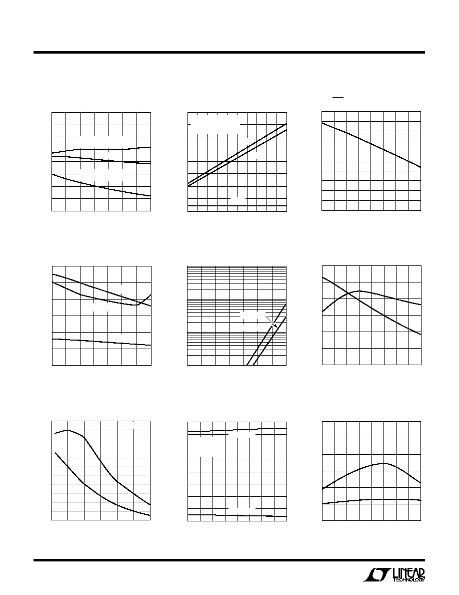
TYPICAL PERFOR A CE CHARACTERISTICS
U
W
TEMPERATURE (°C)
50
SUPPLY CURRENT (mA)
1.4
25
LT1332 · TPC01
0.8
0.4
25
0
50
0.2
0
1.6
1.2
1.0
0.6
75
100
125
I(V
)
DRIVER OUTPUTS HIGH
I(V
+
)
DRIVER OUTPUTS LOW
I(V
CC
)
Unloaded Supply Current
vs Temperature
TEMPERATURE (°C)
50
0
THRESHOLD VOLTAGE (V)
0.1
0.3
0.4
0.5
1.0
0.7
0
50
75
LT1332 · TPC03
0.2
0.8
0.9
0.6
25
25
100 125
150
ON/OFF Threshold vs Temperature
DATA RATE (k BAUD)
0
SUPPLY CURRENT (mA)
12
16
160
LT1332 · TPC02
8
4
0
40
80
120
200
10
14
6
2
140
20
60
100
180
R
L
= 3k
C
L
= 2500pF
ALL DRIVERS LOADED
I(V
)
I(V
+
)
I(V
CC
)
Supply Current vs Data Rate
TEMPERATURE (°C)
50
LEAKAGE CURRENT (
µ
A)
100
125
150
25
75
LT1027 · TPC04
75
50
25
0
50
100
125
25
0
I(V
+
) = 8V
I(V
) = 8V
I(V
CC
) = 3V
TEMPERATURE (°C)
50
10
LEAKAGE CURRENT (
µ
A)
100
0
50
125
LT1332 · TPC05
1
0.1
25
25
75
100
V
OUT
= 30V
V
OUT
= 30V
TEMPERATURE (°C)
50
0
SHORT-CIRCUIT CURRENT (mA)
5
10
15
20
0
50
100
150
LT1332 · TPC06
25
30
25
25
75
125
I
SC
+
I
SC
Driver Output Voltage
vs Temperature
Slew Rate vs Load Capacitance
CAPACITANCE (pF)
0
4
SLEW RATE (V/
µ
s)
6
8
10
12
500
1000
1500
2000
LT1332 · TPC07
2500
3000
14
5
7
9
11
13
15
SR
SR
+
R
L
= 3k
TEMPERATURE (°C)
50
DRIVER OUTPUT VOLTAGE (V)
0
2
4
150
LT1332 · TPC08
2
4
8
0
50
100
6
8
6
25
25
75
125
INPUT LOW
INPUT HIGH
V
+
= 8V
V
= 8V
V
CC
= 3V
Receiver Short-Circuit Current
vs Temperature
TEMPERATURE (°C)
50
0
SHORT-CIRCUIT CURRENT (mA)
5
10
15
20
0
50
100
150
LT1332 · TPC09
25
30
25
25
75
125
I
SC
+
I
SC
Leakage Current in Shutdown
vs Temperature
Driver Leakage in Shutdown
vs Temperature
Driver Short-Circuit Current
vs Temperature
5
LT1332
TYPICAL PERFOR A CE CHARACTERISTICS
U
W
Receiver Input Thresholds
vs Supply Voltage
SUPPLY VOLTAGE (V)
2.0
RECEIVER INPUT THRESHOLD (V)
3
4
5
3.5
4.5
6.0
LT1332 · TPC10
2
1
0
2.5
3.0
4.0
5.0
5.5
V
TH
HIGH
V
TH
LOW
TEMPERATURE (°C)
50
RECEIVER INPUT THRESHOLD (V)
1.5
2.0
2.5
25
75
150
LT1332 · TPC11
1.0
0.5
0
25
0
50
100 125
V
TH
HIGH
V
TH
LOW
V
CC
= 3V
Receiver Input Thresholds
vs Temperature
SUPPLY VOLTAGE (V)
2.0
0
SUPPLY VOLTAGE/RECEIVER OUTPUT (V)
0.1
0.2
0.3
0.4
3.0
4.0
5.0
6.0
LT1332 · TPC12
0.5
0.6
2.5
3.5
4.5
5.5
RECEIVER
OUTPUT LOW
SINKING 500
µ
A
RECEIVER
OUTPUT LOW
SINKING 250
µ
A
RECEIVER
OUTPUT HIGH
(V
CC
V
OUT
)
SOURCING
Receiver Output Voltage
vs Supply Voltage
PI FU CTIO S
U
U
U
V
+
: Positive Supply Input (RS232 Drivers). V
+
should
be greater than 6.5V and less than 13.2V to assure valid
RS232 output signals. An additional decoupling ca-
pacitor may be required if the V
+
generator is located far
away from the LT1332.
V
: Negative Supply Pin (RS232 Drivers). This pin re-
quires an external capacitor. When the device is powered
from a switching regulator, the filter capacitor should be
selected based on the maximum tolerable ripple for the
specified minimum regulator on time. For some low
frequency Burst Mode
TM
regulators, the filter capacitor
should be relatively large (C
10
µ
F). Low ESR tantalum
V
CC
: Input Supply Pin. V
CC
can vary from 2V to 6V to
accommodate a wide range of logic levels, yet the system
still responds correctly to RS232 signals. Supply current
drops to 40
µ
A in the SHUTDOWN mode. This pin should
be decoupled with a 0.1
µ
F ceramic capacitor.
GND: Ground Pins. Pins 13 and 23 (S Package) must both
be grounded for proper operation.
ON/OFF: Controls the operation mode of the device and
is CMOS compatible. A logic low puts the device in the
SHUTDOWN mode which reduces input supply current
to 40
µ
A and places all of the drivers and four of the
receivers in a high impedance state. A logic high fully
enables the device.
Burst Mode
TM
is a trademark of Linear Technology Corporation
Receiver Output Waveforms
LT1332 · TPC13
INPUT
5V/DIV
RX OUTPUT
C
L
= 50pF
2V/DIV
Driver Output Waveforms
LT1332 · TPC13
INPUT
5V/DIV
DRIVER
OUTPUT
R
L
= 3k
C
L
= 2500pF
10V/DIV
DRIVER
OUTPUT
R
L
= 3k
10V/DIV