 | –≠–ª–µ–∫—Ç—Ä–æ–Ω–Ω—ã–π –∫–æ–º–ø–æ–Ω–µ–Ω—Ç: LT1639 | –°–∫–∞—á–∞—Ç—å:  PDF PDF  ZIP ZIP |
1
LT1638/LT1639
1.2MHz, 0.4V/
µ
s
Over-The-Top
TM
Micropower
Rail-to-Rail Input and Output
Op Amps
FEATURES
DESCRIPTIO
N
U
s
Operates with Inputs Above V
+
s
Rail-to-Rail Input and Output
s
Low Power: 230
µ
A per Amplifier Max
s
Gain Bandwidth Product: 1.2MHz
s
Slew Rate: 0.4V/
µ
s
s
High Output Current: 25mA Min
s
Specified on 3V, 5V and
±
15V Supplies
s
Reverse Battery Protection to 18V
s
No Supply Sequencing Problems
s
High Voltage Gain: 1500V/mV
s
Single Supply Input Range: ≠ 0.4V to 44V
s
High CMRR: 98dB
s
No Phase Reversal
APPLICATIO
N
S
U
s
Battery- or Solar-Powered Systems
Portable Instrumentation
Sensor Conditioning
s
Supply Current Sensing
s
Battery Monitoring
s
Micropower Active Filters
s
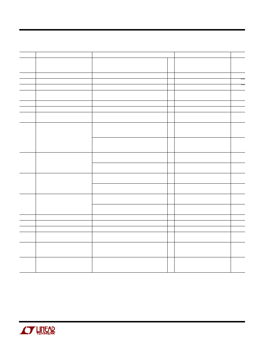
4mA to 20mA Transmitters
V
CC
V
CC
V1
V2
V0
≠
+
A
1/2 LT1638
≠
+
B
1/2 LT1638
V
CC
1M
1M
1M
10k
10k
V
CC
= 5V, V
CM
= 0V TO 44V, t
PD
= 27
µ
s
1638/39 TA01
1M
Over-The-Top Comparator with 100mV Hysteresis Centered at 0mV
TYPICAL APPLICATIO
N
U
Output Voltage vs Input Voltage
5V
0V
The LT
Æ
1638 is a low power dual rail-to-rail input and output
operational amplifier available in the standard 8-pin PDIP and
SO packages as well as the 8-lead MSOP package. The
LT1639 is a low power quad rail-to-rail input and output
operational amplifier offered on the standard 14-pin PDIP
and surface mount packages.
The LT1638/LT1639 op amps operate on all single and
split supplies with a total voltage of 2.5V to 44V drawing
only 170
µ
A of quiescent current per amplifier. These
amplifiers are reverse battery protected and draw no
current for reverse supply up to 18V.
The input range of the LT1638/LT1639 includes both
supplies, and a unique feature of this device is its capability
to operate over the top with either or both of its inputs
above V
+
. The inputs handle 44V, both differential and
common mode, independent of supply voltage. The input
stage incorporates phase reversal protection to prevent
false outputs from occurring even when the inputs are 22V
below the negative supply. Protective resistors are
included in the input leads so that current does not
become excessive when the inputs are forced below the
negative supply. The LT1638/LT1639 can drive loads up to
25mA and still maintain rail-to-rail capability. The op amps
are unity-gain stable and drive all capacitive loads up to
1000pF when optional output compensation is used.
, LTC and LT are registered trademarks of Linear Technology Corporation.
Over-The-Top is a trademark of Linear Technology Corporation.
1638/39 TA02

2
LT1638/LT1639
ABSOLUTE
M
AXI
M
U
M
RATINGS
W
W
W
U
Specified Temperature Range (Note 3) .. ≠ 40
∞
C to 85
∞
C
Junction Temperature ........................................... 150
∞
C
Storage Temperature Range ................. ≠ 65
∞
C to 150
∞
C
Lead Temperature (Soldering, 10 sec) .................. 300
∞
C
Total Supply Voltage (V
+
to V
≠
) .............................. 44V
Input Differential Voltage ......................................... 44V
Input Current ......................................................
±
25mA
Output Short-Circuit Duration (Note 2) ......... Continuous
Operating Temperature Range ................ ≠ 40
∞
C to 85
∞
C
PACKAGE/ORDER I
N
FOR
M
ATIO
N
W
U
U
ORDER PART NUMBER
ORDER PART NUMBER
LT1638CMS8
LT1638CS8
LT1638IS8
LT1638CN8
LT1638IN8
MS8 PART MARKING
S8 PART MARKING
1638I
1638
TOP VIEW
S PACKAGE
14-LEAD PLASTIC SO
N PACKAGE
14-LEAD PDIP
1
2
3
4
5
6
7
14
13
12
11
10
9
8
A
B
C
OUT A
≠IN A
+IN A
V
+
+IN B
≠IN B
OUT B
OUT D
≠IN D
+IN D
V
≠
+IN C
≠ IN C
OUT C
D
ORDER PART NUMBER
LT1639CS
LT1639IS
LT1639CN
LT1639IN
T
JMAX
= 150
∞
C,
JA
= 110
∞
C/ W (N)
T
JMAX
= 150
∞
C,
JA
= 150
∞
C/ W (S)
1
2
3
4
OUT A
≠IN A
+IN A
V
≠
8
7
6
5
V+
OUT B
≠IN B
+IN B
TOP VIEW
MS8 PACKAGE
8-LEAD PLASTIC MSOP
T
JMAX
= 150
∞
C,
JA
= 250
∞
C/ W (MS8)
1
2
3
4
8
7
6
5
TOP VIEW
N8 PACKAGE
8-LEAD PDIP
S8 PACKAGE
8-LEAD PLASTIC SO
V
+
OUT B
≠IN B
+IN B
A
B
OUT A
≠IN A
+IN A
V
≠
T
JMAX
= 150
∞
C,
JA
= 130
∞
C/ W (N8)
T
JMAX
= 150
∞
C,
JA
= 190
∞
C/ W (S8)
LTCY
SYMBOL
PARAMETER
CONDITIONS
MIN
TYP
MAX
UNITS
V
OS
Input Offset Voltage
LT1638 N, S Packages
200
600
µ
V
0
∞
C
T
A
70
∞
C
q
850
µ
V
≠ 40
∞
C
T
A
85
∞
C
q
950
µ
V
LT1639 N, S Packages
300
700
µ
V
0
∞
C
T
A
70
∞
C
q
950
µ
V
≠ 40
∞
C
T
A
85
∞
C
q
1050
µ
V
LT1638C MS8 Package
350
900
µ
V
0
∞
C
T
A
70
∞
C
q
1150
µ
V
≠ 40
∞
C
T
A
85
∞
C
q
1250
µ
V
Input Offset Voltage Drift
LT1638/LT1639 N, S Packages
q
2
6
µ
V/
∞
C
(Note 7)
LT1638CMS8
q
2.5
7
µ
V/
∞
C
I
OS
Input Offset Current
q
1
6
nA
V
CM
= 44V (Note 4)
q
2.5
µ
A
V
S
= 3V, 0V; V
S
= 5V, 0V; V
CM
= V
OUT
= half supply, T
A
= 25
∞
C, unless otherwise noted. (Note 3)
Consult factory for Military grade parts.
ELECTRICAL CHARACTERISTICS
(Note 1)
3
LT1638/LT1639
ELECTRICAL CHARACTERISTICS
SYMBOL
PARAMETER
CONDITIONS
MIN
TYP
MAX
UNITS
I
B
Input Bias Current
q
20
50
nA
V
CM
= 44V (Note 4)
q
8
30
µ
A
V
S
= 0V
0.1
nA
Input Noise Voltage
0.1Hz to 10Hz
1
µ
V
P-P
e
n
Input Noise Voltage Density
f = 1kHz
20
nV/
Hz
i
n
Input Noise Current Density
f = 1kHz
0.3
pA/
Hz
R
IN
Input Resistance
Differential
1
2.5
M
Common Mode, V
CM
= 0V to 44V
1.4
5.5
M
C
IN
Input Capacitance
5
pF
Input Voltage Range
q
0
44
V
CMRR
Common Mode Rejection Ratio
V
CM
= 0V to V
CC
≠ 1V
q
88
98
dB
V
CM
= 0V to 44V (Note 8)
q
80
88
dB
A
VOL
Large-Signal Voltage Gain
V
S
= 3V, V
O
= 500mV to 2.5V, R
L
= 10k
200
1500
V/mV
0
∞
C
T
A
70
∞
C
q
133
V/mV
≠ 40
∞
C
T
A
85
∞
C
q
100
V/mV
V
S
= 5V, V
O
= 500mV to 4.5V, R
L
= 10k
400
1500
V/mV
0
∞
C
T
A
70
∞
C
q
250
V/mV
≠ 40
∞
C
T
A
85
∞
C
q
200
V/mV
V
OL
Output Voltage Swing Low
V
S
= 3V, No Load
q
3
8
mV
V
S
= 3V, I
SINK
= 5mA
q
250
450
mV
V
S
= 5V, No Load
q
3
8
mV
V
S
= 5V, I
SINK
= 10mA
q
500
700
mV
V
OH
Output Voltage Swing High
V
S
= 3V, No Load
q
2.94
2.98
V
V
S
= 3V, I
SOURCE
= 5mA
q
2.25
2.40
V
V
S
= 5V, No Load
q
4.94
4.98
V
V
S
= 5V, I
SOURCE
= 10mA
q
3.8
4.0
V
I
SC
Short-Circuit Current (Note 2)
V
S
= 3V, Short to GND
10
15
mA
V
S
= 3V, Short to V
CC
15
25
mA
V
S
= 5V, Short to GND
15
20
mA
V
S
= 5V, Short to V
CC
15
25
mA
PSRR
Power Supply Rejection Ratio
V
S
= 3V to 12.5V, V
CM
= V
O
= 1V
q
90
100
dB
Reverse Supply Voltage
I
S
= ≠ 100
µ
A per Amplifier
q
18
27
V
Minimum Operating Supply Voltage
q
2.4
2.7
V
I
S
Supply Current per Amplifier
170
230
µ
A
(Note 5)
q
275
µ
A
GBW
Gain Bandwidth Product
f = 1kHz
650
1075
kHz
(Note 4)
0
∞
C
T
A
70
∞
C
q
550
kHz
≠ 40
∞
C
T
A
85
∞
C
q
500
kHz
SR
Slew Rate
A
V
= ≠ 1, R
L
=
0.210
0.38
V/
µ
s
(Note 6)
0
∞
C
T
A
70
∞
C
q
0.185
V/
µ
s
≠ 40
∞
C
T
A
85
∞
C
q
0.170
V/
µ
s
V
S
= 3V, 0V; V
S
= 5V, 0V; V
CM
= V
OUT
= half supply, T
A
= 25
∞
C, unless otherwise noted. (Note 3)
4
LT1638/LT1639
ELECTRICAL CHARACTERISTICS
V
S
=
±
15V, V
CM
= 0V, V
OUT
= 0V, T
A
= 25
∞
C, unless otherwise noted. (Note 3)
SYMBOL
PARAMETER
CONDITIONS
MIN
TYP
MAX
UNITS
V
OS
Input Offset Voltage
LT1638 N, S Packages
250
800
µ
V
0
∞
C
T
A
70
∞
C
q
1000
µ
V
≠ 40
∞
C
T
A
85
∞
C
q
1100
µ
V
LT1639 N, S Packages
350
900
µ
V
0
∞
C
T
A
70
∞
C
q
1100
µ
V
≠ 40
∞
C
T
A
85
∞
C
q
1200
µ
V
LT1638C MS8 Package
400
1050
µ
V
0
∞
C
T
A
70
∞
C
q
1250
µ
V
≠ 40
∞
C
T
A
85
∞
C
q
1350
µ
V
Input Offset Voltage Drift
LT1638/LT1639 N, S Packages
q
2
6
µ
V/
∞
C
(Note 7)
LT1638CMS8
q
2.5
7
µ
V/
∞
C
I
OS
Input Offset Current
q
1
6
nA
I
B
Input Bias Current
q
20
50
nA
Input Noise Voltage
0.1Hz to 10Hz
1
µ
V
P-P
e
n
Input Noise Voltage Density
f = 1kHz
20
nV/
Hz
i
n
Input Noise Current Density
f = 1kHz
0.3
pA/
Hz
R
IN
Input Resistance
Differential
1
2.5
M
Common Mode, V
CM
= ≠ 15V to 14V
500
M
C
IN
Input Capacitance
4.5
pF
Input Voltage Range
q
≠ 15
29
V
CMRR
Common Mode Rejection Ratio
V
CM
= ≠15V to 29V
q
80
88
dB
A
VOL
Large-Signal Voltage Gain
V
O
=
±
14V, R
L
= 10k
200
500
V/mV
0
∞
C
T
A
70
∞
C
q
125
V/mV
≠ 40
∞
C
T
A
85
∞
C
q
100
V/mV
V
OL
Output Voltage Swing
No Load
q
14.9
14.95
V
I
OUT
=
±
10mA
q
13.7
14.0
V
I
SC
Short-Circuit Current (Note 2)
Short to GND
25
40
mA
0
∞
C
T
A
70
∞
C
q
20
mA
≠ 40
∞
C
T
A
85
∞
C
q
15
mA
PSRR
Power Supply Rejection Ratio
V
S
=
±
1.5V to
±
22V
q
90
100
dB
I
S
Supply Current per Amplifier
205
280
µ
A
q
350
µ
A
GBW
Gain Bandwidth Product
f = 1kHz
750
1200
kHz
0
∞
C
T
A
70
∞
C
q
650
kHz
≠ 40
∞
C
T
A
85
∞
C
q
600
kHz
SR
Slew Rate
A
V
= ≠ 1, R
L
=
,
V
O
=
±
10V,
0.225
0.4
V/
µ
s
0
∞
C
T
A
70
∞
C
q
0.2
V/
µ
s
≠ 40
∞
C
T
A
85
∞
C
q
0.18
V/
µ
s
The
q
denotes specifications which apply over the full specified
temperature range.
Note 1: Absolute Maximum Ratings are those values beyond which the
life of a device may be impaired.
Note 2: A heat sink may be required to keep the junction temperature
below absolute maximum. This depends on the power supply voltage
and how many amplifiers are shorted.
Note 3: The LT1638C/LT1639C are guaranteed to meet 0
∞
C to 70
∞
C
specifications and are designed, characterized and expected to meet
the extended temperature limits, but are not tested at ≠ 40
∞
C and 85
∞
C.
The LT1638I/LT1639I are guaranteed to meet the extended
temperature limits.
Note 4: V
S
= 5V limits are guaranteed by correlation to V
S
= 3V and
V
S
=
±
15V tests.
Note 5: V
S
= 3V limits are guaranteed by correlation to V
S
= 5V and
V
S
=
±
15V tests.
Note 6: Guaranteed by correlation to slew rate at V
S
=
±
15V and GBW
at V
S
= 3V and V
S
=
±
15V tests.
Note 7: This parameter is not 100% tested.
Note 8: The spec implies a typical offset voltage at V
CM
= 44 of 2mV and
a maximum offset voltage at V
CM
= 44 of 5mV.

5
LT1638/LT1639
TYPICAL PERFOR
M
A
N
CE CHARACTERISTICS
U
W
Minimum Supply Voltage
Input Bias Current vs
Common Mode Voltage
Output Saturation Voltage vs
Load Current (Output High)
0.1Hz to 10Hz Noise Voltage
Noise Voltage Density vs
Frequency
SUPPLY VOLTAGE (V)
0
SUPPLY CURRENT PER AMPLIFIER (
µ
A)
10
20
25
45
1638/39 G01
300
280
260
240
220
200
180
160
140
120
100
5
15
30
35
40
T
A
= 125
∞
C
T
A
= 25
∞
C
T
A
= ≠55
∞
C
Supply Current vs Supply Voltage
TOTAL SUPPLY VOLTAGE (V)
0
CHANGE IN INPUT OFFSET VOLTAGE (
µ
V)
200
400
4
1638/39 G02
0
≠200
100
300
≠100
≠300
≠ 400
1
2
3
5
T
A
=
125
∞
C
T
A
=
≠55
∞
C
T
A
=
25
∞
C
COMMON MODE VOLTAGE (V)
4.0
INPUT BIAS CURRENT (nA)
10000
8000
6000
60
40
20
0
≠20
≠40
5.6
1638/39 G03
4.4
4.8
5.2
44
T
A
=
125
∞
C
T
A
=
≠55
∞
C
T
A
=
25
∞
C
V
S
= 5V, 0V
FREQUENCY (Hz)
1
INPUT NOISE VOLTAGE DENSITY (nV/
Hz)
10
100
1k
1638/39 G09
70
60
50
40
30
20
10
0
TIME (SEC)
0
1
3
5
7
9
NOISE VOLTAGE (400nV/DIV)
2
4
6
8
1638/39 G07
10
V
S
=
±
2.5
FREQUENCY (Hz)
1
4.5
4.0
3.5
3.0
2.5
2.0
1.5
1.0
0.5
0
10
100
1k
1638/39 G08
INPUT NOISE CURRENT DENSITY (pA/
Hz)
SOURCING LOAD CURRENT (mA)
0.001
0.01
OUTPUT SATURATION VOLTAGE (V)
0.1
1
0.01
0.1
1
10
1638/39 G04
V
S
=
±
2.5V
V
OD
= 30mV
T
A
= 125
∞
C
T
A
= ≠55
∞
C
T
A
= 25
∞
C
SINKING LOAD CURRENT (mA)
0.001
0.001
OUTPUT SATURATION VOLTAGE (V)
0.1
0.01
1
0.01
0.1
1
10
1638/39 G05
V
S
=
±
2.5V
V
OD
= 30mV
T
A
= 125
∞
C
T
A
= ≠55
∞
C
T
A
= 25
∞
C
INPUT OVERDRIVE (mV)
10
OUTPUT SATURATION VOLTAGE (mV)
30
100
1638/39 G06
1
10
20
100
90
80
70
60
50
40
0
V
S
=
±
2.5V
NO LOAD
OUTPUT HIGH
OUTPUT LOW
Output Saturation Voltage vs
Input Overdrive
Output Saturation Voltage vs
Load Current (Output Low)
Input Noise Current Density
vs Frequency