 | ÐлекÑÑоннÑй компоненÑ: LT1714 | СкаÑаÑÑ:  PDF PDF  ZIP ZIP |
171314f.pm6
1
LT1713/LT1714
Single/Dual, 7ns, Low Power,
3V/5V/
±
5V Rail-to-Rail Comparators
The LT
®
1713/LT1714 are UltraFast
TM
7ns, single/dual
comparators featuring rail-to-rail inputs, rail-to-rail
complementary outputs and an output latch. Optimized
for 3V and 5V power supplies, they operate over a single
supply voltage range from 2.4V to 12V or from
±
2.4V to
±
6V dual supplies.
The LT1713/LT1714 are designed for ease of use in a
variety of systems. In addition to wide supply voltage
flexibility, rail-to-rail input common mode range extends
100mV beyond both supply rails and the outputs are
protected against phase reversal for inputs extending
further beyond the rails. Also, the rail-to-rail inputs may be
taken to opposite rails with no significant increase in input
current. The rail-to-rail matched complementary outputs
interface directly to TTL or CMOS logic and can sink 10mA
to within 0.5V of GND or source 10mA to within 0.7V of V
+
.
The LT1713/LT1714 have internal TTL/CMOS compatible
latches for retaining data at the outputs. Each latch holds
data as long as its latch pin is held high. Latch pin
hysteresis provides protection against slow moving or
noisy latch signals. The LT1713 is available in the 8-lead
MSOP package. The LT1714 is available in the 16-lead
narrow SSOP package.
s
Ultrafast: 7ns at 20mV Overdrive
8.5ns at 5mV Overdrive
s
Rail-to-Rail Inputs
s
Rail-to-Rail Complementary Outputs
(TTL/CMOS Compatible)
s
Specified at 2.7V, 5V and
±
5V Supplies
s
Low Power (Per Comparator): 5mA
s
Output Latch
s
Inputs Can Exceed Supplies Without Phase Reversal
s
LT1713: 8-Lead MSOP Package
s
LT1714: 16-Lead Narrow SSOP Package
, LTC and LT are registered trademarks of Linear Technology Corporation.
s
High Speed Automatic Test Equipment
s
Current Sense for Switching Regulators
s
Crystal Oscillator Circuits
s
High Speed Sampling Circuits
s
High Speed A/D Converters
s
Pulse Width Modulators
s
Window Comparators
s
Extended Range V/F Converters
s
Fast Pulse Height/Width Discriminators
s
Line Receivers
s
High Speed Triggers
UltraFast is a trademark of Linear Technology Corporation.
LT1713/LT1714 Propagation Delay
vs Input Overdrive
FEATURES
DESCRIPTIO
U
APPLICATIO S
U
TYPICAL APPLICATIO
U
A 4
×
NTSC Subcarrier Voltage-Tunable Crystal Oscillator
171314 TA01
+
LT1713
5V
390
200pF
* 1% FILM RESISTOR
** NORTHERN ENGINEERING LABS C-2350N-14.31818MHz
5V
FREQUENCY
OUTPUT
3.9k*
V
IN
0V TO 5V
1M
MV-209
VARACTOR
DIODE
2k
2k
100pF
15pF
Y1**
100pF
0.047
µ
F
C SELECT
(CHOOSE FOR CORRECT
PLL LOOP RESPONSE)
1M
1M
1M*
1N4148
LT1004-2.5
47k*
1k*
INPUT OVERDRIVE (mV)
0
PROPAGATION DELAY (ns)
6.5
7.0
7.5
t
PD
+
t
PD
30
50
171314 TA02
6.0
5.5
5.0
10
20
40
8.0
8.5
9.0
60
T
A
= 25
°
C
V
+
= 5V
V
= 0V
V
STEP
= 100mV
2
LT1713/LT1714
Supply Voltage
V
+
to V
............................................................ 12.6V
V
+
to GND ........................................................ 12.6V
V
to GND ............................................. 10V to 0.3V
Differential Input Voltage ...................................
±
12.6V
Latch Pin Voltage ...................................................... 7V
Input and Latch Current .....................................
±
10mA
ORDER PART
NUMBER
LT1714CGN
LT1714IGN
T
JMAX
= 150
°
C,
JA
= 120
°
C/ W
PACKAGE/ORDER I FOR ATIO
U
U
W
GN PART MARKING
1714
1714I
ABSOLUTE AXI U RATI GS
W
W
W
U
(Note 1)
Output Current (Continuous) ..............................
±
20mA
Operating Temperature Range ................ 40
°
C to 85
°
C
Specified Temperature Range (Note 2) ... 40
°
C to 85
°
C
Junction Temperature .......................................... 150
°
C
Storage Temperature Range ................. 65
°
C to 150
°
C
Lead Temperature (Soldering, 10 sec).................. 300
°
C
ORDER PART
NUMBER
LT1713CMS8
LT1713IMS8
MS8 PART MARKING
LTRD
LTUK
Consult factory for parts specified with wider operating temperature ranges.
T
JMAX
= 150
°
C,
JA
= 250
°
C/ W
1
2
3
4
V
+
+IN
IN
V
8
7
6
5
Q OUT
Q OUT
GND
LATCH
ENABLE
TOP VIEW
MS8 PACKAGE
8-LEAD PLASTIC MSOP
GN PACKAGE
16-LEAD PLASTIC SSOP
1
2
3
4
5
6
7
8
TOP VIEW
16
15
14
13
12
11
10
9
IN A
+IN A
V
V
+
V
+
V
+IN B
IN B
GND
Q A
Q A
Q B
Q B
GND
LATCH
ENABLE B
LATCH
ENABLE A
SYMBOL
PARAMETER
CONDITIONS
MIN
TYP
MAX
UNITS
V
+
Positive Supply Voltage Range
q
2.4
7
V
V
OS
Input Offset Voltage (Note 4)
R
S
= 50
, V
CM
= V
+
/2
0.5
4
mV
R
S
= 50
, V
CM
= V
+
/2 (Note 11)
q
5
mV
R
S
= 50
, V
CM
= 0V
0.7
mV
R
S
= 50
, V
CM
= V
+
1
mV
V
OS
/
T
Input Offset Voltage Drift
q
5
µ
V/
°
C
I
OS
Input Offset Current
0.1
1
µ
A
q
2
µ
A
I
B
Input Bias Current (Note 5)
7
1.5
2
µ
A
q
15
5
µ
A
V
CM
Input Voltage Range (Note 9)
q
0.1
V
+
+ 0.1
V
CMRR
Common Mode Rejection Ratio
V
+
= 5V, 0V
V
CM
5V
60
70
dB
V
+
= 5V, 0V
V
CM
5V
q
58
dB
V
+
= 2.7V, 0V
V
CM
2.7V
57
70
dB
V
+
= 2.7V, 0V
V
CM
2.7V
q
55
dB
The
q
denotes specifications which apply over the full operating temperature range, otherwise specifications are at T
A
= 25
°
C.
V
+
= 2.7V or V
+
= 5V, V
= 0V, V
CM
= V
+
/2, V
LATCH
= 0.8V, C
LOAD
= 10pF, V
OVERDRIVE
= 20mV, unless otherwise specified.
ELECTRICAL CHARACTERISTICS
3
LT1713/LT1714
SYMBOL
PARAMETER
CONDITIONS
MIN
TYP
MAX
UNITS
PSRR
+
Positive Power Supply Rejection Ratio
2.4V
V
+
7V, V
CM
= 0V
65
80
dB
q
60
dB
PSRR
Negative Power Supply Rejection Ratio
7V
V
0V, V
+
= 5V, V
CM
= 5V
65
80
dB
q
60
dB
A
V
Small-Signal Voltage Gain (Note 10)
1.5
3
V/mV
V
OH
Output Voltage Swing HIGH
I
OUT
= 1mA, V
+
= 5V, V
OVERDRIVE
= 50mV
q
V
+
0.5 V
+
0.2
V
I
OUT
= 10mA, V
+
= 5V, V
OVERDRIVE
= 50mV
q
V
+
0.7 V
+
0.4
V
V
OL
Output Voltage Swing LOW
I
OUT
= 1mA, V
OVERDRIVE
= 50mV
q
0.20
0.4
V
I
OUT
= 10mA, V
OVERDRIVE
= 50mV
q
0.35
0.5
V
I
+
Positive Supply Current (Per Comparator)
V
+
= 5V, V
OVERDRIVE
= 1V
5
6.5
mA
q
8.0
mA
I
Negative Supply Current (Per Comparator)
V
+
= 5V, V
OVERDRIVE
= 1V
3
4.0
mA
q
4.5
mA
V
IH
Latch Pin High Input Voltage
q
2.4
V
V
IL
Latch Pin Low Input Voltage
q
0.8
V
I
IL
Latch Pin Current
V
LATCH
= V
+
q
10
µ
A
t
PD
Propagation Delay (Note 6)
V
IN
= 100mV, V
OVERDRIVE
= 20mV
8.0
11.0
ns
V
IN
= 100mV, V
OVERDRIVE
= 20mV
q
12.5
ns
V
IN
= 100mV, V
OVERDRIVE
= 5mV
9.0
ns
t
PD
Differential Propagation Delay (Note 6)
V
IN
= 100mV, V
OVERDRIVE
= 20mV
0.5
3
ns
t
r
Output Rise Time
10% to 90%
4
ns
t
f
Output Fall Time
90% to 10%
4
ns
t
LPD
Latch Propagation Delay (Note 7)
8
ns
t
SU
Latch Setup Time (Note 7)
1.5
ns
t
H
Latch Hold Time (Note 7)
0
ns
t
DPW
Minimum Latch Disable Pulse Width (Note 7)
8
ns
f
MAX
Maximum Toggle Frequency
V
IN
= 100mV
P-P
Sine Wave
65
MHz
t
JITTER
Output Timing Jitter
V
IN
= 630mV
P-P
(0dBm) Sine Wave, f = 30MHz
15
ps
RMS
The
q
denotes specifications which apply over the full operating temperature range, otherwise specifications are at T
A
= 25
°
C.
V
+
= 2.7V or V
+
= 5V, V
= 0V, V
CM
= V
+
/2, V
LATCH
= 0.8V, C
LOAD
= 10pF, V
OVERDRIVE
= 20mV, unless otherwise specified.
ELECTRICAL CHARACTERISTICS
The
q
denotes specifications which apply over the full operating temperature range, otherwise specifications are at T
A
= 25
°
C.
V
+
= 5V, V
= 5V, V
CM
= 0V, V
LATCH
= 0.8V, C
LOAD
= 10pF, V
OVERDRIVE
= 20mV, unless otherwise specified.
SYMBOL
PARAMETER
CONDITIONS
MIN
TYP
MAX
UNITS
V
+
Positive Supply Voltage Range
q
2.4
7
V
V
Negative Supply Voltage Range (Note 3)
q
7
0
V
V
OS
Input Offset Voltage (Note 4)
R
S
= 50
, V
CM
= 0V
0.5
3
mV
R
S
= 50
, V
CM
= 0V
q
4
mV
R
S
= 50
, V
CM
= 5V
0.7
mV
R
S
= 50
, V
CM
= 5V
1
mV
V
OS
/
T
Input Offset Voltage Drift
q
5
µ
V/
°
C
I
OS
Input Offset Current
0.1
1
µ
A
q
2
µ
A
I
B
Input Bias Current (Note 5)
7
1.5
2
µ
A
q
15
5
µ
A
4
LT1713/LT1714
ELECTRICAL CHARACTERISTICS
SYMBOL
PARAMETER
CONDITIONS
MIN
TYP
MAX
UNITS
V
CM
Input Voltage Range
q
5.1
5.1
V
CMRR
Common Mode Rejection Ratio
5V
V
CM
5V
62
70
dB
q
60
dB
PSRR
+
Positive Power Supply Rejection Ratio
2.4V
V
+
7V, V
CM
= 5V
68
80
dB
q
65
dB
PSRR
Negative Power Supply Rejection Ratio
7V
V
0V, V
CM
= 5V
65
80
dB
q
60
dB
A
V
Small-Signal Voltage Gain (Note 10)
1V
V
OUT
4V, R
L
=
1.5
3
V/mV
V
OH
Output Voltage Swing HIGH (Note 8)
I
OUT
= 1mA, V
OVERDRIVE
= 50mV
q
4.5
4.8
V
I
OUT
= 10mA, V
OVERDRIVE
= 50mV
q
4.3
4.6
V
V
OL
Output Voltage Swing LOW (Note 8)
I
OUT
= 1mA, V
OVERDRIVE
= 50mV
q
0.20
0.4
V
I
OUT
= 10mA, V
OVERDRIVE
= 50mV
q
0.35
0.5
V
I
+
Positive Supply Current (Per Comparator)
V
OVERDRIVE
= 1V
5.5
7.5
mA
q
9.0
mA
I
Negative Supply Current (Per Comparator)
V
OVERDRIVE
= 1V
3.5
4.5
mA
q
5.0
mA
V
IH
Latch Pin High Input Voltage
q
2.4
V
V
IL
Latch Pin Low Input Voltage
q
0.8
V
I
IL
Latch Pin Current
V
LATCH
= V
+
q
10
µ
A
t
PD
Propagation Delay (Note 6)
V
IN
= 100mV, V
OVERDRIVE
= 20mV
7
10
ns
V
IN
= 100mV, V
OVERDRIVE
= 20mV
q
12
ns
V
IN
= 100mV, V
OVERDRIVE
= 5mV
8.5
ns
t
PD
Differential Propagation Delay (Note 6)
V
IN
= 100mV, V
OVERDRIVE
= 20mV
0.5
3
ns
t
r
Output Rise Time
10% to 90%
4
ns
t
f
Output Fall Time
90% to 10%
4
ns
t
LPD
Latch Propagation Delay (Note 7)
8
ns
t
SU
Latch Setup Time (Note 7)
1.5
ns
t
H
Latch Hold Time (Note 7)
0
ns
t
DPW
Minimum Latch Disable Pulse Width (Note 7)
8
ns
f
MAX
Maximum Toggle Frequency
V
IN
= 100mV
P-P
Sine Wave
65
MHz
t
JITTER
Output Timing Jitter
V
IN
= 630mV
P-P
(0dBm) Sine Wave, f = 30MHz
15
ps
RMS
The
q
denotes specifications which apply over the full operating temperature range, otherwise specifications are at T
A
= 25
°
C.
V
+
= 5V, V
= 5V, V
CM
= 0V, V
LATCH
= 0.8V, C
LOAD
= 10pF, V
OVERDRIVE
= 20mV, unless otherwise specified.
Note 1: Absolute Maximum Ratings are those values beyond which the life
of a device may be impaired.
Note 2: The LT1713C/LT1714C are guaranteed to meet specified
performance from 0
°
C to 70
°
C. They are designed, characterized and
expected to meet specified performance from 40
°
C to 85
°
C but are not
tested or QA sampled at these temperatures. The LT1713I/LT1714I are
guaranteed to meet specified performance from 40
°
C to 85
°
C.
Note 3: The negative supply should not be greater than the ground pin
voltages and the maximum voltage across the positive and negative
supplies should not be greater than 12V.
Note 4: Input offset voltage (V
OS
) is defined as the average of the two
voltages measured by forcing first one output, then the other to V
+
/2.
Note 5: Input bias current (I
B
) is defined as the average of the two input
currents.
Note 6: Propagation delay (t
PD
) is measured with the overdrive added to
the actual V
OS
. Differential propagation delay is defined as:
t
PD
= t
PD
+
t
PD
. Load capacitance is 10pF. Due to test system
requirements, the LT1713/LT1714 propagation delay is specified with a
1k
load to ground for
±
5V supplies, or to mid-supply for 2.7V or 5V
single supplies.
Note 7: Latch propagation delay (t
LPD
) is the delay time for the output to
respond when the latch pin is deasserted. Latch setup time (t
SU
) is the
interval in which the input signal must remain stable prior to asserting the
latch signal. Latch hold time (t
H
) is the interval after the latch is asserted in
which the input signal must remain stable. Latch disable pulse width
(t
DPW
) is the width of the negative pulse on the latch enable pin that
latches in new data on the data inputs.
5
LT1713/LT1714
Note 8: Output voltage swings are characterized and tested at V
+
= 5V and
V
= 0V. They are designed and expected to meet these same
specifications at V
= 5V.
Note 9: The input voltage range is tested under the more demanding
conditions of V
+
= 5V and V
= 5V. The LT1713/LT1714 are designed
and expected to meet these specifications at V
= 0V.
ELECTRICAL CHARACTERISTICS
Note 10: The LT1713/LT1714 voltage gain is tested at V
+
= 5V and
V
= 5V only. Voltage gain at single supply V
+
= 5V and V
+
= 2.7V is
guaranteed by design and correlation.
Note 11: Input offset voltage over temperature at V
+
= 2.7V is guaranteed
by design and characterization.
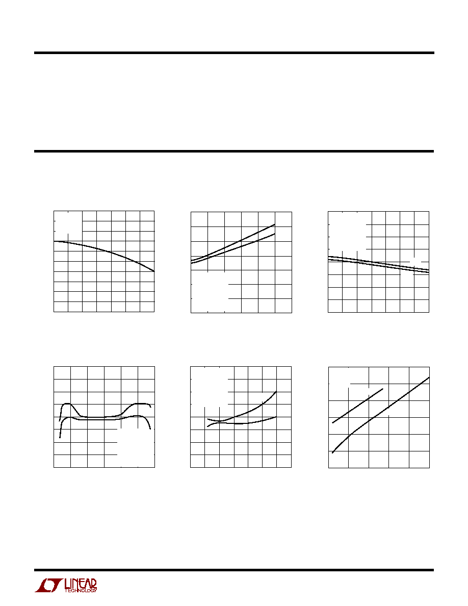
TYPICAL PERFOR A CE CHARACTERISTICS
U
W
Propagation Delay
vs Load Capacitance
Input Offset Voltage
vs Temperature
TEMPERATURE (
°
C)
50
INPUT OFFSET VOLTAGE (mV)
2.5
2.0
1.5
1.0
0.5
0
0.5
1.0
1.5
2.0
2.5
0
50
75
171314 G01
25
25
100
125
V
+
= 5V
V
= 0V
V
CM
= 2.5V
LOAD CAPACITANCE (pF)
0
60
100
171314 G02
20
14
12
10
8
t
PD
+
6
4
2
0
40
80
120
PROPAGATION DELAY (ns)
t
PD
T
A
= 25
°
C
V
+
= 5V
V
= 0V
V
CM
= 2.5V
V
OD
= 20mV
V
STEP
= 100mV
TEMPERATURE (
°
C)
50
PROPAGATION DELAY (ns)
100
171314 G03
0
50
16
14
12
10
8
6
4
2
0
25
25
75
125
t
PD
+
t
PD
V
+
= 5V
V
= 0V
V
CM
= 2.5V
V
OD
= 20mV
V
STEP
= 100mV
C
LOAD
= 10pF
Propagation Delay
vs Input Common Mode Voltage
Propagation Delay
vs Positive Supply Voltage
Positive Supply Current
vs Positive Supply Voltage
Propagation Delay
vs Temperature
INPUT COMMON MODE (V)
0.5
PROPAGATION DELAY (ns)
7.5
8.0
t
PD
+
t
PD
8.5
2.5
4.5
171314 G04
7.0
6.5
6.0
0.5
1.5
3.5
9.0
9.5
10.0
5.5
T
A
= 25
°
C
V
+
= 5V
V
= 0V
V
OD
= 20mV
V
STEP
= 100mV
C
LOAD
= 10pF
POSITIVE SUPPLY VOLTAGE (V)
0
PROPAGATION DELAY (ns)
9.5
6
171314 G05
8.0
7.0
2
4
8
6.5
6.0
10.0
9.0
8.5
7.5
10
12
14
t
PD
T
A
= 25
°
C
V
= 0V
V
CM
= 2.5V
V
OD
= 20mV
V
STEP
= 100mV
C
LOAD
= 10pF
t
PD
+
POSITIVE SUPPLY VOLTAGE (V)
2
4.0
POSITIVE SUPPLY CURRENT (PER COMPARATOR) (mA)
4.5
5.0
5.5
6.0
7.0
4
6
8
10
171314 G06
12
6.5
V
= 5V
V
= 0V
T
A
= 25
°
C
V
IN
= 100mV
I
OUT
= 0