 | ÐлекÑÑоннÑй компоненÑ: LT1796 | СкаÑаÑÑ:  PDF PDF  ZIP ZIP |
1796i.pm6
1
LT1796
1796f
FEATURES
DESCRIPTIO
U
APPLICATIO S
U
TYPICAL APPLICATIO
U
Overvoltage Fault Protected
CAN Transceiver
s
Protected from Overvoltage Line Faults to
±
60V
s
ESD Protection to IEC-1000-4-2 Level 4
±
15kV Air Gap Test
±
8kV Contact Mode Test
s
ISO 11898 Compatible
s
High Input Impedance Supports Up to 256 Nodes
s
Controlled Slew Rates for EMI Emissions Control
s
High Impedance Outputs When Off or
Powered Down
s
Short-Circuit Protection On All Outputs
s
Thermal Shutdown Protection
s
Pin Compatible with Philips PCA82C251
s
Industrial Control Data Networks
s
Automotive Systems
s
HVAC Controls
, LTC and LT are registered trademarks of Linear Technology Corporation.
The LT
®
1796 CAN transceiver provides built-in fault toler-
ance to survive in industrial and automotive environ-
ments. Discrete protection devices are not needed. Bus
interface pins can withstand voltage faults up to
±
60V with
respect to ground with no damage to the device. Faults
may occur while the transceiver is active, shut down or
powered off. On-chip ESD protection withstands up to
±
15kV air discharges and
±
8kV contact mode discharges
tested per IEC-1000-4-2. Loss of power or ground con-
nections does not damage the IC.
The circuit operates with data rates up to 125kbaud. A slew
control pin allows control of transmitted data pulse edges
to control EMI and reflection problems on imperfectly
terminated lines. High output current drive allows the use
of inexpensive PVC cable with impedance as low as 72
.
The 100k
input impedance allows up to 256 transceivers
per data network.
The LT1796 is available in 8-lead PDIP and SO packages.
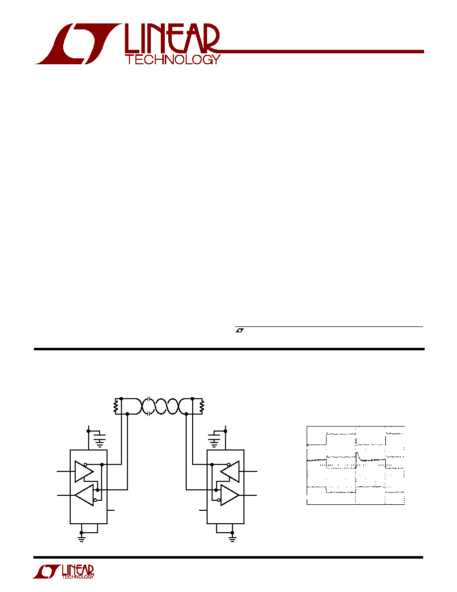
Fault Protected CAN Bus Network
R
T
120
1796 TA01
R
T
120
D
LT1796
TXD
5V
RXD
V
REF
R
S
GND
R
0.1
µ
F
7
1
4
6
5
2
8
D
LT1796
TXD
5V
RXD
V
REF
R
S
GND
R
0.1
µ
F
7
1
4
6
5
2
8
125kbps CANH and CANL Driver Output
CANH-CANL
2V/DIV
CANH
2V/DIV
CANL
2V/DIV
TXD IN
5V/DIV
5V/DIV
1796 TA02
2
LT1796
1796f
ORDER PART
NUMBER
(Note 1)
Supply Voltage (V
CC
) .............................................. 44V
R
S
Slope Control Input Voltage ................ 0.3V to 44V
V
REF
Reference Output Pin ......................... 0.3V to 7V
Driver Input Voltage .................................. 0.3V to 44V
CANH, CANL Data Line Pins ...................... 80V to 80V
Receiver Output Voltages ............................ 0.3V to 7V
Operating Temperature Range
LT1796C .................................................. 0
°
C to 70
°
C
LT1796I .............................................. 40
°
C to 85
°
C
Storage Temperature Range ................. 65
°
C to 150
°
C
Lead Temperature (Soldering, 10 sec).................. 300
°
C
LT1796CN8
LT1796CS8
LT1796IN8
LT1796IS8
T
JMAX
= 150
°
C,
JA
= 130
°
C/W (N8)
T
JMAX
= 150
°
C,
JA
= 150
°
C/W (S8)
ABSOLUTE
M
AXI
M
U
M
RATINGS
W
W
W
U
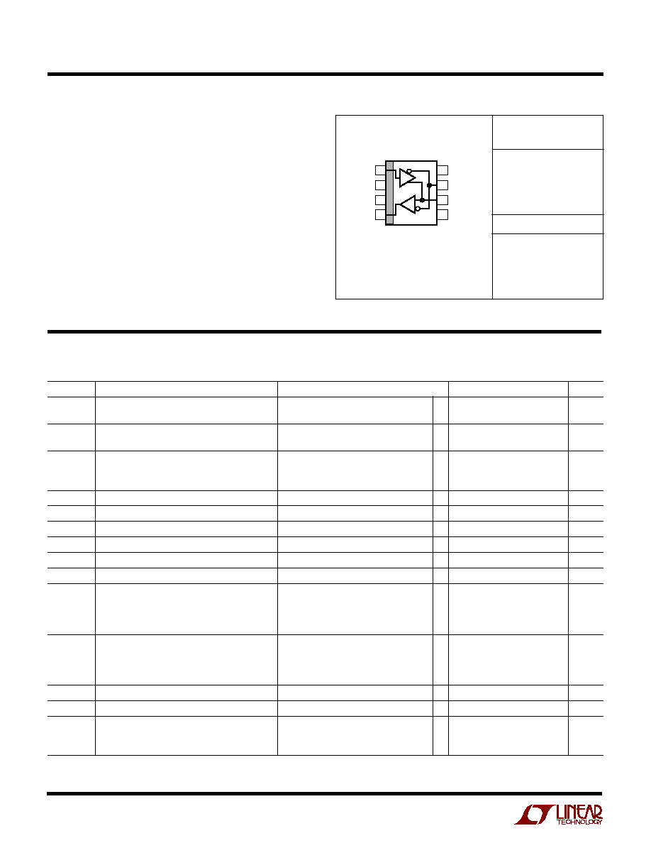
PACKAGE/ORDER I
N
FOR
M
ATIO
N
W
U
U
S8 PART MARKING
1796
1796I
1
2
3
4
8
7
6
5
TOP VIEW
R
S
CANH
CANL
V
REF
TXD
GND
V
CC
RXD
S8 PACKAGE
8-LEAD PLASTIC SO
N8 PACKAGE
8-LEAD PDIP
D
R
DC ELECTRICAL CHARACTERISTICS
The
q
denotes the specifications which apply over the full operating
temperature range, otherwise specifications are at T
A
= 25
°
C. V
CC
= 4.75V to 5.25V, V
RS
= 0V unless otherwise noted.
SYMBOL
PARAMETER
CONDITIONS
MIN
TYP
MAX
UNITS
V
CANH
CANH Output Voltage
V
TXD
= 0V, No Load
q
3.8
4.4
5.0
V
V
TXD
= 0V, R
L
= 60
q
2.8
3.5
4.6
V
V
CANL
CANL Output Voltage
V
TXD
= 0V, No Load
q
0
0.5
0.9
V
V
TXD
= 0V, R
L
= 60
q
0
1.3
1.6
V
V
OD
Dominant State Differential Output Voltage
V
TXD
= 0V, No Load, V
CC
= 4.75V
q
3.0
3.6
5.0
V
V
TXD
= 0V, R
L
= 60
, V
CC
= 4.75V
q
1.5
2.0
4.2
V
V
TXD
= 0V, R
L
= 36
, V
CC
= 4.75V
q
1.2
1.7
4.2
V
V
REC
Recessive State Differential Output Voltage
V
TXD
= 5V, R
L
= 60
q
10
0
10
mV
V
CMR
Recessive State Common Mode Output Voltage
V
TXD
= 5V, R
L
= 60
, V
CC
= 5V
q
2.7
3
3.5
V
V
CMD
Dominant State Common Mode Output Voltage
R
L
= 60
, V
CC
= 5V
q
2
2.5
3
V
V
IH
TXD Input High Voltage
q
2.8
V
V
IL
TXD Input Low Voltage
q
2
V
I
IN1
TXD Input Current
0 < V
TXD
< V
CC
q
5
5
µ
A
I
SCH
CANH Short-Circuit Current, Dominant Mode
V
CANH
= 0V, V
CC
= 5.25V
q
250
60
mA
V
CANH
= 36V, V
CC
= 5.25V
q
10
1
0
mA
V
CANH
= 60V, V
CC
= 5.25V
q
10
1
0
mA
V
CANH
= 60V, V
CC
= 5.25V
q
0
1
10
mA
I
SCL
CANL Short-Circuit Current, Dominant Mode
V
CANL
= 5V, V
TXD
= 0V, V
CC
= 5.25V
q
60
250
mA
V
CANL
= 36V, V
TXD
= 0V, V
CC
= 5.25V
q
0
1
10
mA
V
CANL
= 60V, V
TXD
= 0V, V
CC
= 5.25V
q
0
1
10
mA
V
CANL
= 60V, V
TXD
= 0V, V
CC
= 5.25V
q
10
1
0
mA
R
IND
Differential Input Resistance
V
TXD
= 5V, 7V < V
CANH
, V
CANL
< 12V
q
140
240
350
k
CANH, CANL Input Resistance
V
TXD
= 5V, 7V < V
CANH
, V
CANL
< 12V
q
70
120
175
k
Input Fault Current (CANH, CANL)
V
RS
= 5V, 60V < V
CANH
, V
CANL
< 60V
q
3
3
mA
V
TXD
= 5V, 60V < V
CANH
, V
CANL
< 60V
q
3
3
mA
V
CC
= 0V, 60V < V
CANH
, V
CANL
< 60V
q
3
3
mA
Consult LTC Marketing for parts specified with wider operating temperature ranges.
3
LT1796
1796f
DC ELECTRICAL CHARACTERISTICS
The
q
denotes the specifications which apply over the full operating
temperature range, otherwise specifications are at T
A
= 25
°
C. V
CC
= 4.75V to 5.25V, V
RS
= 0V unless otherwise noted.
SYMBOL
PARAMETER
CONDITIONS
MIN
TYP
MAX
UNITS
V
TH
Differential Input Threshold Voltage
V
RS
= 0V, 7V < V
CM
< 12V
q
0.5
0.9
V
for Receiver
V
RS
= 5V, 7V < V
CM
< 12V
q
0.5
0.9
V
V
TH
Receiver Input Hysteresis
7V < V
CM
< 12V
70
mV
V
OH
Receiver Output High Voltage
V
CC
= 4.75V, I
O
= 400
µ
A, V
ID
= 500mV
q
3
3.6
V
V
OL
Receiver Output Low Voltage
V
CC
= 4.75V, I
O
= 1.6mA, V
ID
= 900mV
q
0.15
0.4
V
I
SCR
Receiver Short-Circuit Current
0V < V
O
< V
CC
, V
CC
= 5.25V
q
7
20
85
mA
V
REF
Reference Output Voltage
100
µ
A < I
REF
< 100
µ
A
q
2.25
2.5
2.7
V
V
REFSC
Reference Output Short-Circuit Current
0 < V
REF
< V
CC
q
20
20
mA
V
RSSB
R
S
Pin Standby Threshold
V
CC
= 5V
q
2.5
2.8
4
V
I
RS
R
S
Input Current
V
RS
= 5V, V
CC
= 5V
q
0.1
10
µ
A
V
RS
= 0V, V
CC
= 5V
q
270
200
140
µ
A
R
S
= 47k, V
CC
= 5V
q
90
60
40
µ
A
I
CC
Supply Current
Dominant
No Load, V
RS
= 0V, V
TXD
= 0V, V
CC
= 5.25V
q
4.3
7
mA
Recessive
R
L
= 60
, V
RS
= 0V, V
TXD
= 5V, V
CC
= 5.25V
q
3.8
7
mA
Standby
R
L
= 60
, V
RS
= 5V, V
CC
= 5.25V
q
0.8
1.5
mA
SWITCHI G CHARACTERISTICS
U
The
q
denotes the specifications which apply over the full operating
temperature range. V
RS
= 0V unless otherwise noted. (Note 2)
SYMBOL
PARAMETER
CONDITIONS
MIN
TYP
MAX
UNITS
t
BIT
Minimum Bit Time
(Note 3)
q
8
µ
s
F
MAX
Maximum Data Rate
(Note 3)
q
125
kbps
t
TXDON
Driver Input to Bus Active
Figures 1, 2
R
S
= 0k
q
300
500
ns
R
S
= 47k
q
350
1000
ns
t
TXDOFF
Driver Input to Bus Inactive
Figures 1, 2
R
S
= 0k
q
500
1000
ns
R
S
= 47k
q
600
1500
ns
t
LBON
Loopback Delay Active
Figures 1, 3
q
0.6
1.5
µ
s
t
LBOFF
Loopback Delay Inactive
Figures 1, 3
q
1.5
3
µ
s
t
RXDOFF
Receiver Delay Off
Figures 1, 4
q
400
600
ns
t
RXDON
Receiver Delay On
Figures 1, 4
q
300
600
ns
t
RXDOFFSB
Receiver Delay Off, Standby
V
RS
= 4V, Figures 1, 4
q
1.5
4
µ
s
t
RXDONSB
Receiver Delay On, Standby
V
RS
= 4V, Figures 1, 4
q
1
4
µ
s
t
WAKE
Wake-Up Delay from Standby
Figures 1, 5
q
1
15
µ
s
SR
+
Positive Slew Rate
R
S
= 0k
q
5
12
65
V/
µ
s
R
S
= 47k
q
2
7
30
V/
µ
s
SR
Negative Slew Rate
R
S
= 0k
q
5
36
65
V/
µ
s
R
S
= 47k
q
2
5
15
V/
µ
s
Note 1: Absolute Maximum Ratings are those values beyond which the life
of the device may be impaired.
Note 2: Unless otherwise specified, testing done at V
CC
= 5V, T
A
= 25
°
C.
Note 3: Bit time and data rate specifications are guaranteed by driver and
receiver delay time measurements.
4
LT1796
1796f
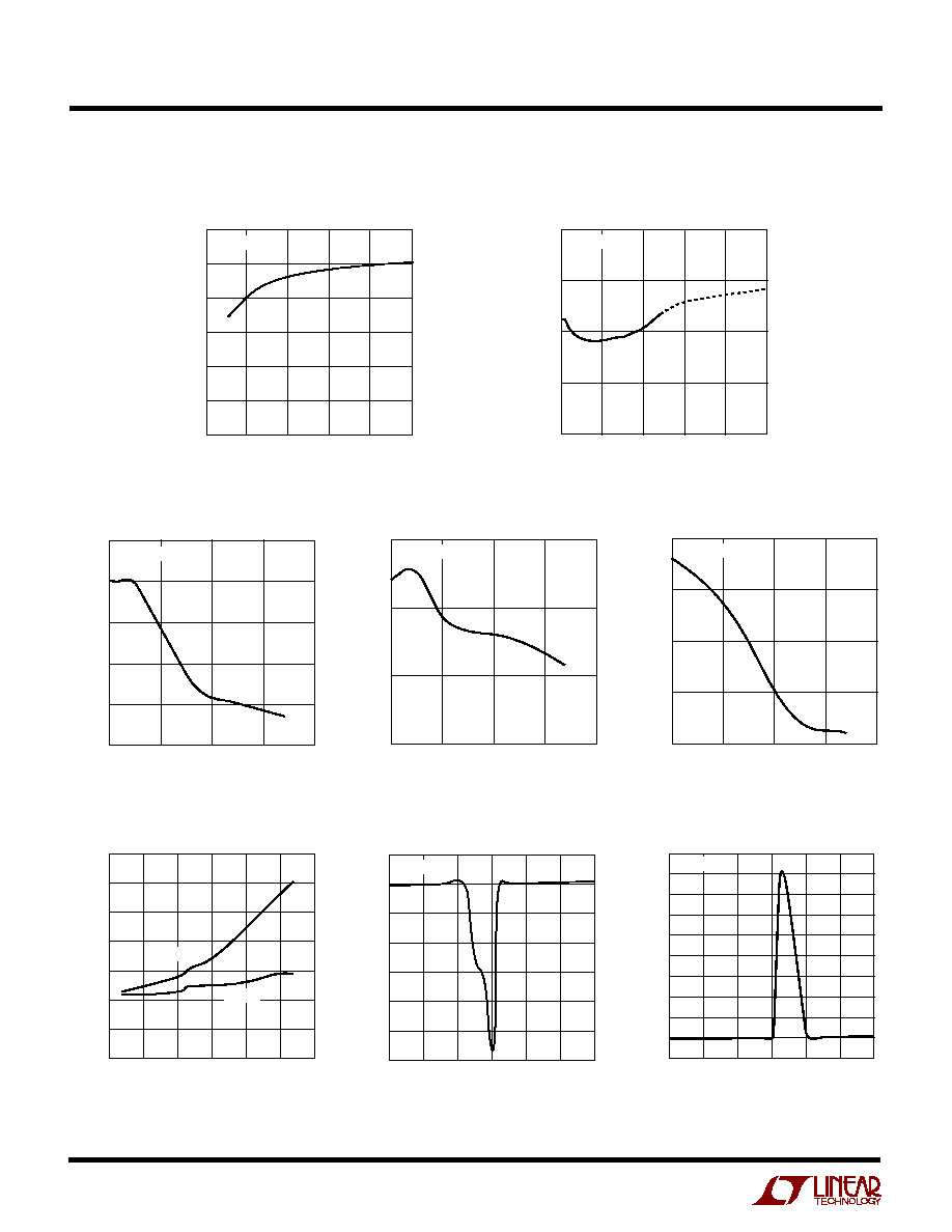
TYPICAL PERFOR A CE CHARACTERISTICS
U
W
Dominant State Bus Voltage
vs R
L
Supply Current vs Data Rate
Transmitting, 50% Duty Cycle
R
S
Pin Current vs R
S
Positive Slew Rate vs R
S
Negative Slew Rate vs R
S
Transmitter Propagation Delay vs
Temperature
CANH Short-Circuit Current vs
Voltage
CANL Short-Circuit Current vs
Voltage
V
CANL
(V)
I
SC
(mA)
90
80
70
60
50
40
30
20
10
0
10
1796 G09
60
40
20
0
20
40
60
T
A
= 25
°
C
R
L
(
)
0
V
OD
(V)
3.0
2.5
2.0
1.5
1.0
0.5
0
50
100
150
200
1796 G01
250
T
A
= 25
°
C
R
S
(k
)
0
SLEW CONTROL CURRENT (
µ
A)
250
200
150
100
50
0
1796 G04
20
40
80
60
T
A
= 25
°
C
R
S
(k
)
80
1796 G05
20
40
60
0
SR
+
(V/
µ
s)
10
15
5
0
T
A
= 25
°
C
R
S
(k
)
0
SR
(V/
µ
s)
20
30
80
1796 G06
10
0
20
40
60
40
T
A
= 25
°
C
TEMPERATURE (
°
C)
t
TXDOFF
AND t
TXDON
(ns)
700
600
500
400
300
200
100
0
1796 G07
50
25
0
25
50
75
100
t
TXDOFF
t
TXDON
V
CANH
(V)
I
SC
(mA)
20
0
20
40
60
80
100
120
1796 G08
60
40
20
0
20
40
60
T
A
= 25
°
C
DATA RATE (Kbps)
0
SUPPLY CURRENT (mA)
22
23
200
1796 G03
21
20
50
100
150
250
24
T
A
= 25
°
C
5
LT1796
1796f
U
U
U
PI FU CTIO S
TXD (Pin 1): Driver Input. Logic-level thresholds are set by
V
REF
. A logic input level higher than V
REF
turns the driver
outputs off, releasing control of the CANH and CANL lines.
A logic input less than V
REF
turns the driver outputs on,
pulling CANH high and CANL low. An open TXD input will
float high, turning the driver outputs off. The TXD input pin
can withstand voltages from 0.3V to 44V with no dam-
age.
GND (Pin 2): Ground.
V
CC
(Pin 3): Positive Supply Input. Normal operation is
with a 4.75V to 5.25V supply. Operation with supplies up
to 44V is possible with unterminated bus lines. Operation
at high voltages with normally terminated busses will
result in excessive power dissipation and activation of the
thermal shutdown circuit. V
CC
should be decoupled with
a 0.1
µ
F low ESR capacitor placed as close to the supply pin
as possible.
RXD (Pin 4): Receiver TTL Level-Logic Output. A high level
output indicates a recessive state (zero-volt differential)
bus. A dominant state forces a low receiver output.
V
REF
(Pin 5): Reference Output. The reference voltage sets
the TXD input threshold and the recessive bus common
mode voltage at CANH and CANL. V
REF
is approximately
V
CC
/2 for low voltage operation. When V
CC
> 7.5V, V
REF
maintains a 3.5V level.
CANL (Pin 6): CAN Bus Low Data Line. The CANL pin is one
input to the receiver and the low driver output. In the
dominant state (TXD low), the driver pulls the CANL pin to
within 1V of GND. In the recessive state (TXD high), the
driver output stays high impedance. The CANL pin is
protected from voltage faults from 60V to 60V in domi-
nant, recessive, standby or powered off modes. On-chip
ESD protection meets IEC-1000-4-2 levels.
CANH (Pin 7): CAN Bus High Data Line. The CANH pin is
one input to the receiver and the high driver output. In the
dominant state (TXD low), the driver pulls the CANH pin to
within 1V of V
CC
. In the recessive state (TXD high), the
driver output stays high impedance. The CANH pin is
protected from voltage faults from 60V to 60V in domi-
nant, recessive, standby or powered off modes. On-chip
ESD protection meets IEC-1000-4-2 levels.
R
S
(Pin 8): Slope Control. This pin is a multifunction
control pin. When R
S
is high (V
RS
> 4V), the circuit goes
into a low power standby mode. In standby, the driver
always stays in a high impedance (recessive) state. The
receiver operates in a low power (slow) monitoring mode.
Received data may be used to "wake-up" the system to full
functionality. Full speed normal operation occurs if R
S
is
tied low through a resistance of less than 3k. The current
out of R
S
will be limited to about 500
µ
A in the low state.
Controlling the current out of R
S
with a resistor greater
than 3k or by using a current source allows slew rate
control of the data output onto CANH and CANL.
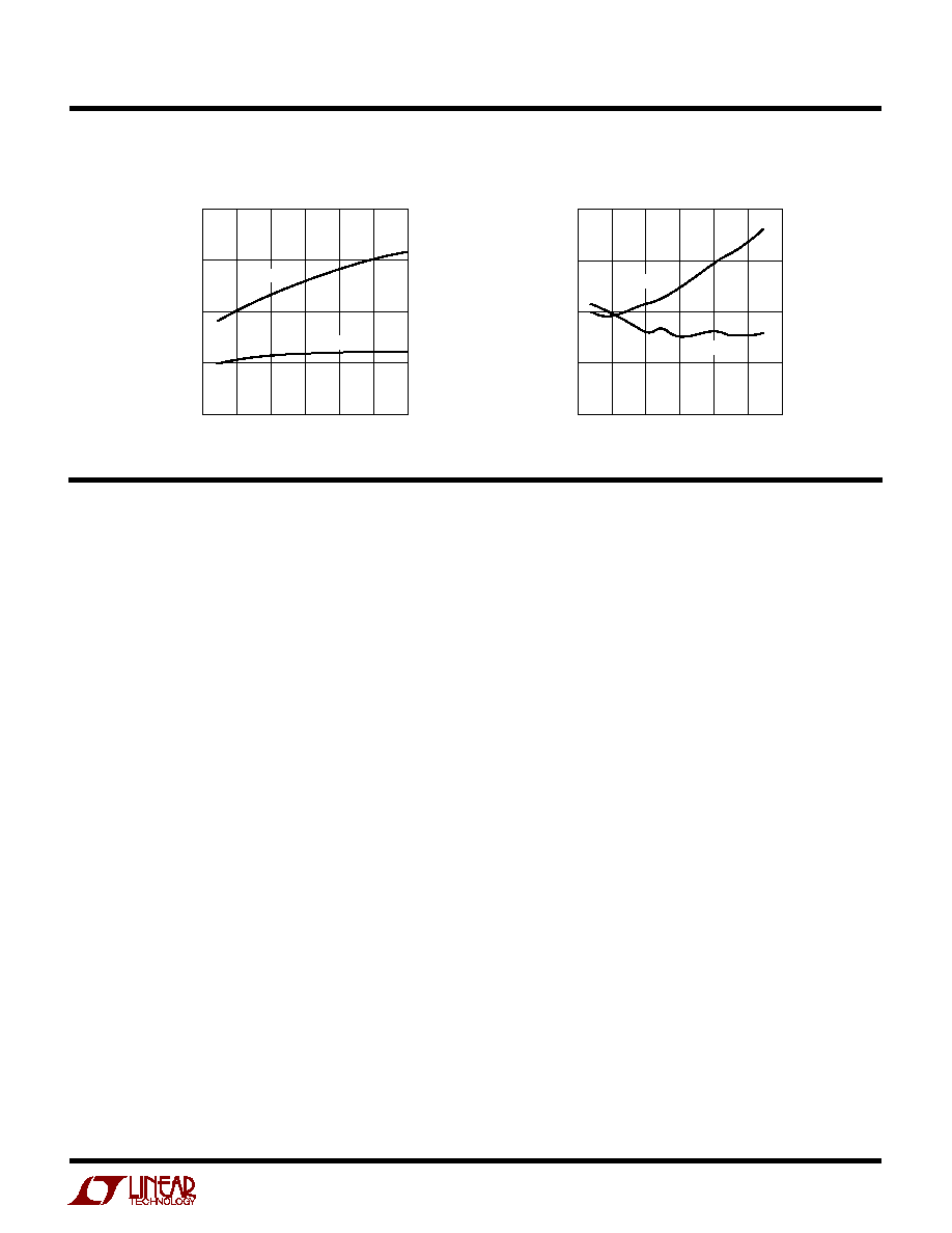
TYPICAL PERFOR A CE CHARACTERISTICS
U
W
Receiver Thresholds vs
Temperature
Receiver Propagation Delay vs
Temperature
TEMPERATURE (
°
C)
50
V
TH
(V)
0.80
0.75
0.70
0.65
0.60
25
0
25
50
1796 G10
75
100
V
TH
RISING
V
TH
FALLING
TEMPERATURE (
°
C)
t
RXDOFF
AND t
RXDON
(ns)
400
350
300
250
200
1796 G11
50
25
0
25
50
75
100
t
RXDOFF
t
RXDON