 | ÐлекÑÑоннÑй компоненÑ: LT1885 | СкаÑаÑÑ:  PDF PDF  ZIP ZIP |
Äîêóìåíòàöèÿ è îïèñàíèÿ www.docs.chipfind.ru
LT1884/LT1885
1
The LT
®
1884/LT1885 op amps bring high accuracy input
performance to amplifiers with rail-to-rail output swing
while providing faster response than other precision am-
plifiers. Input offset voltage is trimmed to less than 50
µ
V
and the low drift maintains this accuracy over the operat-
ing temperature range. Input bias currents are an ultralow
400pA maximum.
The amplifiers work on any total power supply voltage
between 2.7V and 36V (fully specified from 5V to
±
15V).
Output voltage swings to within 40mV of the negative
supply and 220mV of the positive supply make these
amplifiers good choices for low voltage single supply
operation.
Slew rates of 1V/
µ
s with a supply current of less than 1mA
per amplifier give superior response and settling time
performance in a low power precision amplifier.
The dual LT1884 is available with standard pinouts in
8-pin SO and PDIP packages. The quad LT1885 is also in
the standard pinout 14-pin SO package.
s
Thermocouple Amplifiers
s
Bridge Transducer Conditioners
s
Instrumentation Amplifiers
s
Battery-Powered Systems
s
Photo Current Amplifiers
s
Precision Integrators
s
Precision Current Sources
, LTC and LT are registered trademarks of Linear Technology Corporation.
s
Offset Voltage: 50
µ
V Max (LT1884A)
s
Input Bias Current: 400pA Max (LT1884A)
s
Offset Voltage Drift: 0.8
µ
V/
°
C Max
s
Rail-to-Rail Output Swing
s
Operates with Single or Split Supplies
s
Open-Loop Voltage Gain: 1 Million Min
s
1mA Maximum Supply Current Per Amplifier
s
Slew Rate: 1V/
µ
s
s
Standard Pinouts
Dual/Quad Rail-to-Rail
Output, Picoamp Input
Precision Op Amps
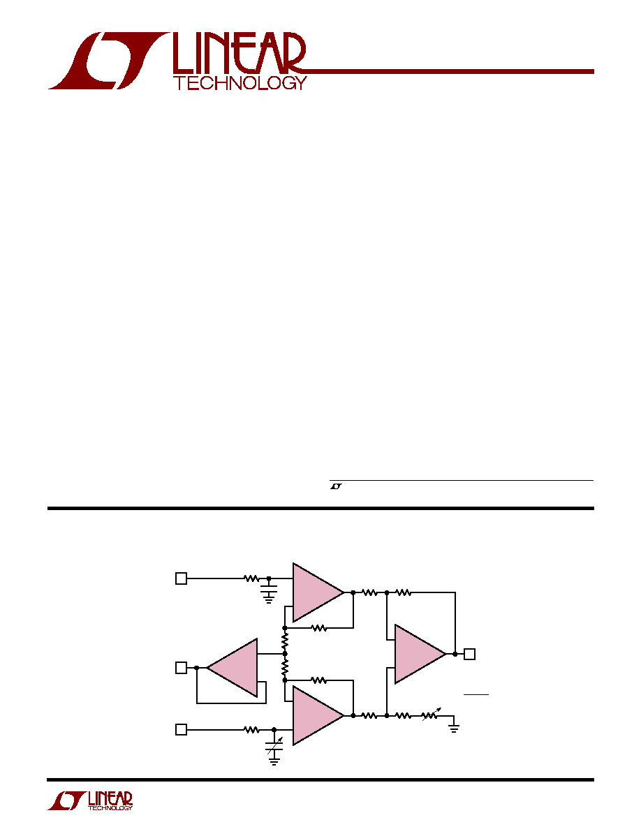
Input Fault Protected Instrumentation Amplifier
FEATURES
DESCRIPTIO
U
APPLICATIO S
U
TYPICAL APPLICATIO
U
+
+
+
+
1884 TA01
R
G/2
R
G/2
22pF
TRIM FOR
AC CMRR
10k
1/4 LT1885
OUT
IN
GUARD
+IN
1/4 LT1885
1/4 LT1885
1/4 LT1885
10k
1M
1M
3
5
10k
10k
9.76k
500
TRIM FIRST
FOR DC CMRR
10k
GAIN =
2·10k
R
G
10pF
LT1884/LT1885
2
Supply Voltage (V
+
to V
) ....................................... 40V
Differential Input Voltage (Note 2) .........................
±
10V
Input Voltage .................................................... V
+
to V
Input Current (Note 2) ........................................
±
10mA
Output Short-Circuit Duration (Note 3) ............ Indefinite
ORDER
PART NUMBER
S8 PART MARKING
T
JMAX
= 150
°
C,
JA
= 130
°
C/W (N8)
T
JMAX
= 150
°
C,
JA
= 190
°
C/W (S8)
Consult factory for Military grade parts.
1884
1884A
LT1885CS
LT1885IS
(Note 1)
ABSOLUTE AXI U RATI GS
W
W
W
U
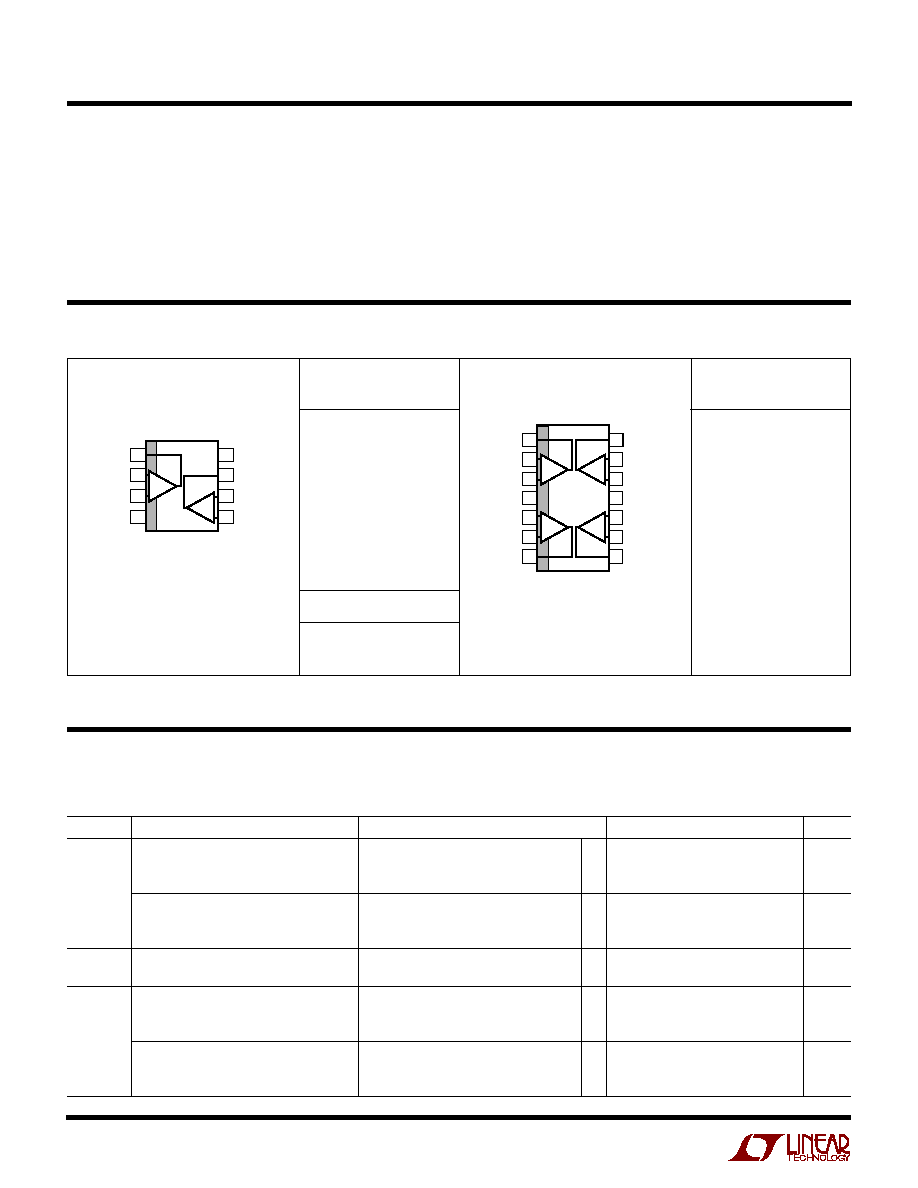
PACKAGE/ORDER I FOR ATIO
U
U
W
Operating Temperature Range (Note 4) .. 40
°
C to 85
°
C
Specified Temperature Range (Note 5) ... 40
°
C to 85
°
C
Maximum Junction Temperature .......................... 150
°
C
Storage Temperature Range ................. 65
°
C to 150
°
C
Lead Temperature (Soldering, 10 sec).................. 300
°
C
1884I
1884AI
ORDER
PART NUMBER
LT1884CN8
LT1884CS8
LT1884ACN8
LT1884ACS8
LT1884IN8
LT1884IS8
LT1884AIN8
LT1884AIS8
1
2
3
4
8
7
6
5
TOP VIEW
V
+
OUT B
IN B
+IN B
OUT A
IN A
+IN A
V
S8 PACKAGE
8-LEAD PLASTIC SO
N8 PACKAGE
8-LEAD PDIP
A
B
TOP VIEW
S PACKAGE
14-LEAD PLASTIC SO
1
2
3
4
5
6
7
14
13
12
11
10
9
8
OUT A
IN A
+IN A
V
+
+IN B
IN B
OUT B
OUT D
IN D
+IN D
V
+IN C
IN C
OUT C
A
D
C
B
T
JMAX
= 150
°
C,
JA
= 110
°
C/W
The
q
denotes the specifications which apply over the full operating temperature range, otherwise specifications are at T
A
= 25
°
C.
Single supply operation V
EE
= 0, V
CC
= 5V; V
CM
= V
CC
/2 unless otherwise noted. (Note 5)
SYMBOL
PARAMETER
CONDITIONS
MIN
TYP
MAX
UNITS
V
OS
Input Offset Voltage (LT1884A)
25
50
µ
V
0
°
C < T
A
< 70
°
C
q
85
µ
V
40
°
C < T
A
< 85
°
C
q
110
µ
V
Input Offset Voltage (LT1884/LT1885)
30
80
µ
V
0
°
C < T
A
< 70
°
C
q
125
µ
V
40
°
C < T
A
< 85
°
C
q
150
µ
V
Input Offset Voltage Drift (Note 6)
0
°
C < T
A
< 70
°
C
q
0.3
0.8
µ
V/
°
C
40
°
C < T
A
< 85
°
C
q
0.3
0.8
µ
V/
°
C
I
OS
Input Offset Current (LT1884A)
100
300
pA
0
°
C < T
A
< 70
°
C
q
400
pA
40
°
C < T
A
< 85
°
C
q
500
pA
Input Offset Current (LT1884/LT1885)
150
900
pA
0
°
C < T
A
< 70
°
C
q
1200
pA
40
°
C < T
A
< 85
°
C
q
1400
pA
ELECTRICAL CHARACTERISTICS
LT1884/LT1885
3
The
q
denotes the specifications which apply over the full operating temperature range, otherwise specifications are at T
A
= 25
°
C.
Single supply operation V
EE
= 0, V
CC
= 5V; V
CM
= V
CC
/2 unless otherwise noted. (Note 5)
SYMBOL
PARAMETER
CONDITIONS
MIN
TYP
MAX
UNITS
I
B
Input Bias Current (LT1884A)
100
400
pA
0
°
C < T
A
< 70
°
C
q
500
pA
40
°
C < T
A
< 85
°
C
q
600
pA
Input Bias Current (LT1884/LT1885)
150
900
pA
0
°
C < T
A
< 70
°
C
q
1200
pA
40
°
C < T
A
< 85
°
C
q
1400
pA
Input Noise Voltage
0.1Hz to 10Hz
0.4
µ
V
P-P
e
n
Input Noise Voltage Density
f = 1kHz
9.5
nV/
Hz
i
n
Input Noise Current Density
f = 1kHz
0.05
pA/
Hz
V
CM
Input Voltage Range
V
EE
+ 1.0
V
CC
1.0
V
q
V
EE
+ 1.2
V
CC
1.2
V
CMRR
Common Mode Rejection Ratio
1V < V
CM
< 4V
108
128
dB
1.2V < V
CM
< 3.8V
q
106
dB
PSRR
Power Supply Rejection Ratio
V
EE
= 0, V
CM
= 1.5V; 2.7V < V
CC
< 32V
q
108
132
dB
Minimum Operating Supply Voltage
q
2.4
2.7
V
A
VOL
Large-Signal Voltage Gain
R
L
= 10k; 1V < V
OUT
< 4V
500
1600
V/mV
q
350
V/mV
R
L
= 2k; 1V < V
OUT
< 4V
400
800
V/mV
q
300
V/mV
R
L
= 1k; 1V < V
OUT
< 4V
300
400
V/mV
q
200
V/mV
V
OL
Output Voltage Swing Low
No Load
q
20
40
mV
I
SINK
= 100
µ
A
q
25
50
mV
I
SINK
= 1mA
q
70
150
mV
I
SINK
= 5mA
q
270
600
mV
V
OH
Output Voltage Swing High
No Load
q
120
220
mV
(Referred to V
CC
)
I
SOURCE
= 100
µ
A
q
130
230
mV
I
SOURCE
= 1mA
q
180
300
mV
I
SOURCE
= 5mA
q
360
600
mV
I
S
Supply Current per Amplifier
V
CC
= 3V
0.45
0.65
0.85
mA
q
1.30
mA
V
CC
= 5V
0.50
0.65
0.9
mA
q
1.4
mA
V
CC
= 12V
0.50
0.70
1.0
mA
q
1.5
mA
I
SC
Short-Circuit Current
V
OUT
Short to GND
q
15
30
mA
V
OUT
Short to V
CC
q
15
30
mA
GBW
Gain-Bandwidth Product
f = 20kHz
1.2
2
MHz
t
S
Settling Time
0.01%, V
OUT
= 1.5V to 3.5V,
10
µ
s
A
V
= 1, R
L
= 2k
SR
+
Positive Slew Rate
A
V
= 1
0.45
0.9
V/
µ
s
q
0.36
V/
µ
s
SR
Negative Slew Rate
A
V
= 1
0.35
0.7
V/
µ
s
q
0.25
V/
µ
s
ELECTRICAL CHARACTERISTICS
LT1884/LT1885
4
The
q
denotes the specifications which apply over the full operating temperature range, otherwise specifications are at T
A
= 25
°
C.
Single supply operation V
EE
= 0, V
CC
= 5V; V
CM
= V
CC
/2 unless otherwise noted. (Note 5)
SYMBOL
PARAMETER
CONDITIONS
MIN
TYP
MAX
UNITS
V
OS
Offset Voltage Match (LT1884A)
30
70
µ
V
0
°
C < T
A
< 70
°
C
q
125
µ
V
40
°
C < T
A
< 85
°
C
q
160
µ
V
Offset Voltage Match (LT1884/LT1885)
(Note 7)
35
125
µ
V
0
°
C < T
A
< 70
°
C
q
195
µ
V
40
°
C < T
A
< 85
°
C
q
235
µ
V
Offset Voltage Match Drift
(Notes 6, 7)
q
0.4
1.2
µ
V/
°
C
I
B
+
Noninverting Bias Current Match
200
600
pA
(LT1884A)
0
°
C < T
A
< 70
°
C
q
700
pA
40
°
C < T
A
< 85
°
C
q
850
pA
Noninverting Bias Current Match
(Notes 7, 9)
250
1200
pA
(LT1884/LT1885)
0
°
C < T
A
< 70
°
C
q
1600
pA
40
°
C < T
A
< 85
°
C
q
1900
pA
CMRR
Common Mode Rejection Match
(Notes 7, 9)
q
104
125
dB
PSRR
Positive Power Supply Rejection Match
V
EE
= 0V, V
CM
= 1.5V, 2.7V < V
CC
< 32V,
q
104
126
dB
(Notes 7, 9)
ELECTRICAL CHARACTERISTICS
The
q
denotes the specifications which apply over the full operating temperature range, otherwise specifications are at T
A
= 25
°
C.
Split supply operation V
S
=
±
15V; V
CM
= 0V unless otherwise noted. (Note 5)
SYMBOL
PARAMETER
CONDITIONS
MIN
TYP
MAX
UNITS
V
OS
Input Offset Voltage (LT1884A)
25
50
µ
V
0
°
C < T
A
< 70
°
C
q
85
µ
V
40
°
C < T
A
< 85
°
C
q
110
µ
V
Input Offset Voltage (LT1884/LT1885)
30
80
µ
V
0
°
C < T
A
< 70
°
C
q
125
µ
V
40
°
C < T
A
< 85
°
C
q
150
µ
V
Input Offset Voltage Drift (Note 6)
0
°
C < T
A
< 70
°
C
q
0.3
0.8
µ
V/
°
C
40
°
C < T
A
< 85
°
C
q
0.3
0.8
µ
V/
°
C
I
OS
Input Offset Current (LT1884A)
150
300
pA
0
°
C < T
A
< 70
°
C
q
400
pA
40
°
C < T
A
< 85
°
C
q
500
pA
Input Offset Current (LT1884/LT1885)
150
900
pA
0
°
C < T
A
< 70
°
C
q
1200
pA
40
°
C < T
A
< 85
°
C
q
1400
pA
I
B
Input Bias Current (LT1884A)
150
400
pA
0
°
C < T
A
< 70
°
C
q
500
pA
40
°
C < T
A
< 85
°
C
q
600
pA
Input Bias Current (LT1884/LT1885)
150
900
pA
0
°
C < T
A
< 70
°
C
q
1200
pA
40
°
C < T
A
< 85
°
C
q
1400
pA
Input Noise Voltage
0.1Hz to 10Hz
0.4
µ
V
P-P
e
n
Input Noise Voltage Density
f = 1kHz
9.5
nV/
Hz
i
n
Input Noise Current Density
f = 1kHz
0.05
pA/
Hz
V
CM
Input Voltage Range
V
EE
+ 1.0
V
CC
1.0
V
q
V
EE
+ 1.2
V
CC
1.2
V
CMRR
Common Mode Rejection Ratio
13.5V < V
CM
< 13.5V
q
114
130
dB
LT1884/LT1885
5
SYMBOL
PARAMETER
CONDITIONS
MIN
TYP
MAX
UNITS
+ PSRR
Positive Power Supply Rejection Ratio
V
EE
= 15V, V
CM
= 0V; 1.5V < V
CC
< 18V
q
114
132
dB
PSRR
Negative Power Supply Rejection Ratio
V
CC
= 15V, V
CM
= 0V; 1.5V < V
EE
< 18V
q
106
132
dB
Minimum Operating Supply Voltage
q
±
1.2
±
1.35
V
A
VOL
Large-Signal Voltage Gain
R
L
= 10k; 13.5V < V
OUT
< 13.5V
1000
1600
V/mV
q
700
V/mV
R
L
= 2k; 13.5V < V
OUT
< 13.5V
250
420
V/mV
q
175
V/mV
R
L
= 1k; 12V < V
OUT
< 12V
100
230
V/mV
q
75
V/mV
V
OL
Output Voltage Swing Low
No Load
q
20
40
mV
(Referred to V
EE
)
I
SINK
= 100
µ
A
q
25
50
mV
I
SINK
= 1mA
q
70
150
mV
I
SINK
= 5mA
q
270
600
mV
V
OH
Output Voltage Swing High
No Load
q
160
220
mV
(Referred to V
CC
)
I
SOURCE
= 100
µ
A
q
160
230
mV
I
SOURCE
= 1mA
q
180
300
mV
I
SOURCE
= 5mA
q
360
600
mV
I
S
Supply Current Per Amplifier
V
S
=
±
15V
0.85
1.1
mA
q
1.6
mA
I
SC
Short-Circuit Current
V
OUT
Short to V
EE
q
15
50
mA
V
OUT
Short to V
CC
q
15
30
mA
GBW
Gain-Bandwidth Product
f = 20kHz
1.5
2.2
MHz
t
S
Settling Time
0.01%, V
OUT
= 5V to 5V,
17
µ
s
A
V
= 1, R
L
= 2k
SR
+
Positive Slew Rate
A
V
= 1
0.5
1.0
V/
µ
s
q
0.4
V/
µ
s
SR
Negative Slew Rate
A
V
= 1
0.40
0.7
V/
µ
s
q
0.26
V/
µ
s
V
OS
Offset Voltage Match (LT1884A)
(Note 7)
35
70
µ
V
0
°
C < T
A
< 70
°
C
q
125
µ
V
40
°
C < T
A
< 85
°
C
q
160
µ
V
Offset Voltage Match (LT1884/LT1885)
(Note 7)
35
125
µ
V
0
°
C < T
A
< 70
°
C
q
175
µ
V
40
°
C < T
A
< 85
°
C
q
235
µ
V
Offset Voltage Match Drift
(Note 6, 7)
q
0.4
1.1
µ
V/
°
C
I
B
+
Noninverting Bias Current Match
(Notes 7, 8)
200
600
pA
(LT1884A)
0
°
C < T
A
< 70
°
C
q
700
pA
40
°
C < T
A
< 85
°
C
q
850
pA
Noninverting Bias Current Match
(Notes 7, 8)
240
1200
pA
(LT1884/LT1885)
0
°
C < T
A
< 70
°
C
q
1600
pA
40
°
C < T
A
< 85
°
C
q
1900
pA
CMRR
Common Mode Rejection Match
(Notes 7, 9)
q
106
125
dB
+PSRR
Positive Power Supply Rejection Match
V
EE
= 15V, V
CM
= 0V, 1.5V < V
CC
< 18V,
q
108
124
dB
(Notes 7, 9)
PSRR
Negative Power Supply Rejection Match
V
CC
= 15V, V
CM
= 0V, 1.5V < V
EE
< 18V,
q
102
132
dB
(Notes 7, 9)
The
q
denotes the specifications which apply over the full operating temperature range, otherwise specifications are at T
A
= 25
°
C.
Split supply operation V
S
=
±
15V; V
CM
= 0V unless otherwise noted. (Note 5)
ELECTRICAL CHARACTERISTICS