 | ÐлекÑÑоннÑй компоненÑ: LT1910 | СкаÑаÑÑ:  PDF PDF  ZIP ZIP |
Äîêóìåíòàöèÿ è îïèñàíèÿ www.docs.chipfind.ru
1
LT1910
sn1910 1910fs
Protected High Side
MOSFET Driver
s
8V to 48V Power Supply Range
s
Protected from 15V to 60V Supply Transients
s
Short-Circuit Protected
s
Automatic Restart Timer
s
Open-Collector Fault Flag
s
Fully Enhances N-Channel MOSFET Switches
s
Programmable Current Limit, Delay Time and
Autorestart Period
s
Voltage Limited Gate Drive
s
Defaults to OFF State with Open Input
s
Available in SO-8 Package
s
Industrial Control
s
Avionics Systems
s
Automotive Switches
s
Stepper Motor and DC Motor Control
s
Electronic Circuit Breaker
, LTC and LT are registered trademarks of Linear Technology Corporation.
The LT
®
1910 is a high side gate driver that allows the use
of low cost N-channel power MOSFETs for high side
switching applications. It contains a completely self-con-
tained charge pump to fully enhance an N-channel MOSFET
switch with no external components.
When the internal drain comparator senses that the switch
current has exceeded the preset level, the switch is turned
off and a fault flag is asserted. The switch remains off for
a period of time set by an external timing capacitor and
then automatically attempts to restart. If the fault still
exists, this cycle repeats until the fault is removed, thus
protecting the MOSFET. The fault flag becomes inactive
once the switch restarts successfully.
The LT1910 has been specifically designed for harsh
operating environments such as industrial, avionics and
automotive applications where poor supply regulation
and/or transients may be present. The device will not
sustain damage from supply transients of 15V to 60V.
The LT1910 is available in the SO-8 package.
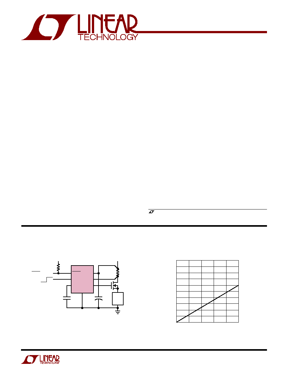
FAULT
IN
TIMER
V
+
SENSE
GATE
LT1910
5.1k
3
4
2
8
6
5
1
24V
5V
FAULT OUTPUT
OFF ON
GND
IRFZ34
1910 TA01
10
µ
F
50V
0.1
µ
F
0.01
LOAD
+
Fault Protected High Side Switch
LOAD CURRENT (A)
0
TOTAL DROP (V)
0.30
0.40
0.50
4
1910 TA02
0.20
0.10
0.25
0.35
0.45
0.15
0.05
0
1
2
3
5
Switch Drop vs Load Current
DESCRIPTIO
U
FEATURES
APPLICATIO S
U
TYPICAL APPLICATIO
U
2
LT1910
sn1910 1910fs
SYMBOL
PARAMETER
CONDITIONS
MIN
TYP
MAX
UNITS
I
S
Supply Current (OFF State)
V
+
= 48V, V
IN
= 0.8V
1.2
1.9
2.5
mA
I
S(ON)
Delta Supply Current (ON State)
V
IN
= 2V, Measure Increase in I
S
0.8
1.2
mA
V
INH
Input High Voltage
q
2
V
V
INL
Input Low Voltage
q
0.8
V
I
IN
Input Current
V
IN
= 2V
q
15
30
50
µ
A
V
IN
= 5V
q
55
110
185
µ
A
C
IN
Input Capacitance (Note 3)
5
pF
V
T(TH)
Timer Threshold Voltage
V
IN
= 2V, Adjust V
T
q
2.6
2.9
3.2
V
V
T(CL)
Timer Clamp Voltage
V
IN
= 0.8V
3.2
3.5
3.8
V
I
T
Timer Charge Current
V
IN
= V
T
= 2V
9
14
20
µ
A
V
SENSE
Drain Sense Threshold Voltage
50
65
80
mV
Temperature Coefficient (Note 3)
0.33
%/
°
C
I
SENSE
Drain Sense Input Current
V
+
= 48V, V
SENSE
= 65mV
0.5
1.5
µ
A
V
GATE
V
+
Gate Voltage Above Supply
V
+
= 8V
4
4.5
6
V
V
+
= 12V
q
7
8.5
10
V
V
+
= 24V
q
10
12
14
V
V
+
= 48V
q
10
12
14
V
V
F(TH)
FAULT Output High Threshold Voltage
V
IN
= 2V, I
F
= 1mA, Adjust V
T
3.1
3.4
3.7
V
FAULT Output Low Threshold Voltage
3.0
3.3
3.6
V
V
FOL
FAULT Output Low Voltage
I
F
= 1mA
q
0.07
0.4
V
t
ON
Turn-On Time
V
+
= 24V, V
GATE
= 32V, C
GATE
= 1nF
100
220
400
µ
s
t
OFF
Turn-Off Time
V
+
= 24V, V
GATE
= 2V, C
GATE
= 1nF
25
100
µ
s
t
OFF(CL)
Current Limit Turn-Off Time
V
+
= 24V, (V
+
V
SENSE
)
0.1V, C
GATE
= 1nF
20
50
µ
s
(Note 1)
Supply Voltage (Pin 8) ............................... 15V to 60V
Input Voltage (Pin 4) .................... (GND 0.3V) to 15V
GATE Voltage (Pin 5) .............................................. 75V
SENSE Voltage (Pin 6) ....................................... V
+
±
5V
FAULT Voltage (Pin 3) ............................................ 36V
Current (Pins 1, 2, 4, 5, 6, 8) ............................... 40mA
Operating Ambient Temperature Range
(Note 2) ...................................................40
°
C to 85
°
C
Junction Temperature Range ................ 40
°
C to 125
°
C
Storage Temperature Range ................. 65
°
C to 150
°
C
Lead Temperature (Soldering, 10 sec).................. 300
°
C
ABSOLUTE
M
AXI
M
U
M
RATINGS
W
W
W
U
PACKAGE/ORDER I
N
FOR
M
ATIO
N
W
U
U
ORDER PART
NUMBER
LT1910ES8
S8 PART MARKING
1910E
T
JMAX
= 125
°
C,
JA
= 150
°
C/W
The
q
denotes specifications that apply over the full operating temperature
range, otherwise specifications are at T
A
= 25
°
C. V
+
= 12V to 48V unless otherwise noted.
Consult LTC Marketing for parts specified with wider operating temperature ranges.
ELECTRICAL CHARACTERISTICS
1
2
3
4
8
7
6
5
TOP VIEW
V
+
NC
SENSE
GATE
GND
TIMER
FAULT
IN
S8 PACKAGE
8-LEAD PLASTIC SO
Note 1: Absolute Maximum Ratings are those values beyond which the life
of a device may be impaired.
Note 2: The LT1910E is guaranteed to meet performance specifications
from 0
°
C to 70
°
C. Specifications over the 40
°
C to 85
°
C operating
temperature range are assured by design, characterization and correlation
with statistical process controls.
Note 3: Guaranteed but not tested.
3
LT1910
sn1910 1910fs
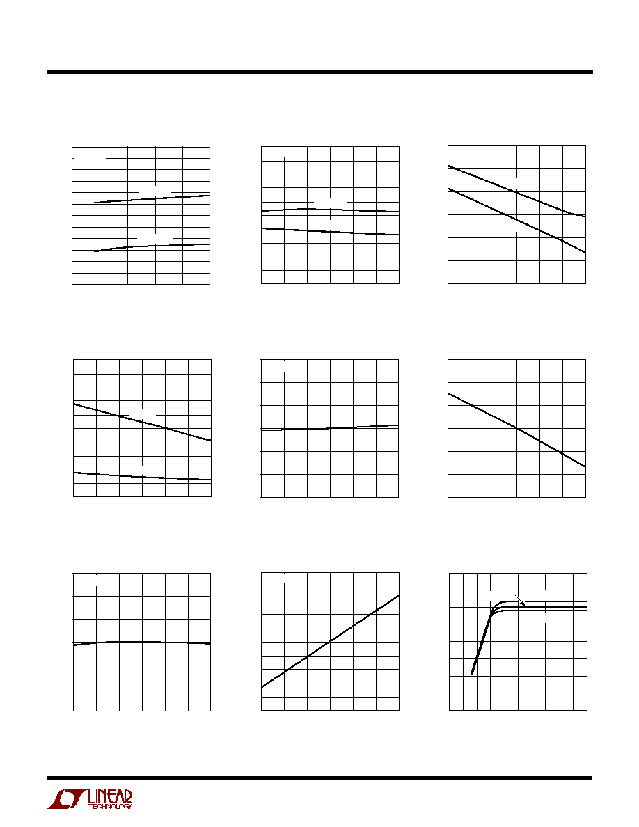
TYPICAL PERFOR A CE CHARACTERISTICS
U
W
Supply Current vs Supply Voltage
Supply Current vs Temperature
Input Voltage vs Temperature
Input Current vs Temperature
Timer Threshold Voltage
vs Temperature
Timer Clamp Voltage
vs Temperature
Timer Charge Current
vs Temperature
Drain Sense Threshold Voltage
vs Temperature
MOSFET Gate Voltage Above V
+
(V
GATE
V
+
) vs Supply Voltage
SUPPLY VOLTAGE (V)
0
SUPPLY CURRENT (mA)
2.4
2.8
3.2
3.6
40
1910 G01
2.0
1.6
2.2
2.6
3.0
3.4
1.8
1.4
1.2
10
20
30
50
ON STATE
OFF STATE
T
A
= 25
°
C
TEMPERATURE (
°
C)
50
0
SUPPLY CURRENT (mA)
1.0
2.0
3.0
2.5
25
0
25
50
1910 G02
75
4.0
5.0
0.5
1.5
3.5
4.5
100
V
+
= 48V
ON STATE
OFF STATE
TEMPERATURE (
°
C)
50
INPUT VOLTAGE (V)
1.0
1.2
1.4
1.6
2.0
25
0
25
50
1910 G03
75
100
1.8
0.8
V
INH
V
INL
TEMPERATURE (
°
C)
50
0
INPUT CURRENT (
µ
A)
40
80
120
25
0
25
50
1910 G04
75
160
200
20
60
100
140
180
100
V
IN
= 5V
V
IN
= 2V
TEMPERATURE (
°
C)
50
TIMER THRESHOLD VOLTAGE (V) 2.7
2.8
2.9
3.0
3.2
25
0
25
50
1910 G05
75
100
3.1
2.6
V
IN
= 2V
TEMPERATURE (
°
C)
50
TIMER CLAMP VOLTAGE (V)
3.3
3.4
3.5
3.6
3.8
25
0
25
50
1910 G06
75
100
3.7
3.2
V
IN
0.8V
TEMPERATURE (
°
C)
50
TIMER CHARGE CURRENT (
µ
A)
10
12
14
16
20
25
0
25
50
1910 G07
75
100
18
8
V
IN
= V
T
= 2V
TEMPERATURE (
°
C)
50
40
DRAIN SENSE THRESHOLD VOLTAGE (mV)
50
60
70
65
25
0
25
50
1910 G08
75
80
90
45
55
75
85
100
V
+
= 24V
SUPPLY VOLTAGE (V)
0
MOSFET GATE VOLTAGE ABOVE V
+
(V
GATE
V
+
) (V)
16
14
12
10
8
6
4
2
0
40
LTC1266 · F04
10
20
30
50
35
5
15
25
45
T
A
= 85
°
C
T
A
= 40
°
C
T
A
= 25
°
C
4
LT1910
sn1910 1910fs
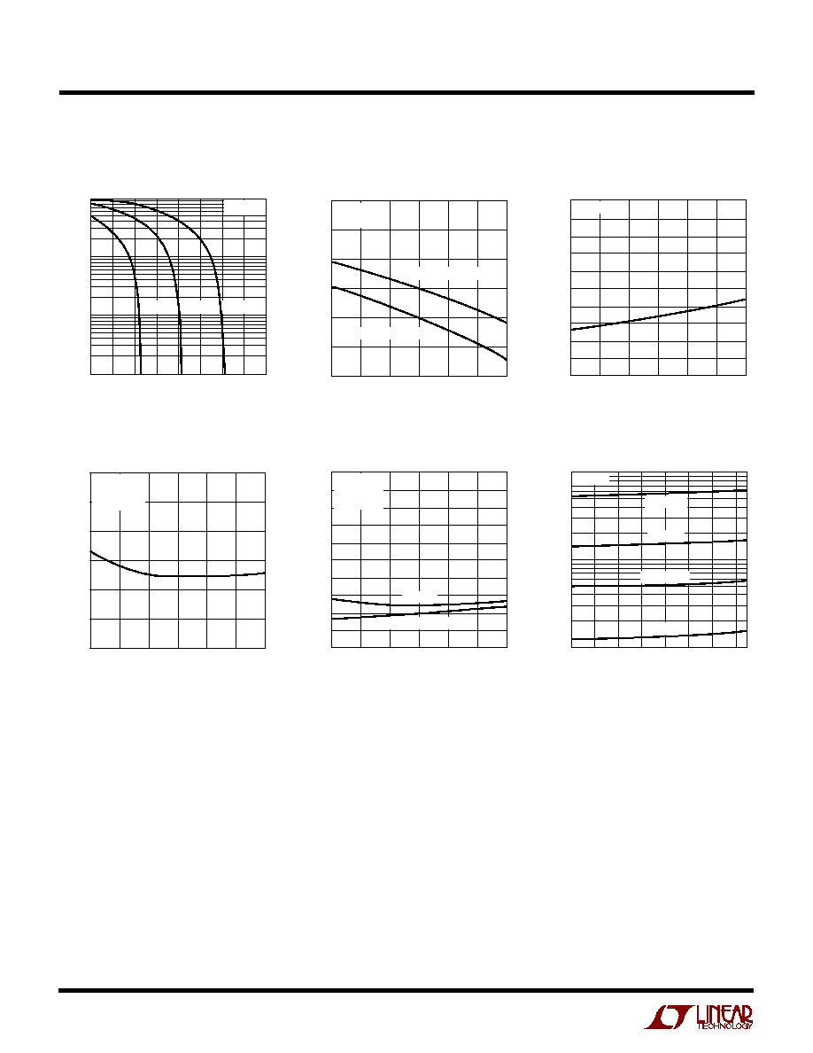
TYPICAL PERFOR A CE CHARACTERISTICS
U
W
MOSFET Gate Drive Current
vs V
GATE
V
+
Fault Threshold Voltage
vs Temperature
Fault Output Low Voltage
vs Temperature
Turn-On Time vs Temperature
Turn-Off Time vs Temperature
Automatic Restart Period
vs Temperature
TEMPERATURE (
°
C)
50
FAULT THRESHOLD VOLTAGE (V) 3.2
3.3
3.4
3.5
3.7
25
0
25
50
1910 G11
75
100
3.6
3.1
V
IN
= 2V
I
F
= 1mA
FAULT HIGH THRESHOLD
FAULT LOW THRESHOLD
TEMPERATURE (
°
C)
50
0
FAULT OUTPUT LOW VOLTAGE (V)
0.04
0.08
0.12
0.10
25
0
25
50
1910 G012
75
0.16
0.20
0.02
0.06
0.14
0.18
100
I
F
= 1mA
TEMPERATURE (
°
C)
50
TURN-ON TIME (
µ
s)
150
200
250
300
400
25
0
25
50
1910 G13
75
100
350
100
V
+
= 24V
V
GATE
= 32V
C
GATE
= 1nF
TEMPERATURE (
°
C)
50
0
TURN-OFF TIME (
µ
s)
20
40
60
50
25
0
25
50
1910 G014
75
80
100
10
30
70
90
100
V
+
= 24V
V
GATE
= 2V
C
GATE
= 1nF
NORMAL
CURRENT LIMIT
TEMPERATURE (
°
C)
30
10
100
1000
10
10
30
50
70
1910 G15
AUTOMATIC RESTART PERIOD (ms)
50
90
V
+
= 24V
C
T
= 3.3
µ
F
C
T
= 0.33
µ
F
C
T
= 0.1
µ
F
C
T
= 1
µ
F
V
GATE
V
+
(V)
0
2
4
MOSFET GATE DRIVE CURRENT (
µ
A)
1
10
100
6
8
10
12
14
16
1910 G10
0.1
V
+
= 8V
V
+
= 12V V
+
24V
T
A
= 25
°
C

5
LT1910
sn1910 1910fs
U
U
U
PI FU CTIO S
GND (Pin 1): Common ground.
TIMER (Pin 2): A timing capacitor C
T
from the TIMER pin
to ground sets the restart time following overcurrent
detection. Upon detection of an overcurrent condition, C
T
is rapidly discharged to less than 1V and then recharged
by a 14
µ
A nominal current source back to the 2.9V timer
threshold, whereupon the restart is attempted. Whenever
TIMER pulls below 2.9V, the GATE pin pulls low to turn off
the external switch. This cycle repeats until the overcur-
rent condition goes away and the switch restarts success-
fully. During normal operation the pin clamps at 3.5V
nominal.
FAULT (Pin 3): The FAULT pin monitors the TIMER pin
voltage and indicates the overcurrent condition. When-
ever the TIMER pin is pulled below 3.3V at the onset of a
current limit condition, the FAULT pin pulls active LOW.
The FAULT pin resets HIGH immediately when the TIMER
pin ramps above 3.4V during autorestart. The FAULT pin
is an open-collector output, thus requiring an external
pull-up resistor and is intended for logic interface. The
resistor should be selected with a typical 1mA pull-up at
low status and less than 2mA under worst-case condi-
tions.
IN (Pin 4): The IN pin threshold is TTL/CMOS compatible
and has approximately 200mV of hysteresis. When the IN
pin is pulled active HIGH above 2V, an internal charge
pump is activated to pull up the GATE pin. The IN pin can
be pulled as high as 15V regardless of whether the supply
is on or off. If the IN pin is left open, an internal 75k pull-
down resistor pulls the pin below 0.8V to ensure that the
GATE pin is inactive LOW.
GATE (Pin 5): The GATE pin drives the power MOSFET
gate. When the IN pin is greater than 2V, the GATE pin is
pumped approximately 12V above the supply. It has
relatively high impedance (the equivalence of a few hun-
dred k
) when pumped above the rail. Care should be
taken to minimize any loading by parasitic resistance to
ground or supply. The GATE pin pulls LOW when the
TIMER pin falls below 2.9V.
SENSE (Pin 6): The SENSE pin connects to the input of a
supply-referenced comparator with a 65mV nominal off-
set. When the SENSE pin is taken more than 65mV below
supply, the MOSFET gate is driven LOW and the timing
capacitor is discharged. The SENSE pin threshold has a
0.33%/
°
C temperature coefficient (TC), which closely
matches the TC of the drain sense resistor formed from the
copper trace of the PCB.
For loads requiring high inrush current, an RC timing delay
can be added between the drain sense resistor and the
SENSE pin to ensure that the current-sense comparator
does not false trigger during start-up (see Applications
Information). A maximum of 10k
can be inserted be-
tween a drain sense resistor and the SENSE pin. If current
sensing is not required, the SENSE pin is tied to supply.
V
+
(Pin 8): In addition to providing the operating current
for the LT1910, the V
+
pin also serves as the Kelvin
connection for the current sense comparator. The V
+
pin
must be connected to the positive side of the drain sense
resistor for proper current sensing operation.