 | ÐлекÑÑоннÑй компоненÑ: LT4254 | СкаÑаÑÑ:  PDF PDF  ZIP ZIP |
Äîêóìåíòàöèÿ è îïèñàíèÿ www.docs.chipfind.ru
LT4254
1
4254f
The LT
®
4254 is a high voltage Hot Swap
TM
controller that
allows a board to be safely inserted and removed from a
live backplane. An internal driver controls the high side
N-channel MOSFET gate for supply voltages ranging from
10.8V to 36V. The part features an open-circuit detect
(OPEN) output that indicates abnormally low load current
conditions.
The LT4254 features an adjustable analog foldback cur-
rent limit. If the supply remains in current limit for more
than a programmable time, the N-channel MOSFET shuts
off, the PWRGD output goes low and the LT4254 either
automatically restarts after a time-out delay or latches off
until the UV pin is cycled low. The RETRY pin sets whether
the part will automatically restart after an overcurrent fault
or if it will latch off until the UV pin is cycled low.
The PWRGD output indicates when the output voltage
rises above a programmed level. An external resistor
string from V
CC
provides programmable undervoltage and
overvoltage protection.
The LT4254 is available in a 16-lead SSOP package.
s
Hot Board Insertion
s
Electronic Circuit Breaker/Power Bussing
s
Industrial High Side Switch/Circuit Breaker
s
24V Industrial/Alarm Systems
s
12V and 24V Distributed Power Systems
, LTC and LT are registered trademarks of Linear Technology Corporation.
s
Allows Safe Board Insertion and Removal from a
Live Backplane
s
Controls Supply Voltage from 10.8V to 36V
s
Foldback Current Limiting
s
Open Circuit and Overcurrent Fault Detect
s
Drives an External N-Channel MOSFET
s
Automatic Retry or Latched Off Operation
After Overcurrent Fault
s
Programmable Supply Voltage Power-Up Rate
s
Undervoltage and Overvoltage Protection
s
Open MOSFET Detection
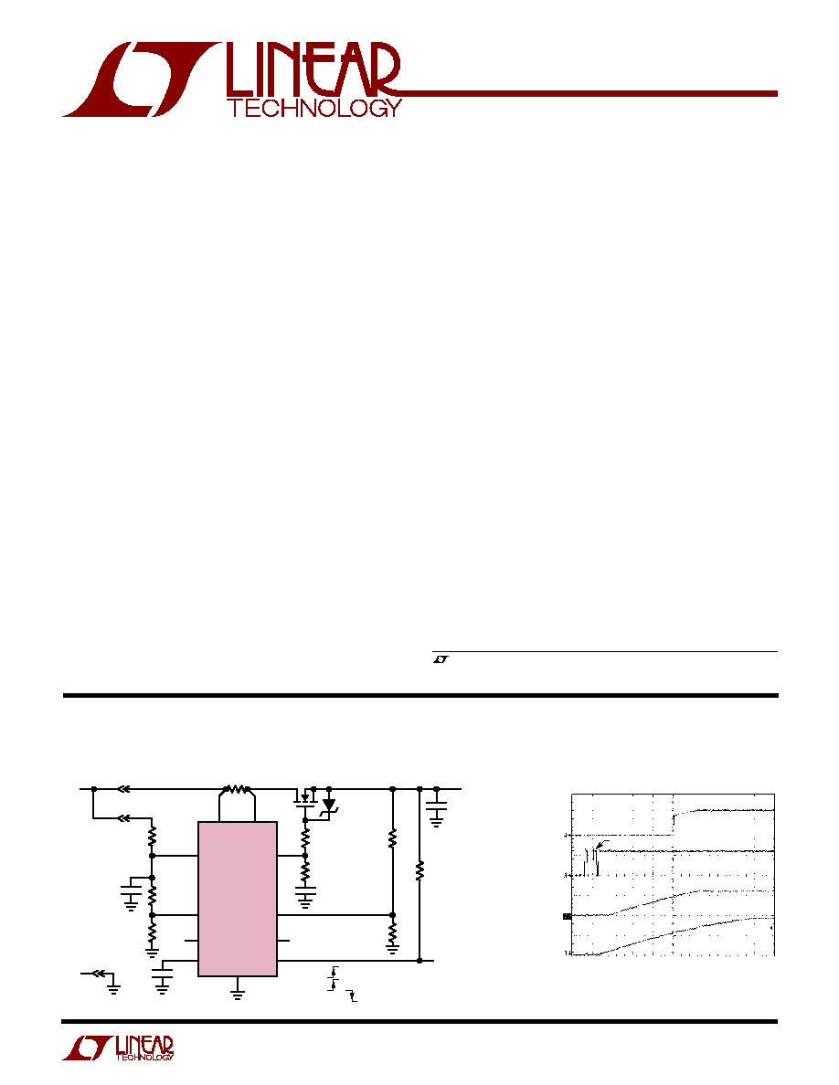
TYPICAL APPLICATIO
U
Positive High Voltage
Hot Swap Controller
with Open-Circuit Detect
Hot Swap is a trademark of Linear Technology Corporation.
4254 TA01
R5
0.025
LT4254
SENSE
13
10
5
7
8
16
15
1
2
4
10
V
CC
GATE
FB
PWRGD
RETRY
UV
OV
TIMER
GND
V
IN
24V
GND
(SHORT PIN)
Q1
IRF530
D1
CMPZ5241B
11V
R3
40.2k
R2
40.2k
R1
324k
R7
100
R9
40.2k
R6
10
R8
140k
PWRGD
V
OUT
24V
1.5A
R4
27k
C
L
C2
33nF
C3
0.1
µ
F
C1
10nF
OPEN
UV = 20V
OV = 40V
PWRGD = 18V
24V, 2A Hot Swap Controller
PWRGD
20V/DIV
V
CC
20V/DIV
V
OUT
20V/DIV
GATE
20V/DIV
2.5ms/DIV
4245 TA02
CONTACT BOUNCE
LT4254 Start-Up Behavior
DESCRIPTIO
U
FEATURES
APPLICATIO S
U
LT4254
2
4254f
Supply Voltage (V
CC
) .................................. 0.3 to 44V
Input Voltage (SENSE, PWRGD) ................. 0.3 to 44V
Input Voltage (GATE) .................................. 0.3 to 50V
Input Voltage (FB, UV, OPEN) ..................... 0.3 to 44V
Input Voltage (OV) ...................................... 0.3 to 18V
Input Voltage (RETRY) ............................... 0.3 to 15V
Minimum Input Voltage (TIMER) ......................... 0.3V
Maximum Input Current (TIMER) ....................... 100
µ
A
Operating Temperature
LT4254C ................................................. 0
°
C to 70
°
C
LT4254I ............................................. 40
°
C to 85
°
C
Storage Temperature Range ................ 65
°
C to 150
°
C
Lead Temperature (Soldering, 10 sec)................. 300
°
C
Consult LTC Marketing for parts specified with wider operating temperature ranges.
ABSOLUTE AXI U
RATI GS
W
W
W
U
PACKAGE/ORDER I FOR ATIO
U
U
W
(Note 1)
ELECTRICAL CHARACTERISTICS
The
q
denotes the specifications which apply over the full operating
temperature range, otherwise specifications are at T
A
= 25
°
C. V
CC
= 24V unless otherwise noted.
SYMBOL
PARAMETER
CONDITIONS
MIN
TYP
MAX
UNITS
V
CC
Operating Voltage
q
10.8
36
V
I
CC
Operating Current
1.9
3
mA
V
UVLH
Undervoltage Threshold
V
CC
Low-to-High Transition
q
3.96
4
4.04
V
V
UVHYS
Hysteresis
0.25
0.4
0.55
V
I
INUV
UV Input Current
UV = 4.5V
0.1
1
µ
A
UV = 0V
1.5
3
µ
A
V
OVHL
Overvoltage Threshold
V
CC
Low-to-High Transition
q
3.96
4
4.04
V
V
OVHYS
Hysteresis
0.25
0.4
0.55
V
I
INOV
OV Input Current
0V
OV < 6.5V
0.1
1
µ
A
V
OPEN
Open-Circuit Voltage Threshold (V
CC
V
SENSE
)
q
2
3.5
5
mV
V
OLOPEN
OPEN Output Low Voltage
I
O
= 2mA
0.20
0.5
V
I
O
= 5mA
0.75
1.3
V
I
INOPEN
Leakage Current
V
OPEN
= 5V
0.1
1
µ
A
V
SENSETRIP
SENSE Pin Trip Voltage (V
CC
V
SENSE
)
FB = 0V
q
5.5
12
25
mV
FB
2V
q
40
50
60
mV
I
INSNS
SENSE Pin Input Current
40
70
µ
A
I
PU
GATE Pull-Up Current
Charge Pump On,
V
GATE
= 7V
q
15
35
55
µ
A
I
PD
GATE Pull-Down Current
Any Fault, V
GATE
= 3V
40
60
80
mA
V
GATE
External N-Channel Gate Drive (Note 2)
V
GATE
V
CC
, 12V
V
CC
20V
q
4.5
8.8
12.5
V
20V
V
CC
36V
q
10
11
12.5
V
V
FB
FB Voltage Threshold
FB High-to-Low Transition
q
3.96
4
4.04
V
FB Low-to-High Transition
q
4.20
4.45
4.65
V
V
FBHYS
FB Hysteresis Voltage
0.3
0.45
0.60
V
V
OLPGD
PWRGD Output Low Voltage
I
O
= 1.6mA
0.25
0.4
V
I
O
= 5mA
0.63
1.0
V
ORDER PART NUMBER
GN PART MARKING
4254
4254I
LT4254CGN
LT4254IGN
1
2
3
4
5
6
7
8
TOP VIEW
GN PACKAGE
16-LEAD PLASTIC SSOP
16
15
14
13
12
11
10
9
UV
OV
NC
OPEN
PWRGD
NC
RETRY
GND
V
CC
SENSE
NC
GATE
NC
NC
FB
TIMER
T
JMAX
= 125
°
C,
JA
= 130
°
C/W
LT4254
3
4254f
I
PWRGD
PWRGD Pin Leakage Current
V
PWRGD
= 36V
0.1
10
µ
A
I
INFB
FB Input Current
FB = 4.5V
1
0.1
µ
A
I
TIMERPU
TIMER Pull-Up Current
q
60
120
180
µ
A
I
TIMERPD
TIMER Pull-Down Current
q
1
3
5
µ
A
D
TIMER
Duty Cycle (RETRY Mode)
q
1.5
3
4.5
%
V
RETRY(TH)
RETRY Threshold
q
0.4
0.8
1.2
V
I
INRTR
RETRY Input Current
RETRY = GND
120
85
40
µ
A
t
PHLUV
UV Low to GATE Low
C
GATE
= 100pF
1.7
µ
s
t
PLHUV
UV High to GATE High
C
GATE
= 100pF
6
µ
s
t
PHLFB
FB Low to PWRGD Low
0.8
µ
s
t
PLHFB
FB High to PWRGD High
3.2
µ
s
t
PHLSENSE
(V
CC
V
SENSE
) High to GATE Low
V
CC
V
SENSE
= 275mV
2.5
4
µ
s
ELECTRICAL CHARACTERISTICS
The
q
denotes the specifications which apply over the full operating
temperature range, otherwise specifications are at T
A
= 25
°
C. V
CC
= 24V unless otherwise noted.
SYMBOL
PARAMETER
CONDITIONS
MIN
TYP
MAX
UNITS
Note 1: Absolute Maximum Ratings are those values beyond which the life
of a device may be impaired.
Note 2: An internal clamp limits the GATE pin to a maximum of 11V above
V
CC
(under normal operating conditions). Driving this pin to a voltage
beyond the clamp voltage may damage the part.
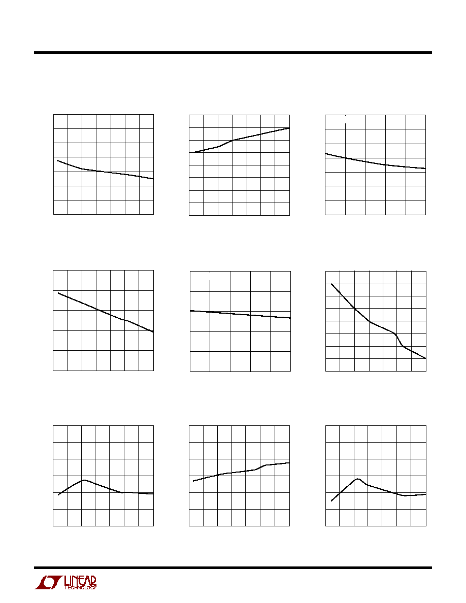
TYPICAL PERFOR A CE CHARACTERISTICS
U
W
I
CC
vs V
CC
SENSE Pin Regulation Voltage
vs Temperature, FB = 0V
SENSE Pin Regulation Voltage
vs Temperature, FB > 2V
TEMPERATURE (
°
C)
50
SENSE REGULATION VOLTAGE (mV)
13
15
17
25
75
4254 G01
11
9
25
0
50
100
125
7
5
TEMPERATURE (
°
C)
50
40
SENSE REGULATION VOLTAGE (mV)
45
50
55
60
25
0
25
50
4254 G02
75
100
125
V
CC
(V)
10.8
I
CC
(mA)
2.0
2.5
30.8
4254 G03
1.5
1.0
15.8
20.8
25.8
36
3.0
T
A
= 25
°
C
LT4254
4
4254f
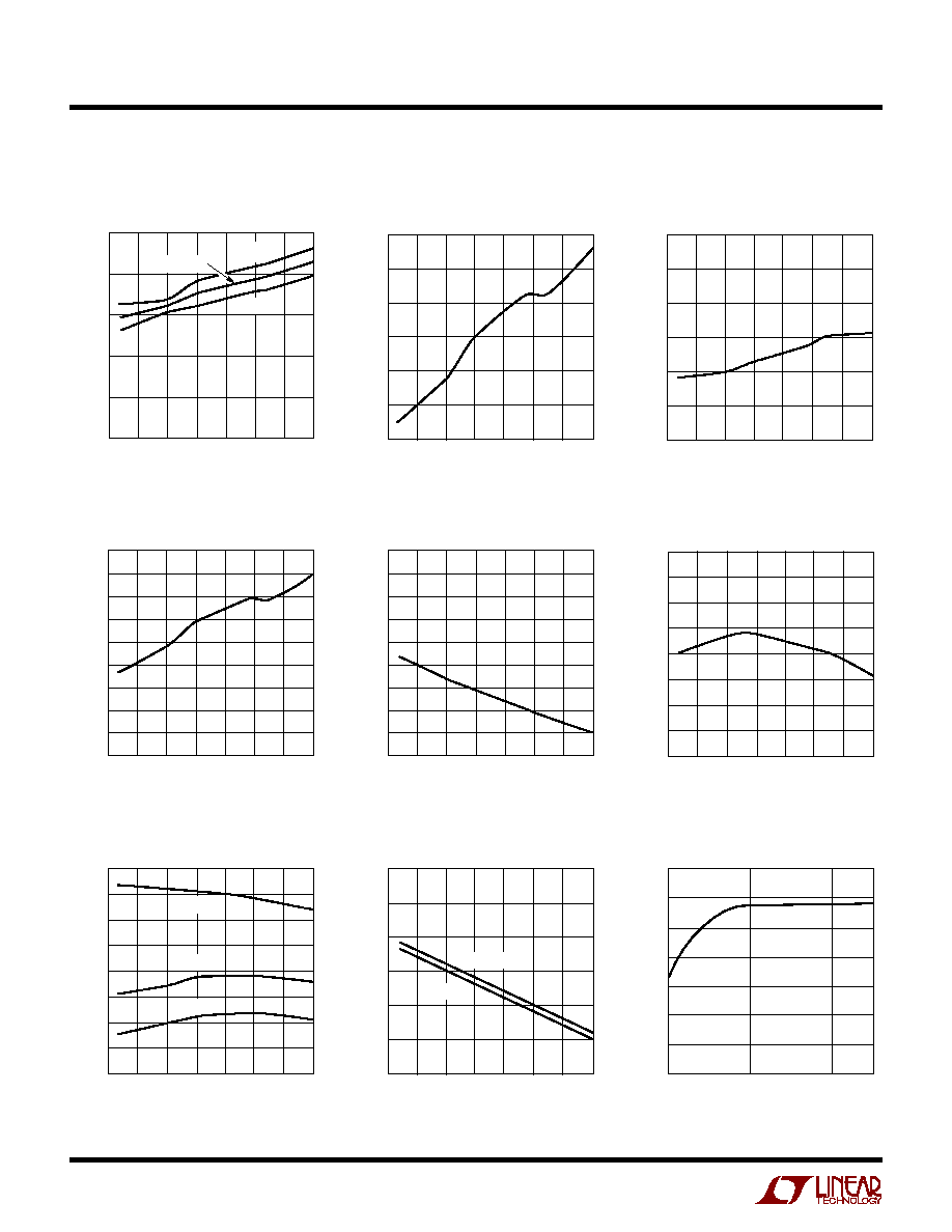
TYPICAL PERFOR A CE CHARACTERISTICS
U
W
FB Pin Hysteresis vs Temperature
GATE Pin Pull-Up Current
vs Temperature
GATE Pin Pull-Down Current
vs Temperature
V
GATE
V
CC
vs Temperature
GATE Drive vs V
CC
I
CC
vs Temperature
FB Pin Threshold Voltage (Low-
to-High) vs Temperature
TEMPERATURE (
°
C)
50
25
1.0
I
CC
(mA)
1.4
2.0
0
50
75
4254 G04
1.2
1.8
1.6
25
100
125
V
CC
= 36V
V
CC
= 10.8V
V
CC
= 24V
TEMPERATURE (
°
C)
50
PWRGD THRESHOLD VOLTAGE LOW-TO-HIGH (V)
4.42
4.44
4.46
25
75
4254 G05
4.40
4.38
25
0
50
100
125
4.36
4.34
TEMPERATURE (
°
C)
50
PWRGD THRESHOLD VOLTAGE HIGH-TO-LOW (V)
4.00
4.01
4.02
25
75
4254 G06
3.99
3.98
25
0
50
100
125
3.97
3.96
FB Pin Threshold Voltage (High-
to-Low) vs Temperature
TEMPERATURE (
°
C)
50
300
PWRGD HYSTERESIS (mV)
320
360
380
400
50
480
4254 G07
340
0
25
75
100
25
125
420
440
460
TEMPERATURE (
°
C)
50
45
I
GATE
PULL-UP CURRENT (
µ
A)
40
30
25
20
50
0
4254 G08
35
0
25
75
100
25
125
15
10
5
TEMPERATURE (
°
C)
50
I
GATE
DOWN (mA)
75
25
4254 G09
60
50
25
0
50
45
40
80
70
65
55
75
100
125
TEMPERATURE (
°
C)
50
V
GATE
V
CC
(V)
11
25
4254 G10
8
6
25
0
50
5
4
12
10
9
7
75
100
125
V
CC
= 18V
V
CC
= 12V
V
CC
= 10.8V
V
GATE
V
CC
vs Temperature
TEMPERATURE (
°
C)
50
V
GATE
V
CC
(V)
12.0
12.5
13.0
25
75
4254 G11
11.5
11.0
25
0
50
100
125
10.5
10.0
V
CC
= 24V, 36V
V
CC
= 20V
V
CC
(V)
10.8
10
12
14
T
A
= 25
°
C
30.8
36
4254 G12
8
6
20.8
4
2
0
GATE DRIVE (V
GATE
V
CC
) (V)
LT4254
5
4254f
TYPICAL PERFOR A CE CHARACTERISTICS
U
W
Timer Shutdown Threshold
vs Temperature
I
TIMER
Up vs V
CC
UV Threshold Voltage (High-to-
Low) vs Temperature
TIMER Pin Pull-Up Current
vs Temperature
UV Hysteresis vs Temperature
TEMPERATURE (
°
C)
50
25
145
125
135
TIMER PULL-UP CURRENT (
µ
A)
105
75
0
50
75
4254 G13
115
85
95
25
100
125
TIMER Pin Pull-Down Current
vs Temperature
TEMPERATURE (
°
C)
50
TIMER PULL-DOWN CURRENT (
µ
A)
3.5
25
4254 G14
2.0
1.0
25
0
50
0.5
0
4.0
3.0
2.5
1.5
75
100
125
TIMER Pin Pull-Down Current
vs V
CC
V
CC
(V)
10.8
3.0
3.2
3.4
30.8
4254 G15
2.8
2.6
15.8
20.8
25.8
36
2.4
2.2
2.0
I
TIMER
DOWN (
µ
A)
T
A
= 25
°
C
TEMPERATURE (
°
C)
50
25
4.0
TIMER SHUTDOWN THRESHOLD VOLTAGE (V)
4.4
5.0
0
50
75
4254 G16
4.2
4.8
4.6
25
100
125
V
CC
(V)
10.8
I
TIMER
UP (
µ
A)
114
112
110
30.8
4254 G17
116
118
120
15.8
20.8
25.8
36
T
A
= 25
°
C
TEMPERATURE (
°
C)
50
UV THRESHOLD VOLTAGE HIGH-TO-LOW (V)
3.65
25
4254 G18
3.62
3.60
25
0
50
3.59
3.58
3.66
3.64
3.63
3.61
75
100
125
UV Threshold Voltage (Low-to-
High) vs Temperature
TEMPERATURE (
°
C)
50
UV THRESHOLD VOLTAGE LOW-TO-HIGH (V)
4.00
4.01
4.02
25
75
4254 G19
3.99
3.98
25
0
50
100
125
3.97
3.96
TEMPERATURE (
°
C)
50
UV HYSTERESIS (mV)
400
450
500
25
75
4254 G20
350
300
25
0
50
100
125
250
200
OV Threshold Voltage (Low-to-
High) vs Temperature
TEMPERATURE (
°
C)
50
OV THRESHOLD VOLTAGE (LOW-TO-HIGH) (V)
4.00
4.01
4.02
25
75
4257 G21
3.99
3.98
25
0
50
100
125
3.97
3.96