 | –≠–ª–µ–∫—Ç—Ä–æ–Ω–Ω—ã–π –∫–æ–º–ø–æ–Ω–µ–Ω—Ç: LT5500 | –°–∫–∞—á–∞—Ç—å:  PDF PDF  ZIP ZIP |
1
LT5500
5500i
1.8GHz to 2.7GHz
Receiver Front End
December 2001
FEATURES
DESCRIPTIO
N
U
s
1.8V to 5.25V Supply
s
Dual LNA Gain Setting: +13.5dB/≠14dB at 2.5GHz
s
Double-Balanced Mixer
s
Internal LO Buffer
s
LNA Input Internally Matched
s
Low Supply Current: 23mA
s
Low Shutdown Current: 2
µ
A
s
24-Lead Narrow SSOP Package
The LT
Æ
5500 is a receiver front end IC designed for low
voltage operation and is compatible with the LTC family of
WLAN products. The chip contains a low noise amplifier
(LNA), a Mixer and an LO buffer. The IC is designed to
operate over a power supply voltage range from 1.8V to
5.25V.
The LNA can be set to either high gain or low gain mode.
At 2.5GHz, the high gain mode provides 13.5dB gain and
a noise figure (NF) of 4dB. The LNA in low gain mode
provides ≠14dB gain and an IIP3 of + 8dBm at 2.5GHz.
The mixer has 5dB of conversion gain and an IIP3 of
≠ 2.5dBm at 2.5GHz, with ≠10dBm LO input power.
APPLICATIO
N
S
U
s
IEEE 802.11 and 802.11b DSSS and FHSS
s
High Speed Wireless LAN
s
Wireless Local Loop
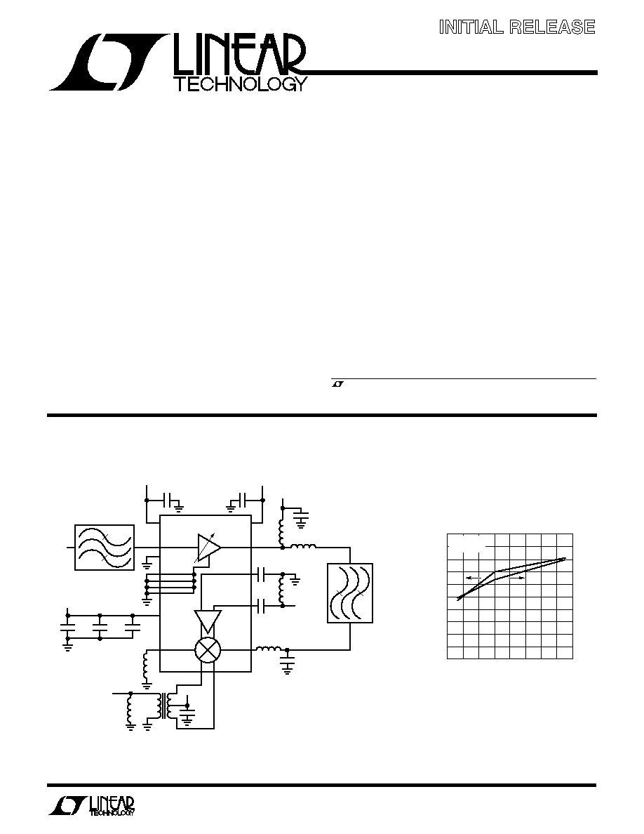
Figure 1. 2.5GHz Receiver. Interstage Filter is Optional
TYPICAL APPLICATIO
N
U
, LTC and LT are registered trademarks of Linear Technology Corporation.
LO
MIX_IN
LO
+
LO
≠
LNA_OUT
LNA_IN
LNA_GND
GND
GS
EN
LT5500
MIX_GND
V
CC
2V
IF
≠
5500 F01
IF
+
2V
∑
∑
T2
8:1
IF
RF
C4
C17
C23
L3
L5
L7
IF OUTPUT
RF
INPUT
L4
100pF
◊
2
L2
2V
GAIN
SELECT
BAND SELECT
FILTER
ENABLE
100pF
100pF
L9
LO INPUT
INTERSTAGE
FILTER
100pF
◊
4
1nF
100pF
1
µ
F
LNA Gain (High Gain Mode)
and Mixer Conversion Gain
Information furnished by Linear Technology Corporation is believed to be accurate and reliable.
However, no responsibility is assumed for its use. Linear Technology Corporation makes no represen-
tation that the interconnection of its circuits as described herein will not infringe on existing patent rights.
Final Electrical Specifications
V
CC
(V)
1.5
LNA GAIN (dB)
MIXER CONVERSION GAIN (dB)
13.4
13.6
13.7
5.5
5500 TA02
13.2
13.0
2.5
3.5
4.5
2
3
4
5
14.0
13.3
13.5
13.1
13.8
13.9
4.8
5.2
5.4
4.4
4.0
6.0
4.6
5.0
4.2
5.6
5.8
f
RF
= 2.5GHz
T
A
= 25
∞
C

2
LT5500
5500i
W
U
U
PACKAGE/ORDER I FOR ATIO
LT5500EGN
T
JMAX
= 150
∞
C,
JA
= 85
∞
C/W
ORDER PART
NUMBER
ABSOLUTE
M
AXI
M
U
M
RATINGS
W
W
W
U
(Note 1)
Power Supply Voltage ........................................... 5.5V
LNA RF Input Power ............................................ 5dBm
Mixer RF Input Power ........................................ 10dBm
LO Input Power (Note 2) ................................... 10dBm
All Other Pins ......................................................... 5.5V
Operating Ambient
Temperature Range ............................... ≠ 40
∞
C to 85
∞
C
Storage Temperature Range ................ ≠ 65
∞
C to 150
∞
C
Lead Temperature (Soldering, 10 sec)................. 300
∞
C
(Test circuit shown in Figure 3 for 1.8GHz application) V
CC
= 3V DC,
LNA: f
LNA_IN
= 1.8GHz, Mixer: f
MIX_IN
= 1.8GHz, f
LO
= 1.52GHz, P
LO
= ≠10dBm, T
A
= 25
∞
C, unless otherwise noted. (Notes 3, 4)
1
2
3
4
5
6
7
8
9
10
11
12
TOP VIEW
GN PACKAGE
24-LEAD PLASTIC SSOP
24
23
22
21
20
19
18
17
16
15
14
13
EN
V
CC
LNA_IN
GND
LNA_GND
LNA_GND
LNA_GND
LNA_GND
V
CC
MIX_GND
GND
IF
+
GS
GND
LNA_OUT
V
CC
GND
LO
≠
LO
+
V
CC
GND
MIX_IN
GND
IF
≠
Consult LTC Marketing for parts specified with wider operating temperature ranges.
ELECTRICAL CHARACTERISTICS
SYMBOL
PARAMETER
CONDITIONS
MIN
TYP
MAX
UNITS
LNA High Gain: EN = 1.35V, GS = 1.35V
Frequency Range (Note 3)
1.8 to 2.7
GHz
Forward Gain
15.5
18.5
dB
Reverse Gain (Isolation)
≠39
dB
Noise Figure
Terminated 50
Source
2.5
dB
Input Return Loss
No External Matching
10.5
dB
Output Return Loss
With External Matching
15
dB
Input 1dB Compression
≠24
dBm
Input 3rd Order Intercept
Two Tone Test,
f = 2MHz
≠18
≠12
dBm
LNA Low Gain: EN = 1.35V, GS = 0.3V
Frequency Range (Note 4)
1.8 to 2.7
GHz
Forward Gain
≠13
≠10
dB
Reverse Gain (Isolation)
≠34
dB
Noise Figure
16.5
dB
Input 1dB Compression
0
dBm
Input 3rd Order Intercept
Two Tone Test,
f = 2MHz
4.5
9
dBm
Mixer: EN = 1.35V, GS = 1.35V
RF Frequency Range (Note 4)
1.8 to 2.7
GHz
Conversion Gain
5.5
8.5
dB
SSB Noise Figure
Terminated 50
Source
7.5
dB
Input P1dB
≠13
dBm
Input 3rd Order Intercept
Two Tone Test,
f = 2MHz
≠6
≠ 2.5
dBm
3
LT5500
5500i
(Test circuit shown in Figure 3 for 1.8GHz application) V
CC
= 3V DC,
LNA: f
LNA_IN
= 1.8GHz, Mixer: f
MIX_IN
= 1.8GHz, f
LO
= 1.52GHz, P
LO
= ≠10dBm, T
A
= 25
∞
C, unless otherwise noted. (Notes 3, 4)
ELECTRICAL CHARACTERISTICS
(Test circuit shown in Figure 3 for 2.5GHz application) V
CC
= 3V DC, LNA: f
LNA_IN
= 2.5GHz, Mixer: f
MIX_IN
= 2.5GHz, f
LO
= 2.22GHz,
P
LO
= ≠10dBm, T
A
= 25
∞
C, unless otherwise noted.
SYMBOL
PARAMETER
CONDITIONS
MIN
TYP
MAX
UNITS
LO Frequency Range (Note 4)
1.35 to 3.15
GHz
IF Frequency Range (Note 3)
200 to 450
MHz
LO-IF Isolation
36
dB
LO-RF Isolation
36
dB
RF-LO Isolation
40
dB
SYMBOL
PARAMETER
CONDITIONS
MIN
TYP
MAX
UNITS
LNA High Gain: EN = 1.35V, GS = 1.35V
Forward Gain
13.5
dB
Reverse Gain (Isolation)
≠35
dB
Noise Figure
Terminated 50
Source
4
dB
Input Return Loss
No External Matching
12
dB
Output Return Loss
With External Matching
15
dB
Input 1dB Compression
≠15
dBm
Input 3rd Order Intercept
Two Tone Test,
f = 2MHz
≠3.5
dBm
LNA Low Gain: EN = 1.35V, GS = 0.3V
Forward Gain
≠14
dB
Reverse Gain (Isolation)
≠39
dB
Noise Figure
19
dB
Input 1dB Compression
≠1
dBm
Input 3rd Order Intercept
Two Tone Test,
f = 2MHz
8
dBm
Mixer: EN = 1.35V, GS = 1.35V
Conversion Gain
5
dB
SSB Noise Figure
Terminated 50
Source
9.5
dB
Input P1dB
≠11
dBm
Input 3rd Order Intercept
Two Tone Test,
f = 2MHz
≠ 2.5
dBm
LO-IF Isolation
33
dB
LO-RF Isolation
37
dB
RF-LO Isolation
32
dB
V
CC
= 3V DC, T
A
= 25
∞
C (Note 4)
Note 1: Absolute Maximum Ratings are those values beyond which the life of
the device may be impaired.
Note 2: LO Absolute Maximum Ratings apply for each LO pin separately.
Note 3: Component values listed in Figure 3 for 1.8GHz evaluation board were
used to guarantee 1.8GHz performance.
Note 4: Specifications over the ≠40
∞
C to 85
∞
C operating temperature range
are assured by design, characterization and correlation with statistical process
controls.
Note 5: When EN
0.3V, enable current is <10
µ
A.
Note 6: When GS
0.3V, gain select current is <10
µ
A.
SYMBOL
PARAMETER
CONDITIONS
MIN
TYP
MAX
UNITS
Power Supply
V
CC
Supply Voltage
1.8 to 5.25
V
I
CC
HG
Rx High Gain Mode
EN = 1.35V, GS = 1.35V
23
33
mA
I
CC
LG
Rx Low Gain Mode
EN = 1.35V, GS = 0.3V
18
31
mA
I
CC
Off
Shutdown Current
EN = 0.3V, GS = 0.3V
2
25
µ
A
I
EN
Enable Current
EN = 1.35V (Note 5)
21
µ
A
I
GS
Gain Select Current
GS = 1.35V (Note 6)
21
µ
A

4
LT5500
5500i
TYPICAL PERFOR A CE CHARACTERISTICS
U
W
LNA IIP3 vs Supply Voltage and
Temperature (High Gain Mode)
LNA Noise Figure vs Supply
Voltage (High Gain Mode)
LNA IIP3 vs Supply Voltage and
Temperature (Low Gain Mode)
LNA Noise Figure vs Supply
Voltage (Low Gain Mode)
LNA Gain vs Supply Voltage and
Temperature (High Gain Mode)
SUPPLY VOLTAGE (V)
1.5
GAIN (dB)
16
18
5.5
5500 G01
14
12
2.5
3.5
4.5
2
3
4
5
20
15
17
13
19
≠40
∞
C, 1.8GHz
≠40
∞
C, 2.5GHz
25
∞
C, 1.8GHz
85
∞
C, 1.8GHz
85
∞
C, 2.5GHz
25
∞
C, 2.5GHz
SUPPLY VOLTAGE (V)
1.5
≠20
IIP3 (dBm)
≠18
≠14
≠12
≠10
0
≠6
2.5
3.5
4
5500 G02
≠16
≠4
≠2
≠8
2
3
4.5
5
5.5
≠40
∞
C, 1.8GHz
≠40
∞
C, 2.5GHz
25
∞
C, 1.8GHz
85
∞
C, 1.8GHz
85
∞
C, 2.5GHz
25
∞
C, 2.5GHz
SUPPLY VOLTAGE (V)
1.5
NOISE FIGURE (dB)
3.5
4.0
4.5
3
4
5.5
5500 G03
3.0
2.5
2.0
2
2.5
3.5
4.5
5
2.5GHz
T
A
= 25
∞
C
1.8GHz
LNA Gain vs Supply Voltage and
Temperature (Low Gain Mode)
SUPPLY VOLTAGE (V)
1.5
GAIN (dB)
≠12.0
≠11.5
≠11.0
5.5
5500 G04
≠12.5
≠13.0
≠14.5
≠14.0
2
2.5
3
3.5
4
4.5
5
≠13.5
≠10.0
≠10.5
≠40
∞
C, 1.8GHz
≠40
∞
C, 2.5GHz
25
∞
C, 1.8GHz
25
∞
C, 2.5GHz
85
∞
C, 1.8GHz
85
∞
C, 2.5GHz
SUPPLY VOLTAGE (V)
1.5
IIP3 (dBm)
4
6
8
2.5
3.5
4.5
5.5
5500 G05
10
12
2
3
4
5
≠40
∞
C, 1.8GHz
≠40
∞
C, 2.5GHz
25
∞
C, 2.5GHz
85
∞
C, 1.8GHz
85
∞
C, 2.5GHz
25
∞
C, 1.8GHz
SUPPLY VOLTAGE (V)
1.5
18.0
18.5
19.5
4.5
5500 G06
17.5
17.0
2.5
3.5
5.5
16.5
16.0
19.0
NOISE FIGURE (dB)
2.5GHz
1.8GHz
T
A
= 25
∞
C
Mixer Conversion Gain vs Supply
Voltage and Temperature
Mixer IIP3 vs Supply Voltage and
Temperature
Mixer SSB Noise Figure
vs Supply Voltage
SUPPLY VOLTAGE (V)
1.5
4
CONVERSION GAIN (dB)
5
6
7
8
2.5
3.5
4.5
5.5
5500 G07
9
10
2
3
4
5
≠40
∞
C, 1.8GHz
≠40
∞
C, 2.5GHz
85
∞
C, 1.8GHz
25
∞
C, 1.8GHz
85
∞
C, 2.5GHz
25
∞
C, 2.5GHz
SUPPLY VOLTAGE (V)
1.5
IIP3 (dBM)
≠2
0
5.5
5500 G08
≠4
≠6
2.5
3.5
4.5
2
3
4
5
2
≠3
≠1
≠5
1
≠40
∞
C, 1.8GHz
≠40
∞
C, 2.5GHz
25
∞
C, 1.8GHz
85
∞
C, 1.8GHz
85
∞
C, 2.5GHz
25
∞
C, 2.5GHz
SUPPLY VOLTAGE (V)
1.5
7.0
NOISE FIGURE (dB)
7.5
8.0
8.5
9.0
2.5
3.5
4.5
5.5
5500 G09
9.5
10.0
2
3
4
5
2.5GHz
1.8GHz
T
A
= 25
∞
C

5
LT5500
5500i
TYPICAL PERFOR A CE CHARACTERISTICS
U
W
Mixer Conversion Gain
vs LO Power
Mixer IIP3 vs LO Power
P(LO) (dBm)
0
0
CONVERSION GAIN (dB)
1
3
4
5
≠20
9
5500 G10
2
≠10
≠5
≠25
≠15
≠30
6
7
8
2.5GHz
1.8GHz
IF = 280MHz
V
CC
= 3V
T
A
= 25
∞
C
LNA Input Return Loss
vs Supply Voltage
Mixer SSB Noise Figure
vs LO Power
P(LO) (dBm)
0
CONVERSION GAIN (dB)
10
11
12
≠15
≠25
5500 G11
9
8
7
≠5
≠10
≠20
13
14
15
≠30
2.5GHz
1.8GHz
IF = 280MHz
V
CC
= 3V
T
A
= 25
∞
C
P(LO) (dBm)
0
≠3.0
IIP3 (dBm)
≠2.6
≠2.2
≠1.8
≠5
≠10
≠15
≠20
5500 G12
≠25
≠1.4
≠1.0
≠2.8
≠2.4
≠2.0
≠1.6
≠1.2
≠30
2.5GHz
1.8GHz
IF = 280MHz
V
CC
= 3V
T
A
= 25
∞
C
LNA Input Return Loss
vs Temperature
LNA Output Return Loss
vs Supply Voltage
V
CC
(V)
1.5
RL1 (dB)
11
12
13
5.5
5500 G13
10
9
6
7
2.5
3.5
4.5
8
15
14
LOW GAIN
HIGH GAIN
RF = 2.5GHz
T
A
= 25
∞
C
TEMPERATURE (
∞
C)
≠50
6
RL1 (dB)
8
10
12
14
18
0
50
HIGH GAIN
LOW GAIN
5500 G14
100
16
RF = 2.5GHz
V
CC
= 3V
V
CC
(V)
1.5
RL2 (dB)
16
18
20
5.5
5500 G15
14
12
6
8
2.5
3.5
4.5
10
24
22
LOW GAIN
HIGH GAIN
RF = 2.5GHz
T
A
= 25
∞
C
LNA Output Return Loss
vs Temperature
I
VCC
vs Supply Voltage
(High Gain Mode)
I
VCC
vs Supply Voltage
(Low Gain Mode)
TEMPERATURE (
∞
C)
≠50
20
18
16
14
12
10
8
6
5500 G16
0
50
HIGH GAIN
100
RL2 (dB)
LOW GAIN
RF = 2.5GHz
V
CC
= 3V
V
CC
(V)
1.5
I
VCC
(mA)
23
25
27
5.5
5500 G17
21
19
15
2.5
3.5
4.5
17
31
85
∞
C
25
∞
C
≠40
∞
C
29
V
CC
(V)
1.5
I
VCC
(mA)
20
22
24
5.5
5500 G18
18
16
12
2.5
3.5
4.5
14
28
85
∞
C
25
∞
C
≠40
∞
C
26

6
LT5500
5500i
PI
N
FU
N
CTIO
N
S
U
U
U
EN (Pin 1): Enable Pin. A voltage less than 0.3V (Logic Low)
disables the part. An input greater than 1.35V (Logic High)
enables the part. This pin should be bypassed to ground with
a 100pF capacitor. To shut down the part, this pin and GS
(Pin 24) must be logic low. Voltage on this pin should not
exceed V
CC
nor fall below ground.
V
CC
(Pins 2, 9, 17, 21): Power Supply Pins. See Figure 6
for recommended power supply bypassing.
LNA_IN (Pin 3): LNA Input Pin. The LT5500 has better
than 10dB input return loss from 1.8GHz to 2.7GHz. This
pin is internally biased to 0.8V and must be AC coupled.
GND (Pin 4, 11, 14, 16, 20, 23): Ground Pins. These pins
should be connected directly to ground.
LNA_GND (Pins 5, 6, 7, 8): LNA Ground Pins. These pins
control the gain of the LNA. At higher frequencies, these
pins must be connected directly to ground to maximize the
gain.
MIX_GND (Pin 10): Mixer Ground Pin. To optimize the
performance of the mixer, a 4.7nH inductor to ground is
required for this pin.
IF
+
, IF
≠
(Pins 12, 13): Intermediate Frequency (IF) Mixer
Output Pins. These pins must be inductively tied to V
CC
.
The output can be taken differentially or transformed into
a single ended output, depending on user preference and
performance requirements.
MIX_IN (Pin 15): Mixer RF Input. This pin is internally
biased to 0.83V and must be AC coupled. An external
matching network is necessary to match to a 50
system.
LO
+
, LO
≠
(Pins 18, 19): LO Input Pins. These pins are
used to provide the LO drive to the mixer. The signal can
be provided either single ended or differentially. These
pins are internally biased to V
CC
≠ 0.2V and must be AC
coupled.
LNA_OUT (Pin 22): The Output Pin for the LNA. An
external matching network is necessary to match to a 50
system. This pin must be DC coupled to the power supply.
GS (Pin 24): Gain Select Pin. This pin is used to select
between high gain and low gain modes. High gain mode is
selected when an input voltage greater than 1.35V (Logic
High) is applied to this pin. Low gain mode is selected
when the applied voltage is less than 0.3V (Logic Low).
This pin should be bypassed to ground with a 100pF
capacitor. To shut down the part, this pin must be logic
low. Voltage on this pin should not exceed V
CC
nor fall
below ground.

7
LT5500
5500i
BLOCK DIAGRA
W
Figure 2. LT5500 Block Diagram
LO
MIX_IN
LO
+
LO
≠
LNA_OUT
LNA_IN
LNA_GND
GND
GS
EN
1
3
5
6
7
8
2, 9, 17, 21
10
12
13
5500 BD
15
18
19
22
24
4, 11, 14, 16, 20, 23
LT5500
MIX_GND
V
CC
IF
≠
IF
+
IF
RF
BIAS
APPLICATIO
N
S I
N
FOR
M
ATIO
N
W
U
U
U
The LT5500 consists of an LNA, a Mixer, an LO buffer and
the associated bias circuitry. The chip is designed to be
compatible with IEEE802.11b wireless local area network
(WLAN), MMDS and other wireless applications. The LNA
and Mixer are designed to operate over an input frequency
range of 1.8GHz to 2.7GHz with a supply voltage of 1.8V
to 5.25V. The Mixer IF output frequency range is 200MHz
to 450MHz. The typical LO drive is ≠10dBm. The LO buffer
operation is broadband.
LNA
The LNA has two modes of operation: high gain and low
gain. In the high gain mode, the LNA is a cascode
amplifier. Package inductance is used to achieve better
than 10dB input return loss over the entire frequency
range. The input of the LNA must be AC coupled. The
linearity of the high gain mode of the LNA can be in-
creased by adding inductance to LNA_GND. This will
reduce the gain and improve input return loss while
having little impact on the low gain mode. In low gain
mode, the LNA uses a capacitively coupled diode and a
resistively degenerated cascode to attenuate the incom-
ing signal and maintain a moderate VSWR. The LNA
output is an open collector, and the matching circuit
requires a shunt inductor connected to the power supply
to provide the bias current. The component configuration
for matching and example component values are listed in
Figure 3. If it is desirable to reduce the gain further and
simultaneously broaden the LNA bandwidth, an addi-
tional shunt resistor to the power supply can be added to
the output to reduce the output quality factor (Q).
The LT5500 is designed to allow an interstage bandpass
filter to be introduced between the output of the LNA and
the input of the Mixer. If such an interstage filter is
unnecessary, the output of the LNA can be connected to
the Mixer input through a blocking capacitor and small
value resistor.
Mixer
The Mixer consists of a single-ended input differential pair
followed by a double-balanced mixer cell. The input match-
ing configuration for the Mixer is shown in Figure 3. The
Mixer uses a 4.7nH external inductance to act as a high
frequency current source at the MIX_GND pin. Example
component values for matching the mixer input are tabu-
lated in Figure 3.

8
LT5500
5500i
APPLICATIO
N
S I
N
FOR
M
ATIO
N
W
U
U
U
LO
MIX_IN
LO
+
LO
≠
LNA_OUT
LNA_IN
RF OUT
LNA_GND
GND
GS
EN
LT5500
MIX_GND
V
CC
*REFER TO FIGURE 6 FOR POWER SUPPLY
PINS BYPASSING RECOMMENDATION
V
CC
IF
≠
5500 F03
IF
+
V
CC
∑
∑
T1
IF
RF
C4
100pF
100pF
C17
L3
L5
4.7nH
L7
IF OUTPUT
RF INPUT
L4
100pF
100pF
L2
GAIN
SELECT
ENABLE
LO INPUT
MIXER RF
INPUT
C2
100pF
APPLICATION DEPENDENT
COMPONENT VALUES
RF INPUT
L4
L2
L3
C4
C17
L9
C23
L7
T1
1.8GHz
4.7nH
12nH
4.7nH
220pF
10pF
5.6nH
1.8pF
280MHz IF OUTPUT
2.5GHz
2.7nH
4.7nH
1.8nH
220pF
10pF
2.7nH
1.5pF
BIAS
C23
L9
V
CC
15nH
TC8-1 MINI-CIRCUITS
*
Figure 3. Simplified Test Schematic for 1.8GHz and 2.5GHz Applications
An IF transformer can be used to create a single-ended
output. The additional discrete components necessary to
achieve a 50
match are tabulated in Figure 3. Alterna-
tively, the discrete solution shown in Figure 4 can be used
to perform differential to single-ended conversion. For
best LO and RF signal suppression at the IF output, a
transformer should be used. If it is desirable to reduce the
gain of the mixer, a resistor between the IF outputs can be
used.
LO Buffer
The LO inputs can be driven either differentially or single
ended. A single-ended configuration is shown along with
example component values in Figure 3. Optionally, the LO
can be driven differentially as shown in Figure 5.
C14
C12
L10
V
CC
L11
100pF
5500 F04
13
12
50
IF OUTPUT
LT5500
IF
+
IF
≠
IF OUTPUT
L10, L11
C12
C14
280MHz
27nH
3.3pF
2.2pF
Figure 4. Alternative Mixer IF Output Matching
Figure 5. Optional Transformer-Based Differential LO Drive
L3
5500 F05
TX1
4:1
LO INPUT
L3
TX1
2.22GHz
3.3
µ
H
TOKO-BF4
LO INPUT
19
18
LT5500
LO
≠
LO
+
9
LT5500
5500i
APPLICATIO
N
S I
N
FOR
M
ATIO
N
W
U
U
U
Modes of Operation
The LT5500 has three operating modes:
1. Shutdown
2. LNA High Gain
3. LNA Low Gain
For shutdown, the EN pin and the GS pin must be at logic
Low. Logic Low is defined as a control voltage below 0.3V.
LNA High gain mode requires that both EN and GS pins be
at logic High. Logic High is defined as a control voltage
above 1.35V. LNA Low gain mode requires that the EN pin
be at logic High and that the GS pin be at logic Low. Mixer
operation is independent of the GS pin. The Mixer is
enabled when the EN pin is at logic High.
Table 1: Mode Selection
EN
GS
LNA
MIXER
High
High
High Gain
On
High
Low
Low Gain
On
Low
Low
Shutdown
Shutdown
Evaluation Board
Figure 6 shows the circuit schematic of the evaluation
board. Each signal terminal of the evaluation board has
provisions for three matching components in a T-forma-
tion. In practice, two or fewer components are needed to
achieve the match. In the case of the LNA input, no external
components are necessary if the band select filter pro-
vides the necessary AC coupling. Otherwise AC coupling
must be provided. A similar consideration applies to the
Mixer input pin. The LO terminal of the evaluation board
was designed to permit evaluation of both single ended
and differential matching configurations. The differential
configuration anticipates the use of a transformer. Simi-
larly, the IF output board layout was designed to permit
evaluation of both transformer based and discrete compo-
nent based matching.
The evaluation board employs primarily 0402 surface
mount components, particularly near the signal paths. All
surface mount inductors must have a high self-resonance
frequency. The component values necessary for 1.8GHz
and 2.5GHz applications are tabulated in Figure 3.
RF Layout Tips
∑ Use 50
impedance transmission lines up to the match-
ing networks. Use of ground planes is a must, particu-
larly beneath the IC.
∑ Keep the matching networks as close to the pins as
possible.
∑ Surface mount 0402 outline (or smaller) parts are
recommended to minimize parasitic capacitances and
inductances.
∑ Improve LO isolation and maximize component density
by putting the LO signal trace on the bottom of the
board. This permits either the matching components or
an interstage filter to be placed directly between the
LNA output and the Mixer input.
∑ Place bypass capacitors to ground in close proximity to
the pull-up inductors on the LNA and Mixer outputs to
improve component behavior and assure a good small-
signal ground.
∑ V
CC
lines must be decoupled with low impedance,
broadband capacitors to prevent instability. The capaci-
tors should be placed as close as possible to the V
CC
pins.
∑ Avoid use of long traces whenever possible. Long RF
traces in particular lead to signal radiation, degraded
isolation and higher losses.

10
LT5500
5500i
APPLICATIO
N
S I
N
FOR
M
ATIO
N
W
U
U
U
GS
GND
LNA_OUT
V
CC
GND
LO
≠
LO
+
V
CC
GND
MIX_IN
GND
IF
≠
EN
V
CC
LNA_IN
GND
LNA_GND
LNA_GND
LNA_GND
LNA_GND
V
CC
MIX_GND
GND
IF
+
24
23
22
21
20
19
18
17
16
15
14
13
1
2
3
4
5
6
7
8
9
10
11
12
LT5500
C3
100pF
C2
1
µ
F
J2
LNA_IN
C25
100pF
C24
100pF
C6
1
µ
F
C4 220pF
C8 1
µ
F
C17
10pF
C22
100pF
L4
2.7nH
L3
1.8nH
L2
4.7nH
C5 100pF
C10 100pF
C9
100pF
C13
1nF
L5
4.7nH
E2
V
CC1
V
CC2
E1
V
CC1
V
CC1
R4 0
R3 0
R1
5.1k
SW1
4
3
1
2
R2
5.1k
C1
100pF
C16
8.2pF
R6
0
C28
1.5pF
L6
2.7nH
J1
LNA_OUT
J3
LO_IN
J5
MIX_IN
J6
IF_OUT
E4
E5
5500 F06
C15
100pF
T1
3
2
1
4
6
∑
∑
L7
15nH
R5
0
Figure 6. 2.5GHz Evaluation Circuit Schematic

11
LT5500
5500i
APPLICATIO
N
S I
N
FOR
M
ATIO
N
W
U
U
U
Figure 7. Component Side Silkscreen of Evaluation Board
Figure 8. Component Side Layout of Evaluation Board
Figure 9. RF Ground (Layer 2) Layout of Evaluation Board
Figure 10. Routing (Layer 3) Layout of Evaluation Board
Figure 11. Bottom Side Silkscreen of Evaluation Board
Figure 12. Bottom Side Layout of Evaluation Board
12
LT5500
5500i
PART NUMBER
DESCRIPTION
COMMENTS
LT5502
400MHz Quadrature IF Demodulator with RSSI
1.8V to 5.25V Operation
LT5503
1.2GHz to 2.7GHz Direct IQ Modulator and Mixer
1.8V to 5.25V Operation
LTC5505
ThinSOT
TM
RF Power Detector with Buffered
300MHz to 3GHz, Temperature Compensated, LTC5505-1: ≠ 28dBm to
Output and > 40dB Dynamic Range
18dBm, LTC5505-2: ≠ 32dBm to 12dBm, V
CC
= 2.7V to 6V
ThinSOT is a trademark of Linear Technology Corporation.
©
LINEAR TECHNOLOGY CORPORATION 2001
LT/TP 1201 1.5K ∑ PRINTED IN USA
RELATED PARTS
Linear Technology Corporation
1630 McCarthy Blvd., Milpitas, CA 95035-7417
(408) 432-1900
q
FAX: (408) 434-0507
q
www.linear.com
PACKAGE DESCRIPTIO
N
U
GN Package
24-Lead Plastic SSOP (Narrow .150 Inch)
(Reference LTC DWG # 05-08-1641)
0.337 ≠ 0.344*
(8.560 ≠ 8.738)
GN24 (SSOP) 1098
* DIMENSION DOES NOT INCLUDE MOLD FLASH. MOLD FLASH
SHALL NOT EXCEED 0.006" (0.152mm) PER SIDE
** DIMENSION DOES NOT INCLUDE INTERLEAD FLASH. INTERLEAD
FLASH SHALL NOT EXCEED 0.010" (0.254mm) PER SIDE
1
2
3
4
5
6
7
8
9 10 11 12
0.229 ≠ 0.244
(5.817 ≠ 6.198)
0.150 ≠ 0.157**
(3.810 ≠ 3.988)
16
17
18
19
20
21
22
23
24
15 1413
0.016 ≠ 0.050
(0.406 ≠ 1.270)
0.015
±
0.004
(0.38
±
0.10)
◊
45
∞
0
∞
≠ 8
∞
TYP
0.007 ≠ 0.0098
(0.178 ≠ 0.249)
0.053 ≠ 0.068
(1.351 ≠ 1.727)
0.008 ≠ 0.012
(0.203 ≠ 0.305)
0.004 ≠ 0.0098
(0.102 ≠ 0.249)
0.0250
(0.635)
BSC
0.033
(0.838)
REF