 | ÐлекÑÑоннÑй компоненÑ: LT5504 | СкаÑаÑÑ:  PDF PDF  ZIP ZIP |
Äîêóìåíòàöèÿ è îïèñàíèÿ www.docs.chipfind.ru
LT5504
1
5504i
Information furnished by Linear Technology Corporation is believed to be accurate and reliable.
However, no responsibility is assumed for its use. Linear Technology Corporation makes no represen-
tation that the interconnection of its circuits as described herein will not infringe on existing patent rights.
Final Electrical Specifications
s
RSSI Measurements
s
Receive AGC
s
Transmit Power Control
s
ASK and Envelope Demodulation
s
GSM/TDMA/CDMA/WCDMA
s
RF Frequency Range: 800MHz to 2.7GHz
s
Ultra Wide Dynamic Range: 80dB Over Full
Frequency Range and Over Temperature
s
Wide Power Supply Range: 2.7V to 5.25V
s
Low Supply Current: 14.7mA at 3V
s
Shutdown Current: 0.2
µ
A
s
8-Lead MS0P Package
APPLICATIO S
U
FEATURES
DESCRIPTIO
U
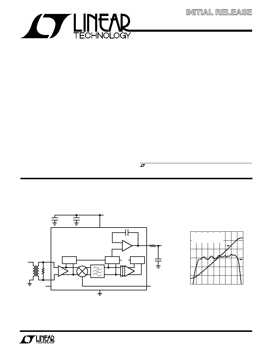
TYPICAL APPLICATIO
U
800MHz to 2.7GHz
RF Measuring Receiver
January 2002
The LT
®
5504 is an 800MHz to 2700MHz monolithic inte-
grated measuring receiver, capable of detecting a wide
dynamic range RF signal from 75dBm to +5dBm. The
logarithm of the RF signal is precisely converted into a
linear DC voltage. The LT5504 consists of RF/IF limiters,
an LO buffer amplifier, a limiting mixer, a 3rd-order
450MHz integrated low pass filter, RF/IF detectors and an
output interface. The ultrawide dynamic range is achieved
by simultaneously measuring the RF signal and a down-
converted IF signal obtained using the on-chip mixer and
an external local oscillator. The RF- and IF-detected sig-
nals are summed to generate an accurate linear DC voltage
proportional to the input RF voltage (or power) in dB. The
output is buffered with a low output impedance driver.
, LTC and LT are registered trademarks of Linear Technology Corporation.
5504 TA01a
· · ·
RF+
RF
V
OUT
R1
82
RF
INPUT
ENABLE
GND
LO
LO
INPUT
OUTPUT
C3
10pF
C1
100pF
R2
200
EN
3V
V
CC
C2
1nF
LT5504
RF
DETECTOR
IF
DETECTOR
IF
DETECTOR
Output Voltage and Slope
Variation vs RF Input Power
PIN (dBm)
80
V
OUT
(V)
SLOPE VARIATION (dB)
2.4
2.0
1.6
1.2
0.8
0.4
0
60
40 30
10
5504 TA01b
70
50
20 10
0
6
4
2
0
2
4
6
f
RF
= 900MHz
f
IF
= 240MHz
AVERAGE SLOPE:23mV/dB
LT5504
2
5504i
Power Supply Voltage ............................................ 5.5V
V
OUT
, EN ................................................................ 0,V
CC
LO Input Power .................................................... 6dBm
RF Input Power Differential (50
, 5.5V) ............. 24dBm
RF Input Power Single-Ended (50
, 5.5V) ......... 18dBm
Operating Ambient Temperature ..............40
°
C to 85
°
C
Storage Temperature Range ..................65
°
C to 150
°
C
Lead Temperature (Soldering, 10 sec).................. 300
°
C
ORDER PART
NUMBER
T
JMAX
= 150
°
C,
JA
= 160
°
C/W
LT5504EMS8
ABSOLUTE AXI U
RATI GS
W
W
W
U
PACKAGE/ORDER I FOR ATIO
U
U
W
(Note 1)
ELECTRICAL CHARACTERISTICS
T
A
= 25
°
C. V
CC
= 3V, P
LO
= 10dBm, unless otherwise noted. (Notes 2, 3)
Consult LTC Marketing for parts specified with wider operating temperature ranges.
1
2
3
4
V
CC
RF
+
RF
GND
8
7
6
5
V
CC
V
OUT
LO
EN
TOP VIEW
MS8 PACKAGE
8-LEAD PLASTIC MSOP
MS8 PART MARKING
LTGP
SYMBOL
PARAMETER
CONDITIONS
MIN
TYP
MAX
UNITS
RF Input
f
RF
Frequency Range
800 to 2700
MHz
Input Impedance
Note 6
DC Voltage
Internally Biased
1.7
V
LO Input
f
LO
Frequency Range
850 to 3100
MHz
Input Return Loss
Internally Matched
14
dB
DC Voltage
Internally Biased
0.82
V
P
LO
LO Power
16 to 8
dBm
LO to RF Leakage
900MHz
50
dBc
1.9GHz
45
dBc
2.5GHz
40
dBc
IF Frequency
f
IF
Frequency
50 to 450
MHz
Output Voltage at f
RF
= 900MHz, f
LO
= 1140MHz
Linear Dynamic Range (Note 4)
66
75
dB
Output Voltage
Input = 70dBm
0.4
V
Input = 20dBm
1.6
V
Input = 0dBm
2.1
V
Average Slope
Input from 50dBm to 20dBm
16
23
mV/dB
Output Voltage at f
RF
= 1900MHz, f
LO
= 2140MHz
Linear Dynamic Range (Note 4)
60
72
dB
Output Voltage
Input = 70dBm
0.35
V
Input = 20dBm
1.52
V
Input = 0dBm
1.9
V
Average Slope
Input from 50dBm to 20dBm
16
23
mV/dB
LT5504
3
5504i
Note 1: Absolute Maximum Ratings are those values beyond which the
life of a device may be impaired.
Note 2: Tests are performed as shown in the configuration of Figure 5.
Note 3: Specifications over the 40
°
C to 85
°
C temperature range are
guaranteed by design, characterization and correlation with statistical
process controls.
ELECTRICAL CHARACTERISTICS
T
A
= 25
°
C. V
CC
= 3V, P
LO
= 10dBm, unless otherwise noted. (Notes 2, 3)
Note 4: The Linear Dynamic Range is defined as the range over which the
output slope is at least 50% of the average slope from 50dBm to 20dBm.
Note 5: The output voltage is settled to the full specification within 1dB.
Note 6: Refer to Figure 1 and Applications Information.
Note 7: Refer to Pin Functions description.
SYMBOL
PARAMETER
CONDITIONS
MIN
TYP
MAX
UNITS
Output Voltage at f
RF
= 2500MHz, f
LO
= 2260MHz
Linear Dynamic Range (Note 4)
58
70
dB
Output Voltage
Input = 70dBm
0.3
V
Input = 20dBm
1.45
V
Input = 0dBm
1.8
V
Average Slope
Input from 50dBm to 20dBm
16
23
mV/dB
Output Interface
Current Drive Capability
400
µ
A
Output Noise Spectral Density
At 100KHz
3.9
µ
V/
Hz
At 10MHz
0.32
µ
V/
Hz
Output Response Time (Note 5)
RF Input Pin from No Signal to 0dBm
200
ns
Power Up/Down
t
ON
Turn ON Time (Note 5)
400
ns
Turn OFF Time (Note 5)
4
µ
s
Input Resistance
30
k
Enable Turn ON Voltage (Note 7)
0.6 · V
CC
V
Disable Turn OFF Voltage (Note 7)
0.4 · V
CC
V
Power Supply
V
CC
Supply Voltage
2.7
5.25
V
I
CC
Supply Current
14.7
22
mA
Shutdown Current
0.2
30
µ
A
LT5504
4
5504i
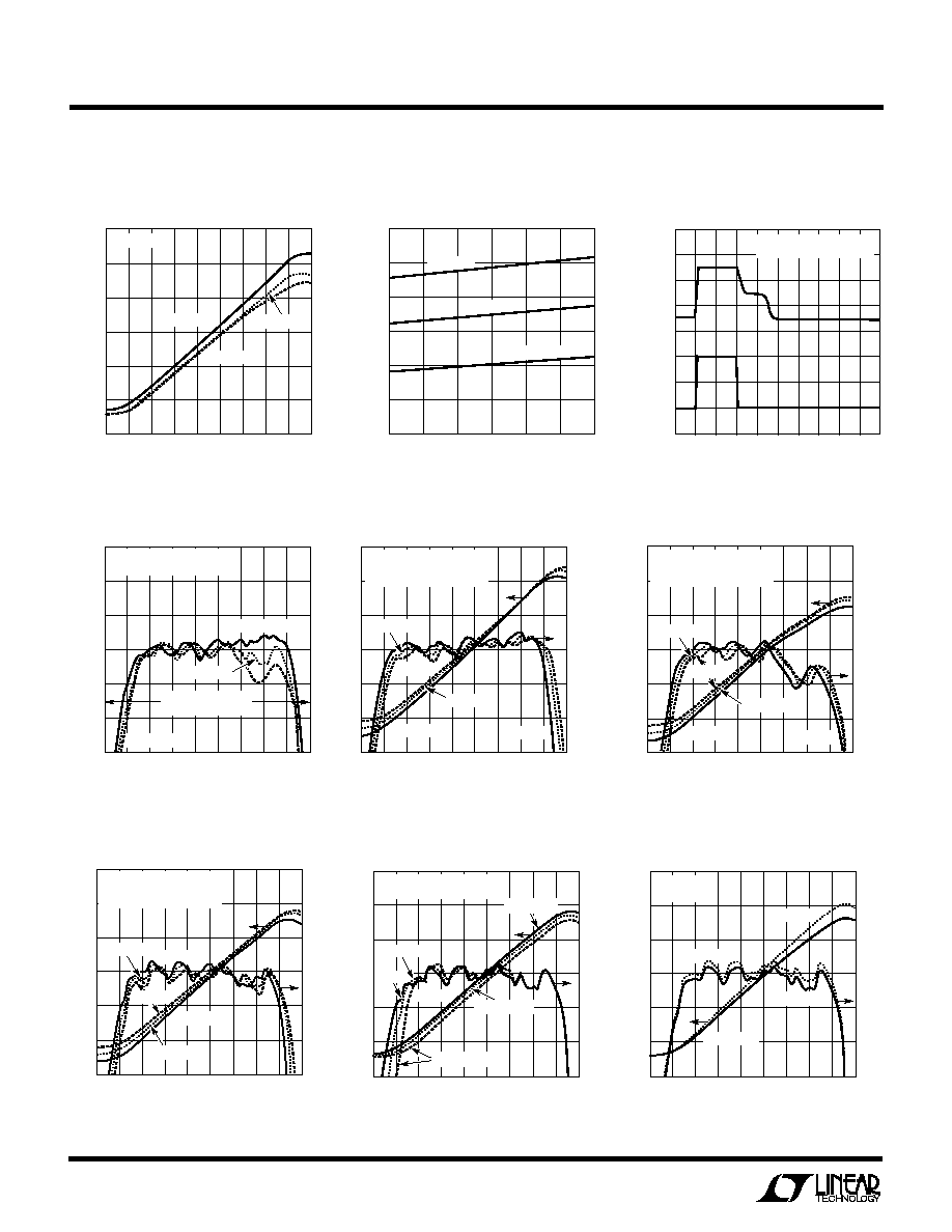
PIN (dBm)
80 70 60 50 40 30 20 10
V
OUT
(V)
2.4
2.0
1.6
1.2
0.8
0.4
0
10
5504 G09
0
f
RF
= 1.9GHz
f
IF
= 240MHz
V
CC
= 5.25V
V
CC
= 5.25V
V
CC
= 2.7V
V
CC
= 2.7V
6
4
2
0
2
4
6
SLOPE VARIATION (dB)
PIN (dBm)
80 70 60 50 40 30 20 10
V
OUT
(V)
2.4
2.0
1.6
1.2
0.8
0.4
0
10
5504 G07
0
f
RF
= 1.9GHz
f
IF
= 240MHz
AVERAGE SLOPE: 23mV/dB
T
A
= 40
°
C
T
A
= 40
°
C
6
4
2
0
2
4
6
T
A
= 25
°
C
SLOPE VARIATION (dB)
T
A
= 25
°
C
T
A
= 85
°
C
Output Voltage
vs RF Input Power and Frequency
Power Up Response Time
Supply Current vs Supply Voltage
and Temperature
Output Voltage and Slope Variation
vs RF Input Power and Temperature
Output Voltage and Slope Variation
vs RF Input Power and IF Frequency
Output Voltage and Slope Variation
vs RF Input Power and Supply Voltage
Output Voltage and Slope Variation
vs RF Input Power and Temperature
PIN (dBm)
80 70 60 50 40 30 20 10
V
OUT
(V)
2.4
2.0
1.6
1.2
0.8
0.4
0
10
5504 G01
0
f
RF
= 900MHz
f
RF
= 2.5GHz
f
IF
= 240MHz
f
RF
= 1.9GHz
SUPPLY VOLTAGE (V)
2.5
SUPPLY CURRENT (mA)
20
18
16
14
12
10
8
3.0
3.5
4.0
4.5
5504 G02
5.0
5.5
T
A
= 85
°
C
T
A
= 25
°
C
T
A
= 40
°
C
PIN (dBm)
80 70 60 50 40 30 20 10
V
OUT
(V)
2.4
2.0
1.6
1.2
0.8
0.4
0
10
5504 G05
0
f
RF
= 900MHz
f
IF
= 240MHz
AVERAGE SLOPE: 23mV/dB
T
A
= 85
°
C
T
A
= 40
°
C
T
A
= 40
°
C
6
4
2
0
2
4
2
SLOPE VARIATION (dB)
T
A
= 25
°
C
T
A
= 25
°
C
PIN (dBm)
80 70 60 50 40 30 20 10
V
OUT
(V)
2.4
2.0
1.6
1.2
0.8
0.4
0
10
5504 G08
0
f
RF
= 1.9GHz
AVERAGE SLOPE: 23mV/dB
6
4
2
0
2
4
6
SLOPE VARIATION (dB)
400MHz
240MHz
70MHz
f
IF
= 70MHz
f
IF
= 240MHz
f
IF
= 400MHz
PIN (dBm)
80 70 60 50 40 30 20 10
V
OUT
(V)
2.4
2.0
1.6
1.2
0.8
0.4
0
10
5504 G06
0
f
RF
= 2.5GHz
f
IF
= 240MHz
AVERAGE SLOPE: 23mV/dB
T
A
= 40
°
C
T
A
= 40
°
C
6
4
2
0
2
4
6
T
A
= 25
°
C
SLOPE VARIATION (dB)
T
A
= 25
°
C
T
A
= 85
°
C
5504 G03
2
µ
s/DIV
V
OUT
1V/DIV
ENABLE
1V/DIV
V
CC
= 3V
RF INPUT POWER = 0dBm
ON
OFF
Output Voltage and Slope Variation
vs RF Input Power and Temperature
TYPICAL PERFOR A CE CHARACTERISTICS
U
W
PIN (dBm)
80 70 60 50 40 30 20 10
6
4
2
0
2
4
6
10
5504 G04
0
f
RF
= 900MHz
f
RF
= 2.5GHz
f
IF
= 240MHz
AVERAGE SLOPE: 23mV/dB
50% VARIATION OR
SLOPE = 11.5mV/dB
SLOPE VARIATION (dB)
f
RF
= 1.9GHz
Output Slope Variation vs
RF Input Power and Frequency
LT5504
5
5504i
5504 G12
100ns/DIV
V
OUT
1V/DIV
PULSED
RF
900MHz
0dBm
1V/DIV
Output Voltage and Slope Variation
vs RF Input Power and Temperature
Output Voltage and Slope Variation
vs RF Input Power and Temperature
U
U
U
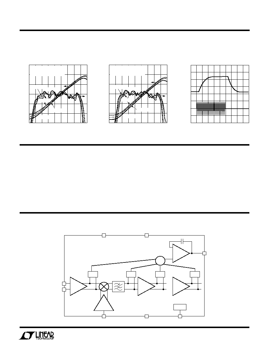
PI FU CTIO S
BLOCK DIAGRA
W
TYPICAL PERFOR A CE CHARACTERISTICS
U
W
Output Response Time
V
CC
(Pins 1, 8 ): Power Supply Pins. These pins must be
tied together at the part as close as possible, and should
be decoupled using 1000pF capacitors.
RF
+
(Pin 2): Positive RF Input Pin.
RF
(Pin 3): Negative RF Input Pin.
GND (Pin 4): Ground Pin.
EN (Pin 5): Enable Pin. The on/off threshold voltage
is about V
CC
/2. When the input voltage is higher than
0.6 · V
CC
, the circuit is completely turned on. When the
input voltage is less than 0.4 · V
CC
, the circuit is turned off.
LO (Pin 6): Local Oscillator Input Pin.
V
OUT
(Pin 7): Output Pin.
5504 BD
2
3
6
7
DET
DET
DET
DET
· · ·
LO
BUFFER
RF
LIMITER
IF
LIMITER
IF
LIMITER
LIMITING
MIXER
LPF
RF
+
RF
LO
5
EN
4
GND
1
8
V
CC
V
CC
V
OUT
+
ENABLE
PIN (dBm)
80 70 60 50 40 30 20 10
V
OUT
(V)
2.4
2.0
1.6
1.2
0.8
0.4
0
10
5504 G11
0
f
RF
= 1.9GHz
f
IF
= 400MHz
AVERAGE SLOPE: 23mV/dB
T
A
= 40
°
C
T
A
= 40
°
C
6
4
2
0
2
4
6
SLOPE VARIATION (dB)
T
A
= 25
°
C
T
A
= 85
°
C
T
A
= 25
°
C
PIN (dBm)
80 70 60 50 40 30 20 10
V
OUT
(V)
2.4
2.0
1.6
1.2
0.8
0.4
0
10
5504 G10
0
f
RF
= 1.9GHz
f
IF
= 70MHz
AVERAGE SLOPE: 23mV/dB
T
A
= 40
°
C
T
A
= 40
°
C
6
4
2
0
2
4
6
SLOPE VARIATION (dB)
T
A
= 25
°
C
T
A
= 25
°
C
T
A
= 85
°
C