 | ÐлекÑÑоннÑй компоненÑ: LT5506EUF | СкаÑаÑÑ:  PDF PDF  ZIP ZIP |
Äîêóìåíòàöèÿ è îïèñàíèÿ www.docs.chipfind.ru
LT5506
1
5506fa
IF INPUT POWER EACH TONE (dBm)
60
THD (dBc)
30
35
40
45
50
55
60
50
40
30
20
5506 TA01b
10
f
IF, 1
= 280MHz
f
IF, 2
= 280.1MHz
f
2xLO
= 570MHz
800mV
P-P
DIFFERENTIAL OUT
s
Wide Range 1.8V to 5.25V Supply
s
Frequency Range: 40MHz to 500MHz
s
4dB to 59dB Variable Power Gain
s
THD < 0.12% (58dBc)
at 800mV
P-P
Differential Output Level
s
8.8MHz I/Q Lowpass Output Noise Filters
s
IF Overload Detector
s
Baseband I/Q Amplitude Imbalance: 0.2dB
s
Baseband I/Q Phase Imbalance: 0.6
°
s
6.8dB Noise Figure at Max Gain
s
Input IP3 at Low Gain: 0.5dBm
s
Low Supply Current: 27mA
s
Low Delay Shift Over Gain Control Range: 2ps/dB
s
Outputs Biased Up While in Standby
s
16-Lead QFN 4mm x 4mm Package with Exposed Pad
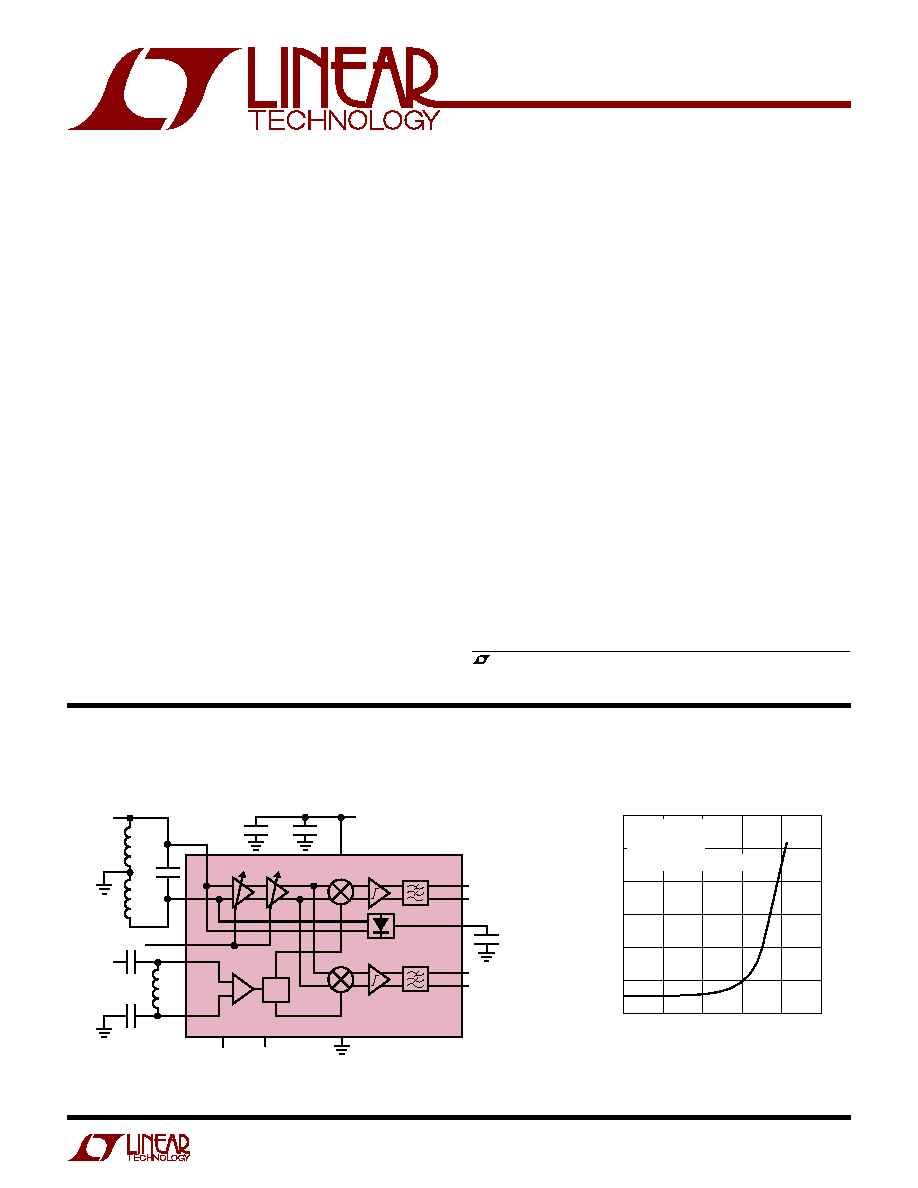
40MHz to 500MHz
Quadrature Demodulator
with VGA
, LTC and LT are registered trademarks of Linear Technology Corporation.
Total Harmonic Distortion vs
IF Input Level at 1.8V Supply
s
IEEE802.11
s
High Speed Wireless LAN
s
Wireless Local Loop
2xLO
+
2xLO
IF
+
IF
EN
STBY
V
CC
I
OUT
+
I
OUT
Q
OUT
+
Q
OUT
GND
1.8V
C2
1
µ
F
C1
1nF
C3
1.8pF
STANDBY
2xLO
560MHz
INPUT
280MHz
IF INPUT
C3
10pF
5506 TA01
÷
2
LT5506
L1
15nH
L2
15nH
L3
39nH
C5
3.3pF
C4
3.3pF
GAIN CONTROL
ENABLE
IF DET
V
CTRL
The LT
®
5506 is a 40MHz to 500MHz monolithic integrated
quadrature demodulator with variable gain amplifier (VGA),
designed for low voltage operation. It supports standards
that use a linear modulation format. The chip consists of
a VGA, quadrature down-converting mixers and lowpass
noise filters. The LO port consists of a divide-by-two stage
and LO buffers. The IC provides all building blocks for IF
down-conversion to I and Q baseband signals with a single
supply voltage of 1.8V to 5.25V. The VGA gain has a linear-
in-dB relationship to the control input voltage. Hard-clip-
ping amplifiers at the mixer outputs reduce the recovery
time from a signal overload condition. The lowpass filters
reduce the out-of-band noise and spurious frequency
components. The cut-off frequency of the noise filters is
approximately 8.8MHz. The external 2xLO frequency is
required to be twice the IF input frequency for the mixers.
The standby mode provides reduced supply current and
fast transient response into the normal operating mode
when the I/Q outputs are AC-coupled to a baseband chip.
FEATURES
DESCRIPTIO
U
APPLICATIO S
U
TYPICAL APPLICATIO
U
LT5506
2
5506fa
Supply Voltage ....................................................... 5.5V
Differential Voltage Between 2xLO
+
and 2xLO
..........
4V
IF
+
, IF
............................................. 500mV to 500mV
I
OUT
+
, I
OUT
, Q
OUT
+
, Q
OUT
.................. V
CC
1.8V to V
CC
Operating Ambient Temperature
(Note 2) ...................................................40
°
C to 85
°
C
Storage Temperature Range ..................65
°
C to 125
°
C
Voltage on Any Pin
Not to Exceed ........................ 500mV to V
CC
+ 500mV
ORDER PART
NUMBER
T
JMAX
= 125
°
C,
JA
= 37
°
C/W
EXPOSED PAD (PIN 17) IS GROUND
MUST BE SOLDERED TO PCB
LT5506EUF
ABSOLUTE AXI U
RATI GS
W
W
W
U
PACKAGE/ORDER I FOR ATIO
U
U
W
(Note 1)
ELECTRICAL CHARACTERISTICS
V
CC
= 3V. f
2xLO
= 570MHz, P
2xLO
= 5dBm (Note 5), f
IF
= 284MHz,
P
IF
= 30dBm, I and Q outputs 800mV
P-P
into 4k
differential load, T
A
= 25
°
C, EN = V
CC
, STBY = V
CC
, unless otherwise noted. (Note 3)
Consult LTC Marketing for parts specified with wider operating temperature ranges.
16 15 14 13
5
6
7
8
TOP VIEW
17
UF PACKAGE
16-LEAD (4mm
×
4mm) PLASTIC QFN
9
10
11
12
4
3
2
1
GND
IF
+
IF
GND
STBY
2xLO
+
2xLO
EN
I
OUT
+
I
OUT
Q
OUT
+
Q
OUT
V
CC
V
CTRL
IF DET
V
CC
SYMBOL
PARAMETER
CONDITIONS
MIN
TYP
MAX
UNITS
IF Input
f
IF
Frequency Range
40 to 500
MHz
Nominal Input Level
R
SOURCE
= 200
Differential
79 to 22
dBm
Input Impedance
IF
+
, IF
to GND, EN = V
CC
100
//1.2pF
IF
+
, IF
to GND, EN = GND
1pF
NF
Noise Figure at Max Gain
V
CTRL
= 1.7V
6.8
dB
G
L
Min Gain (Note 4)
V
CTRL
= 0.2V
0.9
8
dB
G
H
Max Gain (Note 4)
V
CTRL
= 1.7V
50
59
dB
IIP3
Input IP3, Min Gain
P
IF
= 22.5dBm (Note 7)
0.5
dBm
Input IP3, Max Gain
P
IF
= 75dBm (Note 7)
49
dBm
IIP2
Input IP2, Max Gain
V
CTRL
= 1.7V
8
dBm
Demodulator I/Q Output
Nominal Voltage Swing
(Note 6)
0.8
V
P-P
Clipping Level
(Note 6)
1.25
V
P-P
DC Common Mode Voltage
V
CC
1.19
V
I/Q Amplitude Imbalance
(Note 8)
0.2
0.5
dB
I/Q Phase Imbalance
(Note 8)
0.6
3
Deg
DC Offset
(Notes 6, 8)
28
mV
Output Driving Capability
Single Ended, C
LOAD
10pF
2
1.5
k
STBY to Turn-On Delay
0.3
µ
s
I/Q Output 1dB Compression
11.5
dBm
I/Q Output IM3
P
IF, 1
= 25.5dBm, 280MHz
50
dBc
P
IF, 2
= 25.5dBm, 280.1MHz (Note 7)
LT5506
3
5506fa
V
CC
= 3V. f
2
×
LO
= 570MHz, P
2
×
LO
= 5dBm (Note 5), f
IF
= 284MHz,
P
IF
= 30dBm, I and Q outputs 800mV
P-P
into 4k
differential load, T
A
= 25
°
C, EN = V
CC
, STBY = V
CC
, unless otherwise noted. (Note 3)
ELECTRICAL CHARACTERISTICS
Note 1: Absolute Maximum Ratings are those values beyond which the life
of a device may be impaired.
Note 2: Specifications over the 40
°
C to 85
°
C temperature range are
assured by design, characterization and correlation with statistical process
controls.
Note 3: Tests are performed as shown in the configuration of Figure 6. The
IF input transformer loss is substracted from the measured values.
Note 4: Power gain is defined here as the I (or Q) output power into a 4k
differential load, divided by the IF input power in dB. To calculate the
voltage gain between the differential I output (or Q output) and the IF
input, including ideal matching network, 10 · log(4k
/50) = 19dB has to
be added to this power gain.
SYMBOL
PARAMETER
CONDITIONS
MIN
TYP
MAX
UNITS
Variable Gain Amplifier (VGA)
Gain Slope Linearity Error
V
CTRL
= 0V to 1.4V
±
0.5
dB
Temperature Gain Shift
T = 40
°
C to 85
°
C, V
CTRL
= 0V to 1.4V
±
0.3
dB
Gain Control Response Time
Settled within 10% of Final Value
100
ns
Gain Control Voltage Range
0 to 1.7
V
Gain Control Slope
43
dB/V
Gain Control Input Impedance
To Internal 0.2V
25
k
Delay Shift Over Gain Control
Measured Over 10dB Step
2
ps/dB
Baseband Lowpass Filter
3dB Cutoff Frequency
7.2
8.8
10.4
MHz
Group Delay Ripple
5
ns
2xLO Input
f
2xLO
Frequency Range
80 to 1000
MHz
P
2xLO
Input Power
1:2 Transformer with 240
Shunt Resistor (Note 5)
20
5
dBm
Input Power
LC Balun (Note 5)
10
dBm
Input Impedance
Differential Between 2xLO
+
and 2xLO
800
//0.4pF
DC Common Mode Voltage
V
CC
0.4
V
IF Detector
IF Detector Range
Referred to IF Input
30 to 8
dBm
Output Voltage Range
For P
IF
= 30dBm to 8dBm
0.3 to 1.2
V
Detector Response Time
With External 1.8pF Load,
100
ns
Settling within 10% of Final Value
Power Supply
V
CC
Supply Voltage
1.8
5.25
V
I
CC
Supply Current
EN = High, STBY = Low or High
26.5
36
mA
I
OFF
Shutdown Current
EN, STBY < 350mV
0.2
30
µ
A
I
STBY
Standby Current
EN = Low; STBY = High
3.6
5.5
mA
Mode
Enable
Enable Pin Voltage
EN = High
1
V
Disable
Enable Pin Voltage
EN = Low
0.5
V
Standby
Standby Pin Voltage
STBY = High
1
V
No Standby
Standby Pin Voltage
STBY = Low
0.5
V
Note 5: If a narrow-band match is used in the 2xLO path instead of a 1:2
transformer with 240
shunt resistor, 2xLO input power can be reduced
to 10dBm, without degrading the phase imbalance. See Figure 11 and
Figure 6.
Note 6: Differential between I
OUT
+
and I
OUT
(or differential between
Q
OUT
+
and Q
OUT
).
Note 7: The gain control voltage V
CTRL
is set in such a way that the
differential output voltage between I
OUT
+
and I
OUT
(or differential between
Q
OUT
+
and Q
OUT
) is 800mV
P-P
, with the given input power P
IF
.
Note 8: The typical parameter is defined as the mean of the absolute
values of the data distribution.
LT5506
4
5506fa
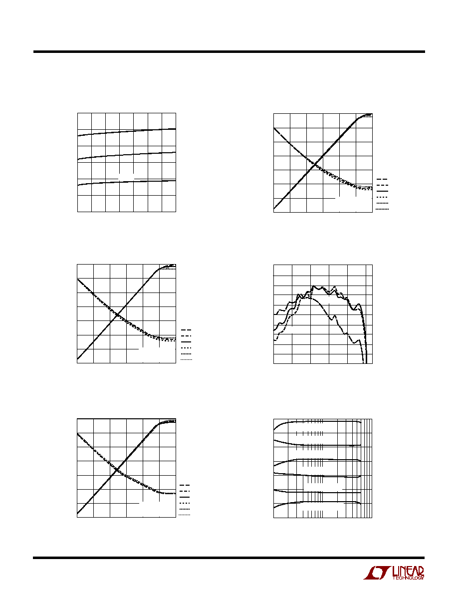
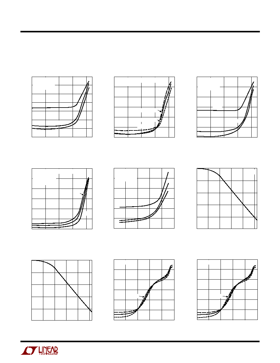
Supply Current vs Supply Voltage
Gain and Noise Figure
vs Control Voltage at 3V Supply
Gain and Noise Figure
vs Control Voltage at 1.8V Supply
Gain Flatness
vs Control Voltage at 1.8V Supply
Gain and Noise Figure
vs Control Voltage and V
CC
Gain and Noise Figure
vs IF Frequency
TYPICAL PERFOR A CE CHARACTERISTICS
U
W
SUPPLY VOLTAGE (V)
1.75
SUPPLY CURRENT (mA)
32
30
28
26
24
22
20
2.25 2.75 3.25 3.75
5506 G01
4.25 4.75 5.25
40
°
C
25
°
C
85
°
C
V
CTRL
(V)
0
G, NF (dB)
1.5
5506 G02
0.6
GAIN
NF
60
50
40
30
20
10
0
10
0.3
0.9
1.2
1.8
GAIN AT 25
°
C
NF AT 25
°
C
GAIN AT 40
°
C
NF AT 40
°
C
GAIN AT 85
°
C
NF AT 85
°
C
f
IF
= 284MHz
f
2xLO
= 570MHz
V
CTRL
(V)
0
G, NF (dB)
1.5
5506 G03
0.6
GAIN
NF
60
50
40
30
20
10
0
10
0.3
0.9
1.2
1.8
GAIN AT 40
°
C
NF AT 40
°
C
GAIN AT 25
°
C
NF AT 25
°
C
GAIN AT 85
°
C
NF AT 85
°
C
f
IF
= 284MHz
f
2xLO
= 570MHz
V
CTRL
(V)
0
0.5
GAIN DEVIATIN FROM LINEAR FIT (dB)
0.3
0.1
0.1
0.3
0.6
0.9
5506 G04
1.2
0.3
0.5
0.4
0.2
0
0.2
0.4
1.5
40
°
C
85
°
C
25
°
C
V
CTRL
(V)
0
G, NF (dB)
1.2
1.8
5506 G05
0.3
GAIN
NF
0.6
0.9
1.5
60
50
40
30
20
10
0
10
GAIN AT 1.8V
NF AT 1.8V
GAIN AT 3V
NF AT 3V
GAIN AT 5.25V
NF AT 5.25V
f
IF
= 284MHz
f
2xLO
= 570MHz
IF FREQUENCY (MHz)
10
10
0
G, NF (dB)
10
20
30
40
60
100
1000
5506 G06
50
GAIN, V
CTRL
= 1.6V
GAIN, V
CTRL
= 0.9V
GAIN, V
CTRL
= 0.2V
NF, V
CTRL
= 1.6V
NF, V
CTRL
= 0.9V
NF, V
CTRL
= 0.2V
V
CC
= 3V. f
2
×
LO
= 570MHz, P
2
×
LO
= 5dBm
(Note 5), f
IF
= 284MHz, P
IF
= 30dBm, I and Q outputs 800mV
P-P
into 4k
differential load, T
A
= 25
°
C, EN = V
CC
, STBY = V
CC
,
unless otherwise noted. (Note 3)
LT5506
5
5506fa
Total Harmonic Distortion
vs IF Input Power at 3V Supply
and 800mV
P-P
Differential Out
Total Harmonic Distortion
vs IF Input Power and IF
Frequency
Total Harmonic Distortion
vs IF Input Power at 1.8V Supply
and 800mV
P-P
Differential Out
IF INPUT POWER EACH TONE (dBm)
60
THD (dBc)
30
5506 G07
50
40
20
30
35
40
45
50
55
60
65
40
°
C
25
°
C
85
°
C
f
IF,1
= 280MHz
f
IF,2
= 280.1MHz
f
2xLO
= 570MHz
IF INPUT POWER EACH TONE (dBm)
60
THD (dBc)
30
5506 G08
50
40
20
30
35
40
45
50
55
60
f
IF
= 280MHz
f
IF
= 40MHz
800mV
P-P
DIFFERENTIAL OUT
3V SUPPLY
f
IF
= 550MHz
IF INPUT POWER EACH TONE (dBm)
60
THD (dBc)
30
5506 G09
50
40
20
30
35
40
45
50
55
60
f
IF,1
= 280MHz
f
IF,2
= 280.1MHz
f
2xLO
= 570MHz
25
°
C
40
°
C
85
°
C
Total Harmonic Distortion vs IF
Input Power and Supply Voltage
IF INPUT POWER EACH TONE (dBm)
60
THD (dBc)
30
5506 G10
50
40
20
30
35
40
45
50
55
60
3V
1.8V
5.25V
800mV
P-P
DIFFERENTIAL OUT
f
IF,1
= 280MHz
f
IF,2
= 280.1MHz
f
2xLO
= 570MHz
LPF Frequency Response
vs Baseband Frequency
and Temperature
LPF Frequency Response
vs Baseband Frequency and
Supply Voltage
Total Harmonic Distortion
vs IF Input Power at 500mV
P-P
Differential Out
IF INPUT POWER EACH TONE (dBm)
45
70
THD (dBc)
65
60
55
50
45
40
40
35
30
40
°
C
25
°
C
85
°
C
25
5506 G11
20
f
IF,1
= 280MHz
f
IF,2
= 280.1MHz
f
2xLO
= 570MHz
BASEBAND FREQUENCY (MHz)
0
25
MAGNITUDE (dB)
20
15
10
5
0
5
10
25
°
C
85
°
C
40
°
C
15
20
5505 G12
25
V
CC
= 3V
BASEBAND FREQUENCY (MHz)
0
25
MAGNITUDE (dB)
20
15
10
5
0
5
10
3V
1.8V
5.25V
15
20
5505 G13
25
IF INPUT CW POWER (dBm)
40
0.2
IF DET OUTPUT (V)
0.4
0.6
0.8
1.0
1.2
1.4
30
85
°
C
40
°
C
20
10
0
5506 G14
10
25
°
C
f
IF
= 280MHz
IF INPUT CW POWER (dBm)
40
0.2
IF DET OUTPUT (V)
0.4
0.6
0.8
1.0
1.2
1.4
30
85
°
C
40
°
C
20
10
0
5506 G15
10
25
°
C
f
IF
= 280MHz
IF Detector Output Voltage vs
IF Input CW Power at 3V Supply
IF Detector Output Voltage vs
IF Input CW Power at 1.8V Supply
TYPICAL PERFOR A CE CHARACTERISTICS
U
W
V
CC
= 3V. f
2
×
LO
= 570MHz, P
2
×
LO
= 5dBm
(Note 5), f
IF
= 284MHz, P
IF
= 30dBm, I and Q outputs 800mV
P-P
into 4k
differential load, T
A
= 25
°
C, EN = V
CC
, STBY = V
CC
,
unless otherwise noted. (Note 3)