 | ÐлекÑÑоннÑй компоненÑ: LT5519 | СкаÑаÑÑ:  PDF PDF  ZIP ZIP |
Äîêóìåíòàöèÿ è îïèñàíèÿ www.docs.chipfind.ru
LT5519
1
5519f
s
Wide RF Frequency Range: 0.7GHz to 1.4GHz
s
17.1dBm Typical Input IP3 at 1GHz
s
On-Chip RF Output Transformer
s
On-Chip 50
Matched LO and RF Ports
s
Single-Ended LO and RF Operation
s
Integrated LO Buffer: 5dBm Drive Level
s
Low LO to RF Leakage: 44dBm Typical
s
Noise Figure: 13.6dB
s
Wide IF Frequency Range: 1MHz to 400MHz
s
Enable Function with Low Off-State Leakage Current
s
Single 5V Supply
s
Small 16-Lead QFN Plastic Package
0.7GHz to 1.4GHz
High Linearity
Upconverting Mixer
The LT
®
5519 mixer is designed to meet the high linearity
requirements of wireless and cable infrastructure trans-
mission systems. A high speed, internally 50
matched,
LO amplifier drives a double-balanced mixer core, allow-
ing the use of a low power, single-ended LO source. An RF
output transformer is integrated, thus eliminating the
need for external matching components at the RF output,
while reducing system cost, component count, board area
and system-level variations. The IF port can be easily
matched to a broad range of frequencies for use in many
different applications.
The LT5519 mixer delivers +17.1dBm typical input 3rd
order intercept point at 1GHz with IF input signal levels of
10dBm. The input 1dB compression point is typically
+5.5dBm. The IC requires only a single 5V supply.
, LTC and LT are registered trademarks of Linear Technology Corporation.
Figure 1. Frequency Conversion in Wireless Infrastructure Transmitter
RF Output Power, IM3 and IM2
vs IF Input Power (Two Input Tones)
IF
+
IF
LO
LO
+
RF
+
RF
PA
LO INPUT
5dBm
BIAS
EN
V
CC1
V
CC2
V
CC3
10pF
5pF
5pF
85
5V
DC
5519 F01a
BPF
BPF
GND
4:1
220pF
220pF
33pF
100
100
(OPTIONAL)
LT5519
1
µ
F
1000pF
39nH
s
Wireless Infrastructure
s
Cable Downlink Infrastructure
s
Point-to-Point and Point-to-Multipoint Data
Communications
s
High Linearity Frequency Conversion
FEATURES
DESCRIPTIO
U
APPLICATIO S
U
TYPICAL APPLICATIO
U
IF INPUT POWER (dBm/TONE)
16
P
OUT
, IM3, IM2 (dBm/TONE)
30
10
10
0
5519 F01b
50
70
40
20
0
60
80
90
12
8
4
4
P
OUT
IM3
IM2
f
RF
= 1000MHz
P
LO
= 5dBm
f
LO
= 1140MHz
f
IF1
= 140MHz
f
IF2
= 141MHz
T
A
= 25
°
C
LT5519
2
5519f
Supply Voltage ....................................................... 5.5V
Enable Voltage ............................. 0.3V to (V
CC
+ 0.3V)
LO Input Power (Differential) ............................ +10dBm
LO
+
to LO
Differential DC Voltage ..........................
±
1V
LO
+
and LO
DC Common Mode Voltage ...... 1V to V
CC
IF Input Power (Differential) ............................. +10dBm
IF
+
and IF
DC Currents ........................................ 25mA
RF
+
to RF
Differential DC Voltage ......................
±
0.13V
RF
+
and RF
DC Common Mode Voltage ...... 1V to V
CC
Operating Temperature Range .................40
°
C to 85
°
C
Storage Temperature Range ................. 65
°
C to 125
°
C
Junction Temperature (T
J
).................................... 125
°
C
ORDER PART
NUMBER
UF PART
MARKING
T
JMAX
= 125
°
C,
JA
= 37
°
C/W
EXPOSED PAD (PIN 17) IS GND
MUST BE SOLDERED TO PCB
5519
LT5519EUF
ABSOLUTE AXI U
RATI GS
W
W
W
U
PACKAGE/ORDER I FOR ATIO
U
U
W
(Note 1)
ELECTRICAL CHARACTERISTICS
Consult LTC Marketing for parts specified with wider operating temperature ranges.
16 15 14 13
5
6
7
8
TOP VIEW
UF PACKAGE
16-LEAD (4mm
×
4mm) PLASTIC QFN
9
10
11
12
4
3
2
1
EN
V
CC1
V
CC2
V
CC3
GND
IF
+
IF
GND
GND
RF
+
RF
GND
GND
LO
LO
+
GND
17
PARAMETER
CONDITIONS
MIN
TYP
MAX
UNITS
IF Input Frequency Range
1 to 400
MHz
LO Input Frequency Range
300 to 1800
MHz
RF Output Frequency Range
700 to 1400
MHz
1GHz Application: V
CC
= 5V
DC
, EN = High, T
A
= 25
°
C, IF input = 140MHz at 10dBm, LO input = 1.14GHz at 5dBm, RF output measured
at 1GHz, unless otherwise noted. (Test circuit shown in Figure 2) (Notes 2, 3)
PARAMETER
CONDITIONS
MIN
TYP
MAX
UNITS
IF Input Return Loss
Z
O
= 50
, with External Matching
20
dB
LO Input Return Loss
Z
O
= 50
17
dB
RF Output Return Loss
Z
O
= 50
20
dB
LO Input Power
10 to 0
dBm
Conversion Gain
0.6
dB
Input 3rd Order Intercept
10dBm/Tone,
f = 1MHz
17.1
dBm
Input 2nd Order Intercept
10dBm, Single Tone
48
dBm
LO to RF Leakage
44
dBm
LO to IF Leakage
40
dBm
Input 1dB Compression
5.5
dBm
IF Common Mode Voltage
Internally Biased
1.77
V
DC
Noise Figure
Single-Side Band
13.6
dB
LT5519
3
5519f
(Test Circuit Shown in Figure 2) V
CC
= 5V
DC
, EN = High, T
A
= 25
°
C, unless otherwise noted. (Note 3)
Note 1: Absolute Maximum Ratings are those values beyond which the life
of a device may be impaired.
Note 2: External components on the final test circuit are optimized for
operation at f
RF
= 1GHz, f
LO
= 1.14GHz and f
IF
= 140MHz.
Note 3: Specifications over the 40
°
C to 85
°
C temperature range are
assured by design, characterization and correlation with statistical process
controls.
Note 4: Turn-On and Turn-Off times are based on the rise and fall times of
the RF output envelope from 40dBm to full power with an IF input power
of 10dBm.
DC ELECTRICAL CHARACTERISTICS
PARAMETER
CONDITIONS
MIN
TYP
MAX
UNITS
Enable (EN) Low = OFF, High = ON
Turn-On Time (Note 4)
2
µ
s
Turn-Off Time (Note 4)
6
µ
s
Input Current
V
ENABLE
= 5V
DC
1
10
µ
A
Enable = High (ON)
3
V
DC
Enable = Low (OFF)
0.5
V
DC
Power Supply Requirements (V
CC
)
Supply Voltage
4.5 to 5.25
V
DC
Supply Current
V
CC
= 5V
DC
60
70
mA
Shutdown Current
EN = Low
1
100
µ
A
TYPICAL PERFOR A CE CHARACTERISTICS
U
W
Supply Current vs Supply Voltage
Shutdown Current
vs Supply Voltage
(Test Circuit Shown in Figure 2)
SUPPLY VOLTAGE (V)
4
SUPPLY CURRENT (mA)
56
58
60
4.75
5.25
5519 G01
54
52
50
4.25
4.5
5
62
64
66
5.5
T
A
= 85
°
C
T
A
= 25
°
C
T
A
= 40
°
C
SUPPLY VOLTAGE (V)
4
0
SHUTDOWN CURRENT (
µ
A)
0.2
0.4
0.6
0.8
1.2
4.25
4.5
4.75
5
5519 G02
5.25
5.5
1.0
T
A
= 85
°
C
T
A
= 25
°
C
T
A
= 40
°
C
LT5519
4
5519f
Conversion Gain and SSB Noise
Figure vs LO Input Power
IIP3 and IIP2 vs
LO Input Power
LO-RF Leakage
vs LO Input Power
IIP3 and IIP2 vs
LO Input Power
RF Output Power and Output IM3 vs
IF Input Power (Two Input Tones)
TYPICAL PERFOR A CE CHARACTERISTICS
U
W
RF Output Power and Output IM2 vs
IF Input Power (Two Input Tones)
Conversion Gain and SSB Noise
Figure vs RF Output Frequency
IIP3 and IIP2
vs RF Output Frequency
LO-RF Leakage
vs RF Output Frequency
V
CC
= 5V
DC
, EN = High, T
A
= 25
°
C, IF input = 140MHz at 10dBm, LO input = 1.14GHz at 5dBm, RF output measured at 1000MHz,
unless otherwise noted. For 2-tone inputs: 2nd IF input = 141MHz at 10dBm. (Test Circuit Shown in Figure 2.)
RF OUTPUT FREQUENCY (MHz)
500
GAIN, NF (dB)
6
10
14
18
1300
5519 G03
2
2
4
8
12
16
0
4
6
700
900
1100
1500
HIGH SIDE LO
LOW SIDE LO
LOW SIDE AND HIGH SIDE LO
NF
GAIN
RF OUTPUT FREQUENCY (MHz)
500
13
IIP3 (dBm)
IIP2 (dBm)
15
17
19
IIP3
IIP2
21
23
25
0
10
20
30
40
50
60
700
900
1100
1300
5519 G04
1500
LOW SIDE LO
LOW SIDE LO
HIGH SIDE LO
HIGH SIDE LO
RF OUTPUT FREQUENCY (MHz)
500
LO LEAKAGE (dBm)
30
20
10
1300
5519 G05
40
50
60
700
900
1100
1500
LOW SIDE LO
HIGH SIDE LO
LO INPUT POWER (dBm)
16
GAIN (dB)
NF (dB)
8
12
16
4
5519 G06
4
0
6
10
14
2
2
4
12
16
20
NF
GAIN
8
4
10
14
18
6
2
0
12
8
6
2
T
A
= 85
°
C
T
A
= 85
°
C
T
A
= 25
°
C
T
A
= 40
°
C
T
A
= 40
°
C
T
A
= 25
°
C
LO INPUT POWER (dBm)
16
15
IIP3 (dBm)
IIP2 (dBm)
16
17
18
19
20
IIP2
IIP3
21
0
10
20
30
40
50
60
12
8
4
0
5519 G07
4
T
A
= 85
°
C
T
A
= 85
°
C
T
A
= 25
°
C
T
A
= 25
°
C
T
A
= 40
°
C
T
A
= 40
°
C
LO INPUT POWER (dBm)
16
60
LO LEAKAGE (dBm)
50
40
30
20
10
0
12
8
4
0
5519 G08
4
T
A
= 85
°
C
T
A
= 25
°
C
T
A
= 40
°
C
LO INPUT POWER (dBm)
16
15
IIP3 (dBm)
IIP2 (dBm)
16
17
18
19
20
21
0
10
20
30
40
IIP3
IIP2
50
60
12
8
4
0
5519 G09
4
LOW SIDE LO
LOW SIDE LO
HIGH SIDE LO
HIGH SIDE LO
IF INPUT POWER (dBm/TONE)
16
P
OUT
, IM3 (dBm/TONE)
30
P
OUT
IM3
10
10
0
5519 G10
50
70
40
20
0
60
80
90
12
8
4
4
T
A
= 85
°
C
T
A
= 85
°
C
T
A
= 25
°
C
T
A
= 25
°
C
T
A
= 40
°
C
T
A
= 40
°
C
IF INPUT POWER (dBm/TONE)
16
P
OUT
, IM2 (dBm/TONE)
30
P
OUT
IM2
10
10
0
5519 G11
50
70
40
20
0
60
80
90
12
8
4
4
T
A
= 85
°
C
T
A
= 85
°
C
T
A
= 25
°
C
T
A
= 25
°
C
T
A
= 40
°
C
T
A
= 40
°
C
LT5519
5
5519f
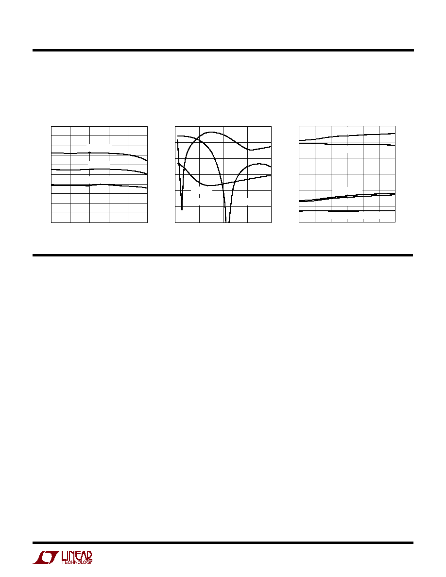
Conversion Gain vs IF Input
Power (One Input Tone)
Conversion Gain, IIP3 and IIP2
vs Supply Voltage
IF, LO and RF Port Return Loss
vs Frequency
TYPICAL PERFOR A CE CHARACTERISTICS
U
W
V
CC
= 5V
DC
, EN = High, T
A
= 25
°
C, IF input = 140MHz at 10dBm, LO input = 1.14GHz at 5dBm, RF output measured at 1000MHz,
unless otherwise noted. For 2-tone inputs: 2nd IF input = 141MHz at 10dBm. (Test Circuit Shown in Figure 2.)
IF INPUT POWER (dBm)
16
GAIN (dB)
0
2
4
0
5519 G12
2
4
1
1
3
3
5
6
12
8
4
4
T
A
= 85
°
C
T
A
= 25
°
C
T
A
= 40
°
C
FREQUENCY (MHz)
0
30
RETURN LOSS (dB)
25
20
15
10
5
0
500
1000
1500
2000
5519 G13
IF PORT
RF PORT
LO PORT
SUPPLY VOLTAGE (V)
4
2
GAIN (dB)
IIP3, IIP2 (dBm)
0
2
IIP3
IIP2
4
6
10
4.25
4.5
4.75
5
5519 G14
5.25
5.5
8
0
10
GAIN
20
30
40
60
50
LOW SIDE LO
LOW SIDE LO
LOW SIDE AND HIGH SIDE LO
HIGH SIDE LO
HIGH SIDE LO
U
U
U
PI FU CTIO S
GND (Pins 1, 4, 9, 12, 13, 16): Internal Grounds. These
pins are used to improve isolation and are not intended as
DC or RF grounds for the IC. Connect these pins to low
impedance grounds on the PCB for best performance.
IF
+
, IF
(Pins 2, 3): Differential IF Signal Inputs. A differ-
ential signal must be applied to these pins through DC
blocking capacitors. The pins must be connected to ground
with 100
resistors (the grounds must each be capable of
sinking about 18mA). For best LO leakage performance,
these pins should be DC isolated from each other. An
impedance transformation is required to match the IF in-
put to the desired source impedance (typically 50
or 75
).
EN (Pin 5): Enable Pin. When the applied voltage is greater
than 3V, the IC is enabled. When the applied voltage is less
than 0.5V, the IC is disabled and the DC current drops to
about 1
µ
A.
V
CC1
(Pin 6): Power Supply Pin for the Bias Circuits.
Typical current consumption is about 2mA. This pin
should be externally connected to V
CC
and have appropri-
ate RF bypass capacitors.
V
CC2
(Pin 7): Power Supply Pin for the LO Buffer Circuits.
Typical current consumption is about 22mA. This pin
should have appropriate RF bypass capacitors as shown
in Figure 2. The 1000pF capacitor should be located as
close to the pins as possible.
V
CC3
(Pin 8): Power Supply Pin for the Internal Mixer.
Typical current consumption is about 36mA. This pin
should be externally connected to V
CC
through an induc-
tor. A 39nH inductor is shown in Figure 2, though the value
is not critical.
RF
, RF
+
(Pins 10, 11): Differential RF Outputs. One pin
may be DC connected to a low impedance ground to realize
a 50
single-ended output. No external matching compo-
nents are required. A DC voltage should not be applied
across these pins, as they are internally connected through
a transformer winding.
LO
+
, LO
(Pins 14, 15): Differential Local Oscillator In-
puts. The LT5519 works well with a single-ended source
driving the LO
+
pin and the LO
pin connected to a low
impedance ground. No external 50
matching compo-
nents are required. An internal resistor is connected
across these pins; therefore, a DC voltage should not be
applied across the inputs.
Exposed Pad (Pin 17): DC and RF ground return for the
entire IC. This must be soldered to the printed circuit board
low impedance ground plane.