 | –≠–ª–µ–∫—Ç—Ä–æ–Ω–Ω—ã–π –∫–æ–º–ø–æ–Ω–µ–Ω—Ç: LT6204 | –°–∫–∞—á–∞—Ç—å:  PDF PDF  ZIP ZIP |

LT6202/LT6203/LT6204
1
620234fa
The LT
Æ
6202/LT6203/LT6204 are single/dual/quad low
noise, rail-to-rail input and output unity gain stable op
amps that feature 1.9nV/
Hz noise voltage and draw only
2.5mA of supply current per amplifier. These amplifiers
combine very low noise and supply current with a 100MHz
gain bandwidth product, a 25V/
µ
s slew rate, and are
optimized for low supply signal conditioning systems.
These amplifiers maintain their performance for supplies
from 2.5V to 12.6V and are specified at 3V, 5V and
±
5V
supplies. Harmonic distortion is less than ≠ 80dBc at
1MHz making these amplifiers suitable in low power data
acquisition systems.
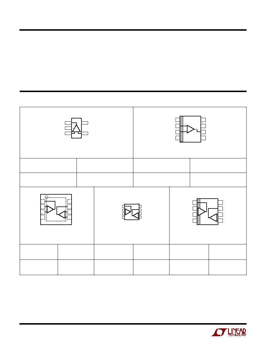
The LT6202 is available in the 5-pin SOT-23 and the 8-pin
SO, while the LT6203 comes in 8-pin SO and MSOP pack-
ages with standard op amp pinouts. For compact layouts
the LT6203 is also available in a tiny fine line leadless
package (DFN), while the quad LT6204 is available in the
16-pin SSOP and 14-pin SO packages. These devices can
be used as plug-in replacements for many op amps to
improve input/output range and noise performance.
s
Low Noise, Low Power Signal Processing
s
Active Filters
s
Rail-to-Rail Buffer Amplifiers
s
Driving A/D Converters
s
DSL Receivers
s
Battery Powered/Battery Backed Equipment
, LTC and LT are registered trademarks of Linear Technology Corporation.
s
Low Noise Voltage: 1.9nV/
Hz (100kHz)
s
Low Supply Current: 3mA/Amp Max
s
Gain Bandwidth Product: 100MHz
s
Dual LT6203 in Tiny DFN Package
s
Low Distortion: ≠80dB at 1MHz
s
Low Offset Voltage: 500
µ
V Max
s
Wide Supply Range: 2.5V to 12.6V
s
Input Common Mode Range Includes Both Rails
s
Output Swings Rail-to-Rail
s
Common Mode Rejection Ratio 90dB Typ
s
Unity Gain Stable
s
Low Noise Current: 1.1pA/
Hz
s
Output Current: 30mA Min
s
Operating Temperature Range ≠40
∞
C to 85
∞
C
Single/Dual/Quad 100MHz,
Rail-to-Rail Input and Output,
Ultralow 1.9nV/
Hz Noise, Low Power Op Amps
Low Noise 4- to 2-Wire Local Echo Cancellation Differential Receiver
Line Receiver Integrated Noise 25kHz to 150kHz
BANDWIDTH (kHz)
0
INTEGRATED NOISE (
µ
V
RMS
)
5.0
4.5
4.0
3.5
3.0
2.5
2.0
1.5
1.0
0.5
0
40
80
100
6203 ∑ TA01b
20
60
120 140
160
1:1
∑
∑
V
L
100
LINE
50
50
1k
1k
V
R
LINE
RECEIVER
2k
1k
1k
2k
6203 TA01a
≠
+
≠
+
≠
+
≠
+
V
D
LINE
DRIVER
1/2 LT6203
1/2 LT6203
1/2 LT1739
1/2 LT1739
APPLICATIO S
U
FEATURES
TYPICAL APPLICATIO
U
DESCRIPTIO
U
LT6202/LT6203/LT6204
2
620234fa
ABSOLUTE AXI U
RATI GS
W
W
W
U
Total Supply Voltage (V
+
to V
≠
) ............................ 12.6V
Input Current (Note 2) ........................................
±
40mA
Output Short-Circuit Duration (Note 3) ............ Indefinite
Operating Temperature Range (Note 4) ...≠40
∞
C to 85
∞
C
Specified Temperature Range (Note 5) ....≠40
∞
C to 85
∞
C
Junction Temperature ........................................... 150
∞
C
PACKAGE/ORDER I FOR ATIO
U
U
W
(Note 1)
Junction Temperature (DD Package) .................... 125
∞
C
Storage Temperature Range ..................≠65
∞
C to 150
∞
C
Storage Temperature Range
(DD Package) ........................................≠65
∞
C to 125
∞
C
Lead Temperature (Soldering, 10 sec).................. 300
∞
C
OUT 1
V
≠
2
TOP VIEW
S5 PACKAGE
5-LEAD PLASTIC TSOT-23
+IN 3
5 V
+
4 ≠IN
+
≠
T
JMAX
= 150
∞
C,
JA
= 250
∞
C/W
T
JMAX
= 150
∞
C,
JA
= 250
∞
C/W
1
2
3
4
OUT A
≠IN A
+IN A
V
≠
8
7
6
5
V
+
OUT B
≠IN B
+IN B
TOP VIEW
MS8 PACKAGE
8-LEAD PLASTIC MSOP
+
≠
+
≠
T
JMAX
= 150
∞
C,
JA
= 190
∞
C/W
ORDER PART
NUMBER
LT6202CS5
LT6202IS5
LTG6
S5 PART
MARKING*
MS8 PART
MARKING
LTB2
LTB3
ORDER PART
NUMBER
LT6202CS8
LT6202IS8
S8 PART
MARKING
6202
6202I
ORDER PART
NUMBER
LT6203CMS8
LT6203IMS8
T
JMAX
= 150
∞
C,
JA
= 190
∞
C/W
1
2
3
4
8
7
6
5
TOP VIEW
NC
V
+
OUT
NC
NC
≠IN
+IN
V
≠
S8 PACKAGE
8-LEAD PLASTIC SO
+
≠
TOP VIEW
DD PACKAGE
8-LEAD (3mm
◊
3mm) PLASTIC DFN
5
6
7
8
4
3
2
1
OUT A
≠IN A
+IN A
V
≠
V
+
OUT B
≠IN B
+IN B
B
A
T
JMAX
= 125
∞
C,
JA
= 160
∞
C/W
UNDERSIDE METAL CONNECTED TO V
≠
ORDER PART
NUMBER
LT6203CDD
LT6203IDD
DD PART
MARKING*
LAAP
*The temperature grades are identified by a label on the shipping container.
TOP VIEW
S8 PACKAGE
8-LEAD PLASTIC SO
1
2
3
4
8
7
6
5
OUT A
≠IN A
+IN A
V
≠
V
+
OUT B
≠IN B
+IN B
+
≠
+
≠
ORDER PART
NUMBER
LT6203CS8
LT6203IS8
S8 PART
MARKING
6203
6203I

LT6202/LT6203/LT6204
3
620234fa
TOP VIEW
S PACKAGE
14-LEAD PLASTIC SO
1
2
3
4
5
6
7
14
13
12
11
10
9
8
OUT A
≠IN A
+IN A
V
+
+IN B
≠IN B
OUT B
OUT D
≠IN D
+IN D
V
≠
+IN C
≠IN C
OUT C
+
≠
+
≠
+
≠
+
≠
A
B
C
D
T
JMAX
= 150
∞
C,
JA
= 150
∞
C/W
TOP VIEW
GN PACKAGE
16-LEAD NARROW PLASTIC SSOP
1
2
3
4
5
6
7
8
16
15
14
13
12
11
10
9
OUT A
≠IN A
+IN A
V
+
+IN B
≠IN B
OUT B
NC
OUT D
≠IN D
+IN D
V
≠
+IN C
≠IN C
OUT C
NC
+
≠
+
≠
+
≠
+
≠
A
D
B
C
T
JMAX
= 150
∞
C,
JA
= 135
∞
C/W
ORDER PART
NUMBER
LT6204CS
LT6204IS
PACKAGE/ORDER I FOR ATIO
U
U
W
6204
6204I
GN PART
MARKING
ORDER PART
NUMBER
Consult LTC Marketing for parts specified with wider operating temperature ranges.
ELECTRICAL CHARACTERISTICS
T
A
= 25
∞
C, V
S
=5V, 0V; V
S
= 3V, 0V; V
CM
= V
OUT
= half supply,
unless otherwise noted.
SYMBOL
PARAMETER
CONDITIONS
MIN
TYP
MAX
UNITS
V
OS
Input Offset Voltage
V
S
= 5V, 0V, V
CM
= Half Supply
LT6203, LT6204, LT6202S8
0.1
0.5
mV
LT6202 SOT-23
0.1
0.7
mV
V
S
= 3V, 0V, V
CM
= Half Supply
LT6203, LT6204, LT6202S8
0.6
1.5
mV
LT6202 SOT-23
0.6
1.7
mV
V
S
= 5V, 0V, V
CM
= V
+
to V
≠
LT6203, LT6204, LT6202S8
0.25
2.0
mV
LT6202 SOT-23
0.25
2.2
mV
V
S
= 3V, 0V, V
CM
= V
+
to V
≠
LT6203, LT6204, LT6202S8
1.0
3.5
mV
LT6202 SOT-23
1.0
3.7
mV
Input Offset Voltage Match
V
CM
= Half Supply
0.15
0.8
mV
(Channel-to-Channel) (Note 6)
V
CM
= V
≠
to V
+
0.3
1.8
mV
I
B
Input Bias Current
V
CM
= Half Supply
≠7.0
≠1.3
µ
A
V
CM
= V
+
1.3
2.5
µ
A
V
CM
= V
≠
≠8.8
≠3.3
µ
A
I
B
I
B
Shift
V
CM
= V
≠
to V
+
4.7
11.3
µ
A
I
B
Match (Channel-to-Channel) (Note 6)
0.1
0.6
µ
A
I
OS
Input Offset Current
V
CM
= Half Supply
0.12
1
µ
A
V
CM
= V
+
0.07
1
µ
A
V
CM
= V
≠
0.12
1.1
µ
A
Input Noise Voltage
0.1Hz to 10Hz
800
nV
P-P
e
n
Input Noise Voltage Density
f = 100kHz, V
S
= 5V
2
nV/
Hz
f = 10kHz, V
S
= 5V
2.9
4.5
nV/
Hz
i
n
Input Noise Current Density, Balanced
f = 10kHz, V
S
= 5V
0.75
pA/
Hz
Input Noise Current Density, Unbalanced
1.1
pA/
Hz
Input Resistance
Common Mode
4
M
Differential Mode
12
k
LT6204CGN
LT6204IGN
LT6202/LT6203/LT6204
4
620234fa
ELECTRICAL CHARACTERISTICS
T
A
= 25
∞
C, V
S
=5V, 0V; V
S
= 3V, 0V; V
CM
= V
OUT
= half supply,
unless otherwise noted.
SYMBOL
PARAMETER
CONDITIONS
MIN
TYP
MAX
UNITS
C
IN
Input Capacitance
Common Mode
1.8
pF
Differential Mode
1.5
pF
A
VOL
Large Signal Gain
V
S
= 5V, V
O
= 0.5V to 4.5V, R
L
= 1k to V
S
/2
40
70
V/mV
V
S
= 5V, V
O
= 1V to 4V, R
L
= 100 to V
S
/2
8.0
14
V/mV
V
S
= 3V, V
O
= 0.5V to 2.5V, R
L
= 1k to V
S
/2
17
40
V/mV
CMRR
Common Mode Rejection Ratio
V
S
= 5V, V
CM
= V
≠
to V
+
60
83
dB
V
S
= 5V, V
CM
= 1.5V to 3.5V
80
100
dB
V
S
= 3V, V
CM
= V
≠
to V
+
56
80
dB
CMRR Match (Channel-to-Channel) (Note 6)
V
S
= 5V, V
CM
= 1.5V to 3.5V
85
120
dB
PSRR
Power Supply Rejection Ratio
V
S
= 2.5V to 10V, V
CM
= 0V
60
74
dB
PSRR Match (Channel-to-Channel) (Note 6)
V
S
= 2.5V to 10V, V
CM
= 0V
70
100
dB
Minimum Supply Voltage (Note 7)
2.5
V
V
OL
Output Voltage Swing LOW Saturation
No Load
5
50
mV
(Note 8)
I
SINK
= 5mA
85
190
mV
V
S
= 5V, I
SINK
= 20mA
240
460
mV
V
S
= 3V, I
SINK
= 15mA
185
350
mV
V
OH
Output Voltage Swing HIGH Saturation
No Load
25
75
mV
(Note 8)
I
SOURCE
= 5mA
90
210
mV
V
S
= 5V, I
SOURCE
= 20mA
325
600
mV
V
S
= 3V, I
SOURCE
= 15mA
225
410
mV
I
SC
Short-Circuit Current
V
S
= 5V
±
30
±
45
mA
V
S
= 3V
±
25
±
40
mA
I
S
Supply Current per Amp
V
S
= 5V
2.5
3.0
mA
V
S
= 3V
2.3
2.85
mA
GBW
Gain Bandwidth Product
Frequency = 1MHz, V
S
= 5V
90
MHz
SR
Slew Rate
V
S
= 5V, A
V
= ≠1, R
L
= 1k, V
O
= 4V
17
24
V/
µ
s
FPBW
Full Power Bandwidth (Note 10)
V
S
= 5V, V
OUT
= 3V
P-P
1.8
2.5
MHz
t
S
Settling Time
0.1%, V
S
= 5V, V
STEP
= 2V, A
V
= ≠1, R
L
= 1k
85
ns
The
q
denotes the specifications which apply over 0
∞
C < T
A
< 70
∞
C temperature range. V
S
= 5V, 0V; V
S
= 3V, 0V;
V
CM
= V
OUT
= half supply, unless otherwise noted.
SYMBOL
PARAMETER
CONDITIONS
MIN
TYP
MAX
UNITS
V
OS
Input Offset Voltage
V
S
= 5V, 0V, V
CM
= Half Supply
LT6203, LT6204, LT6202S8
q
0.2
0.7
mV
LT6202 SOT-23
q
0.2
0.9
mV
V
S
= 3V, 0V, V
CM
= Half Supply
LT6203, LT6204, LT6202S8
q
0.6
1.7
mV
LT6202 SOT-23
q
0.6
1.9
mV
V
S
= 5V, 0V, V
CM
= V
+
to V
≠
LT6203, LT6204, LT6202S8
q
0.7
2.5
mV
LT6202 SOT-23
q
0.7
2.7
mV
V
S
= 3V, 0V, V
CM
= V
+
to V
≠
LT6203, LT6204, LT6202S8
q
1.2
4.0
mV
LT6202 SOT-23
q
1.2
4.2
mV
V
OS
TC
Input Offset Voltage Drift (Note 9)
V
CM
= Half Supply
q
3.0
9.0
µ
V/
∞
C
Input Offset Voltage Match
V
CM
= Half Supply
q
0.15
0.9
mV
(Channel-to-Channel) (Note 6)
V
CM
= V
≠
to V
+
q
0.5
2.3
mV

LT6202/LT6203/LT6204
5
620234fa
SYMBOL
PARAMETER
CONDITIONS
MIN
TYP
MAX
UNITS
I
B
Input Bias Current
V
CM
= Half Supply
q
≠7.0
≠1.3
µ
A
V
CM
= V
+
q
1.3
2.5
µ
A
V
CM
= V
≠
q
≠8.8
≠3.3
µ
A
I
B
I
B
Shift
V
CM
= V
≠
to V
+
q
4.7
11.3
µ
A
I
B
Match (Channel-to-Channel) (Note 6)
q
0.1
0.6
µ
A
I
OS
Input Offset Current
V
CM
= Half Supply
q
0.15
1
µ
A
V
CM
= V
+
q
0.10
1
µ
A
V
CM
= V
≠
q
0.15
1.1
µ
A
A
VOL
Large Signal Gain
V
S
= 5V, V
O
= 0.5V to 4.5V, R
L
= 1k to V
S
/2
q
35
60
V/mV
V
S
= 5V, V
O
= 1.5V to 3.5V, R
L
= 100 to V
S
/2
q
6.0
12
V/mV
V
S
= 3V, V
O
= 0.5V to 2.5V, R
L
= 1k to V
S
/2
q
15
36
V/mV
CMRR
Common Mode Rejection Ratio
V
S
= 5V, V
CM
= V
≠
to V
+
q
60
83
dB
V
S
= 5V, V
CM
= 1.5V to 3.5V
q
78
97
dB
V
S
= 3V, V
CM
= V
≠
to V
+
q
56
75
dB
CMRR Match (Channel-to-Channel) (Note 6) V
S
= 5V, V
CM
= 1.5V to 3.5V
q
83
100
dB
PSRR
Power Supply Rejection Ratio
V
S
= 3V to 10V, V
CM
= 0V
q
60
70
dB
PSRR Match (Channel-to-Channel) (Note 6)
V
S
= 3V to 10V, V
CM
= 0V
q
70
100
dB
Minimum Supply Voltage (Note 7)
q
3.0
V
V
OL
Output Voltage Swing LOW Saturation
No Load
q
5.0
60
mV
(Note 8)
I
SINK
= 5mA
q
95
200
mV
I
SINK
= 15mA
q
260
365
mV
V
OH
Output Voltage Swing HIGH Saturation
No Load
q
50
100
mV
(Note 8)
I
SOURCE
= 5mA
q
115
230
mV
V
S
= 5V, I
SOURCE
= 20mA
q
360
635
mV
V
S
= 3V, I
SOURCE
= 15mA
q
260
430
mV
I
SC
Short-Circuit Current
V
S
= 5V
q
±
20
±
33
mA
V
S
= 3V
q
±
20
±
30
mA
I
S
Supply Current per Amp
V
S
= 5V
q
3.1
3.85
mA
V
S
= 3V
q
2.75
3.50
mA
GBW
Gain Bandwidth Product
Frequency = 1MHz
q
87
MHz
SR
Slew Rate
V
S
= 5V, A
V
= ≠1, R
L
= 1k, V
O
= 4V
q
15
21
V/
µ
s
FPBW
Full Power Bandwidth (Note 10)
V
S
= 5V, V
OUT
= 3V
P-P
q
1.6
2.2
MHz
The
q
denotes the specifications which apply over 0
∞
C < T
A
< 70
∞
C
temperature range. V
S
= 5V, 0V; V
S
= 3V, 0V; V
CM
= V
OUT
= half supply, unless otherwise noted.
ELECTRICAL CHARACTERISTICS
SYMBOL
PARAMETER
CONDITIONS
MIN
TYP
MAX
UNITS
V
OS
Input Offset Voltage
V
S
= 5V, 0V, V
CM
= Half Supply
LT6203, LT6204, LT6202S8
q
0.2
0.8
mV
LT6202 SOT-23
q
0.2
1.0
mV
V
S
= 3V, 0V, V
CM
= Half Supply
LT6203, LT6204, LT6202S8
q
0.6
2.0
mV
LT6202 SOT-23
q
0.6
2.2
mV
V
S
= 5V, 0V, V
CM
= V
+
to V
≠
LT6203, LT6204, LT6202S8
q
1.0
3.0
mV
LT6202 SOT-23
q
1.0
3.5
mV
V
S
= 3V, 0V, V
CM
= V
+
to V
≠
LT6203, LT6204, LT6202S8
q
1.4
4.5
mV
LT6202 SOT-23
q
1.4
4.7
mV
The
q
denotes the specifications which apply over ≠40
∞
C < T
A
< 85
∞
C temperature range. V
S
= 5V, 0V; V
S
= 3V, 0V; V
CM
= V
OUT
= half
supply, unless otherwise noted. (Note 5)

LT6202/LT6203/LT6204
6
620234fa
SYMBOL
PARAMETER
CONDITIONS
MIN
TYP
MAX
UNITS
V
OS
TC
Input Offset Voltage Drift (Note 9)
V
CM
= Half Supply
q
3.0
9.0
µ
V/
∞
C
Input Offset Voltage Match
V
CM
= Half Supply
q
0.3
1.0
mV
(Channel-to-Channel) (Note 6)
V
CM
= V
≠
to V
+
q
0.7
2.5
mV
I
B
Input Bias Current
V
CM
= Half Supply
q
≠7.0
≠1.3
µ
A
V
CM
= V
+
q
1.3
2.5
µ
A
V
CM
= V
≠
q
≠8.8
≠3.3
µ
A
I
B
I
B
Shift
V
CM
= V
≠
to V
+
q
4.7
11.3
µ
A
I
B
Match (Channel-to-Channel) (Note 6)
q
0.1
0.6
µ
A
I
OS
Input Offset Current
V
CM
= Half Supply
q
0.2
1
µ
A
V
CM
= V
+
q
0.2
1.1
µ
A
V
CM
= V
≠
q
0.2
1.2
µ
A
A
VOL
Large Signal Gain
V
S
= 5V, V
O
= 0.5V to 4.5V, R
L
= 1k to V
S
/2
q
32
60
V/mV
V
S
= 5V, V
O
= 1.5V to 3.5V, R
L
= 100 to V
S
/2
q
4.0
10
V/mV
V
S
= 3V, V
O
= 0.5V to 2.5V, R
L
= 1k to V
S
/2
q
13
32
V/mV
CMRR
Common Mode Rejection Ratio
V
S
= 5V, V
CM
= V
≠
to V
+
q
60
80
dB
V
S
= 5V, V
CM
= 1.5V to 3.5V
q
75
95
dB
V
S
= 3V, V
CM
= V
≠
to V
+
q
56
75
dB
CMRR Match (Channel-to-Channel) (Note 6) V
S
= 5V, V
CM
= 1.5V to 3.5V
q
80
100
dB
PSRR
Power Supply Rejection Ratio
V
S
= 3V to 10V, V
CM
= 0V
q
60
70
dB
PSRR Match (Channel-to-Channel) (Note 6)
V
S
= 3V to 10V, V
CM
= 0V
q
70
100
dB
Minimum Supply Voltage (Note 7)
q
3.0
V
V
OL
Output Voltage Swing LOW Saturation
No Load
q
6
70
mV
(Note 8)
I
SINK
= 5mA
q
95
210
mV
I
SINK
= 15mA
q
210
400
mV
V
OH
Output Voltage Swing HIGH Saturation
No Load
q
55
110
mV
(Note 8)
I
SOURCE
= 5mA
q
125
240
mV
V
S
= 5V, I
SOURCE
= 15mA
q
370
650
mV
V
S
= 3V, I
SOURCE
= 15mA
q
270
650
mV
I
SC
Short-Circuit Current
V
S
= 5V
q
±
15
±
25
mA
V
S
= 3V
q
±
15
±
23
mA
I
S
Supply Current per Amp
V
S
= 5V
q
3.3
4.1
mA
V
S
= 3V
q
3.0
3.65
mA
GBW
Gain Bandwidth Product
Frequency = 1MHz
q
83
MHz
SR
Slew Rate
V
S
= 5V, A
V
= ≠1, R
L
= 1k, V
O
= 4V
q
12
17
V/
µ
s
FPBW
Full Power Bandwidth (Note 10)
V
S
= 5V, V
OUT
= 3V
P-P
q
1.3
1.8
MHz
The
q
denotes the specifications which apply over ≠40
∞
C < T
A
< 85
∞
C
temperature range. V
S
= 5V, 0V; V
S
= 3V, 0V; V
CM
= V
OUT
= half supply, unless otherwise noted. (Note 5)
ELECTRICAL CHARACTERISTICS
LT6202/LT6203/LT6204
7
620234fa
SYMBOL
PARAMETER
CONDITIONS
MIN
TYP
MAX
UNITS
V
OS
Input Offset Voltage
LT6203, LT6204, LT6202S8
V
CM
= 0V
1.0
2.5
mV
V
CM
= V
+
2.6
5.5
mV
V
CM
= V
≠
2.3
5.0
mV
LT6202 SOT-23
V
CM
= 0V
1.0
2.7
mV
V
CM
= V
+
2.6
6.0
mV
V
CM
= V
≠
2.3
5.5
mV
Input Offset Voltage Match
V
CM
= 0V
0.2
1.0
mV
(Channel-to-Channel) (Note 6)
V
CM
= V
≠
to V
+
0.4
2.0
mV
I
B
Input Bias Current
V
CM
= Half Supply
≠7.0
≠1.3
µ
A
V
CM
= V
+
1.3
3.0
µ
A
V
CM
= V
≠
≠9.5
≠3.8
µ
A
I
B
I
B
Shift
V
CM
= V
≠
to V
+
5.3
12.5
µ
A
I
B
Match (Channel-to-Channel) (Note 6)
0.1
0.6
µ
A
I
OS
Input Offset Current
V
CM
= Half Supply
0.15
1
µ
A
V
CM
= V
+
0.2
1.2
µ
A
V
CM
= V
≠
0.35
1.3
µ
A
Input Noise Voltage
0.1Hz to 10Hz
800
nV
P-P
e
n
Input Noise Voltage Density
f = 100kHz
1.9
nV/
Hz
f = 10kHz
2.8
4.5
nV/
Hz
i
n
Input Noise Current Density, Balanced
f = 10kHz
0.75
pA/
Hz
Input Noise Current Density, Unbalanced
1.1
pA/
Hz
Input Resistance
Common Mode
4
M
Differential Mode
12
k
C
IN
Input Capacitance
Common Mode
1.8
pF
Differential Mode
1.5
pF
A
VOL
Large Signal Gain
V
O
=
±
4.5V, R
L
= 1k
75
130
V/mV
V
O
=
±
2.5V, R
L
= 100
11
19
V/mV
CMRR
Common Mode Rejection Ratio
V
CM
= V
≠
to V
+
65
85
dB
V
CM
= ≠2V to 2V
85
98
dB
CMRR Match (Channel-to-Channel) (Note 6)
V
CM
= ≠2V to 2V
85
120
dB
PSRR
Power Supply Rejection Ratio
V
S
=
±
1.25V to
±
5V
60
74
dB
PSRR Match (Channel-to-Channel) (Note 6)
V
S
=
±
1.25V to
±
5V
70
100
dB
V
OL
Output Voltage Swing LOW Saturation
No Load
5
50
mV
(Note 8)
I
SINK
= 5mA
87
190
mV
I
SINK
= 20mA
245
460
mV
V
OH
Output Voltage Swing HIGH Saturation
No Load
40
95
mV
(Note 8)
I
SOURCE
= 5mA
95
210
mV
I
SOURCE
= 20mA
320
600
mV
I
SC
Short-Circuit Current
±
30
±
40
mA
I
S
Supply Current per Amp
2.8
3.5
mA
GBW
Gain Bandwidth Product
Frequency = 1MHz
70
100
MHz
SR
Slew Rate
A
V
= ≠1, R
L
= 1k, V
O
= 4V
18
25
V/
µ
s
FPBW
Full Power Bandwidth (Note 10)
V
OUT
= 3V
P-P
1.9
2.6
MHz
t
S
Settling Time
0.1%, V
STEP
= 2V, A
V
= ≠1, R
L
= 1k
78
ns
dG
Differential Gain (Note 11)
A
V
= 2, R
F
= R
G
= 499
, R
L
= 2k
0.05
%
dP
Differential Phase (Note 11)
A
V
= 2, R
F
= R
G
= 499
, R
L
= 2k
0.03
DEG
T
A
= 25
∞
C, V
S
=
±
5V; V
CM
= V
OUT
= 0V, unless otherwise noted.
ELECTRICAL CHARACTERISTICS
LT6202/LT6203/LT6204
8
620234fa
SYMBOL
PARAMETER
CONDITIONS
MIN
TYP
MAX
UNITS
V
OS
Input Offset Voltage
LT6203, LT6204, LT6202S8
V
CM
= 0V
q
1.6
2.8
mV
V
CM
= V
+
q
3.2
6.8
mV
V
CM
= V
≠
q
2.8
5.8
mV
LT6202 SOT-23
V
CM
= 0V
q
1.6
3.0
mV
V
CM
= V
+
q
3.2
7.3
mV
V
CM
= V
≠
q
2.8
6.3
mV
V
OS
TC
Input Offset Voltage Drift (Note 9)
V
CM
= Half Supply
q
7.5
24
µ
V/
∞
C
Input Offset Voltage Match
V
CM
= 0V
q
0.2
1.0
mV
(Channel-to-Channel) (Note 6)
V
CM
= V
≠
to V
+
q
0.5
2.2
mV
I
B
Input Bias Current
V
CM
= Half Supply
q
≠7.0
≠1.4
µ
A
V
CM
= V
+
q
1.8
3.6
µ
A
V
CM
= V
≠
q
≠10
≠4.3
µ
A
I
B
I
B
Shift
V
CM
= V
≠
to V
+
q
5.4
13
µ
A
I
B
Match (Channel-to-Channel) (Note 6)
q
0.15
0.7
µ
A
I
OS
Input Offset Current
V
CM
= Half Supply
q
0.1
1
µ
A
V
CM
= V
+
q
0.2
1.2
µ
A
V
CM
= V
≠
q
0.4
1.4
µ
A
A
VOL
Large Signal Gain
V
O
=
±
4.5V, R
L
= 1k
q
70
120
V/mV
V
O
=
±
2V, R
L
= 100
q
10
18
V/mV
CMRR
Common Mode Rejection Ratio
V
CM
= V
≠
to V
+
q
65
84
dB
V
CM
= ≠2V to 2V
q
83
95
dB
CMRR Match (Channel-to-Channel) (Note 6)
V
CM
= ≠2V to 2V
q
83
110
dB
PSRR
Power Supply Rejection Ratio
V
S
=
±
1.5V to
±
5V
q
60
70
dB
PSRR Match (Channel-to-Channel) (Note 6)
V
S
=
±
1.5V to
±
5V
q
70
100
dB
V
OL
Output Voltage Swing LOW Saturation
No Load
q
6
70
mV
(Note 8)
I
SINK
= 5mA
q
95
200
mV
I
SINK
= 15mA
q
210
400
mV
V
OH
Output Voltage Swing HIGH Saturation
No Load
q
65
120
mV
(Note 8)
I
SOURCE
= 5mA
q
125
240
mV
I
SOURCE
= 20mA
q
350
625
mV
I
SC
Short-Circuit Current
q
±
25
±
34
mA
I
S
Supply Current per Amp
q
3.5
4.3
mA
GBW
Gain Bandwidth Product
Frequency = 1MHz
q
95
MHz
SR
Slew Rate
A
V
= ≠1, R
L
= 1k, V
O
= 4V
q
16
22
V/
µ
s
FPBW
Full Power Bandwidth (Note 10)
V
OUT
= 3V
P-P
q
1.7
2.3
MHz
The
q
denotes the specifications which apply over 0
∞
C < T
A
< 70
∞
C
temperature range. V
S
=
±
5V; V
CM
= V
OUT
= 0V, unless otherwise noted.
ELECTRICAL CHARACTERISTICS
SYMBOL
PARAMETER
CONDITIONS
MIN
TYP
MAX
UNITS
V
OS
Input Offset Voltage
LT6203, LT6204, LT6202S8
V
CM
= 0V
q
1.7
3.0
mV
V
CM
= V
+
q
3.8
7.5
mV
V
CM
= V
≠
q
3.5
6.6
mV
LT6202 SOT-23
V
CM
= 0V
q
1.7
3.2
mV
V
CM
= V
+
q
3.8
7.7
mV
V
CM
= V
≠
q
3.5
6.7
mV
The
q
denotes the specifications which apply over ≠40
∞
C < T
A
< 85
∞
C temperature range. V
S
=
±
5V; V
CM
= V
OUT
= 0V, unless otherwise
noted. (Note 5)

LT6202/LT6203/LT6204
9
620234fa
SYMBOL
PARAMETER
CONDITIONS
MIN
TYP
MAX
UNITS
V
OS
TC
Input Offset Voltage Drift (Note 9)
V
CM
= Half Supply
q
7.5
24
µ
V/
∞
C
Input Offset Voltage Match
V
CM
= 0V
q
0.3
1.0
mV
(Channel-to-Channel) (Note 6)
V
CM
= V
≠
to V
+
q
0.6
2.5
mV
I
B
Input Bias Current
V
CM
= Half Supply
q
≠7.0
≠1.4
µ
A
V
CM
= V
+
q
1.8
3.6
µ
A
V
CM
= V
≠
q
≠10
≠4.5
µ
A
I
B
I
B
Shift
V
CM
= V
≠
to V
+
q
5.4
13
µ
A
I
B
Match (Channel-to-Channel) (Note 6)
q
0.15
0.7
µ
A
I
OS
Input Offset Current
V
CM
= Half Supply
q
0.15
1
µ
A
V
CM
= V
+
q
0.3
1.2
µ
A
V
CM
= V
≠
q
0.5
1.6
µ
A
A
VOL
Large Signal Gain
V
O
=
±
4.5V, R
L
= 1k
q
60
110
V/mV
V
O
=
±
1.5V R
L
= 100
q
6.0
13
V/mV
CMRR
Common Mode Rejection Ratio
V
CM
= V
≠
to V
+
q
65
84
dB
V
CM
= ≠2V to 2V
q
80
95
dB
CMRR Match (Channel-to-Channel) (Note 6)
V
CM
= ≠2V to 2V
q
80
110
dB
PSRR
Power Supply Rejection Ratio
V
S
=
±
1.5V to
±
5V
q
60
70
dB
PSRR Match (Channel-to-Channel) (Note 6)
V
S
=
±
1.5V to
±
5V
q
70
100
dB
V
OL
Output Voltage Swing LOW Saturation
No Load
q
7
75
mV
(Note 8)
I
SINK
= 5mA
q
98
205
mV
I
SINK
= 15mA
q
260
500
mV
V
OH
Output Voltage Swing HIGH Saturation
No Load
q
70
130
mV
(Note 8)
I
SOURCE
= 5mA
q
130
250
mV
I
SOURCE
= 15mA
q
360
640
mV
I
SC
Short-Circuit Current
q
±
15
±
25
mA
I
S
Supply Current per Amp
q
3.8
4.5
mA
GBW
Gain Bandwidth Product
Frequency = 1MHz
q
90
MHz
SR
Slew Rate
A
V
= ≠1, R
L
= 1k, V
O
= 4V
q
13
18
V/
µ
s
FPBW
Full Power Bandwidth (Note 10)
V
OUT
= 3V
P-P
q
1.4
1.9
MHz
The
q
denotes the specifications which apply over ≠40
∞
C < T
A
< 85
∞
C
temperature range. V
S
=
±
5V; V
CM
= V
OUT
= 0V, unless otherwise noted. (Note 5)
ELECTRICAL CHARACTERISTICS
Note 1: Absolute maximum ratings are those values beyond which the life
of the device may be impaired.
Note 2: Inputs are protected by back-to-back diodes and diodes to each
supply. If the inputs are taken beyond the supplies or the differential input
voltage exceeds 0.7V, the input current must be limited to less than 40mA.
Note 3: A heat sink may be required to keep the junction temperature
below the absolute maximum rating when the output is shorted
indefinitely.
Note 4: The LT6202C/LT6202I, LT6203C/LT6203I and LT6204C/LT6204I
are guaranteed functional over the temperature range of ≠40
∞
C and 85
∞
C.
Note 5: The LT6202C/LT6203C/LT6204C are guaranteed to meet specified
performance from 0
∞
C to 70
∞
C. The LT6202C/LT6203C/LT6204C are
designed, characterized and expected to meet specified performance from
≠40
∞
C to 85
∞
C, but are not tested or QA sampled at these temperatures.
The LT6202I/LT6203I/LT6204I are guaranteed to meet specified
performance from ≠40
∞
C to 85
∞
C.
Note 6: Matching parameters are the difference between the two amplifiers
A and D and between B and C of the LT6204; between the two amplifiers
of the LT6203. CMRR and PSRR match are defined as follows: CMRR and
PSRR are measured in
µ
V/V on the identical amplifiers. The difference is
calculated between the matching sides in
µ
V/V. The result is converted to
dB.
Note 7: Minimum supply voltage is guaranteed by power supply rejection
ratio test.
Note 8: Output voltage swings are measured between the output and
power supply rails.
Note 9: This parameter is not 100% tested.
Note 10: Full-power bandwidth is calculated from the slew rate:
FPBW = SR/2
V
P
Note 11: Differential gain and phase are measured using a Tektronix
TSG120YC/NTSC signal generator and a Tektronix 1780R Video
Measurement Set. The resolution of this equipment is 0.1% and 0.1
∞
. Ten
identical amplifier stages were cascaded giving an effective resolution of
0.01% and 0.01
∞
.

LT6202/LT6203/LT6204
10
620234fa
V
OS
Distribution, V
CM
= V
+
/2
V
OS
Distribution, V
CM
= V
+
V
OS
Distribution, V
CM
= V
≠
Supply Current vs Supply Voltage
(Both Amplifiers)
Offset Voltage vs Input
Common Mode Voltage
Input Bias Current vs
Common Mode Voltage
Input Bias Current vs Temperature
Output Saturation Voltage vs
Load Current (Output Low)
Output Saturation Voltage vs
Load Current (Output High)
TYPICAL PERFOR A CE CHARACTERISTICS
U
W
INPUT OFFSET VOLTAGE (
µ
V)
≠250
0
NUMBER OF UNITS
5
15
20
25
50
150
45
LT6202/03/04 G01
10
≠150
≠50 0
250
30
35
40
V
S
= 5V, 0V
S8
INPUT OFFSET VOLTAGE (
µ
V)
≠800
0
NUMBER OF UNITS
10
30
40
50
≠400
0
200
1000
LT6202/03/04 G02
20
≠600
≠200
400 600 800
60
V
S
= 5V, 0V
S8
INPUT OFFSET VOLTAGE (
µ
V)
≠800
0
NUMBER OF UNITS
10
20
30
40
≠400
0
400
800
LT6202/03/04 G03
50
60
≠600
≠200
200
600
V
S
= 5V, 0V
S8
TOTAL SUPPLY VOLTAGE (V)
0
6
10
LT6202/03/04
G04
2
4
8
12
14
SUPPLY CURRENT (mA)
T
A
= 125
∞
C
T
A
= 25
∞
C
T
A
= ≠55
∞
C
12
10
8
6
4
2
0
INPUT COMMON MODE VOLTAGE (V)
≠1
OFFSET VOLTAGE (mV)
1.0
1.5
2.0
2
4
LT6202/03/04 G05
0.5
0
0
1
3
5
6
≠0.5
≠1.0
V
S
= 5V, 0V
TYPICAL PART
T
A
= 125
∞
C
T
A
= 25
∞
C
T
A
= ≠55
∞
C
COMMON MODE VOLTAGE (V)
≠1
≠6
INPUT BIAS CURRENT (
µ
A)
≠4
≠2
0
2
0
1
2
3
LT6202/03/04 G06
4
5
6
T
A
= 125
∞
C
T
A
= 25
∞
C
T
A
= ≠55
∞
C
V
S
= 5V, 0V
TEMPERATURE (
∞
C)
≠50
≠5
INPUT BIAS CURRENT (
µ
A)
≠4
≠2
≠1
0
2
≠20
10
25
85
LT6202/03/04 G07
≠3
3
4
1
≠35
≠5
40
55
70
≠6
V
S
= 5V, 0V
V
CM
= 5V
V
CM
= 0V
LOAD CURRENT (mA)
0.01
OUTPUT SATURATION VOLTAGE (V)
0.1
1
10
0.01
1
10
100
LT6202/03/04 G08
0.001
0.1
T
A
= 125
∞
C
T
A
= 25
∞
C
V
S
= 5V, 0V
T
A
= ≠55
∞
C
LOAD CURRENT (mA)
0.01
OUTPUT SATURATION VOLTAGE (V)
0.1
1
10
0.01
1
10
100
LT6202/03/04 G09
0.001
0.1
V
S
= 5V, 0V
T
A
= 125
∞
C
T
A
= 25
∞
C
T
A
= ≠55
∞
C

LT6202/LT6203/LT6204
11
620234fa
Minimum Supply Voltage
Output Short-Circuit Current vs
Power Supply Voltage
Open-Loop Gain
Open-Loop Gain
Offset Voltage vs Output Current
Warm-Up Drift vs Time
(LT6203S8)
Total Noise vs
Total Source Resistance
Input NoiseVoltage vs Frequency
Open-Loop Gain
TYPICAL PERFOR A CE CHARACTERISTICS
U
W
TOTAL SUPPLY VOLTAGE (V)
1
≠10
CHANGE IN OFFSET VOLTAGE (mV)
≠8
≠4
≠2
0
10
4
2
3
3.5
LT6202/03/04 G10
≠6
6
8
2
1.5
2.5
4
4.5
5
T
A
= 125
∞
C
T
A
= ≠55
∞
C
T
A
= 25
∞
C
POWER SUPPLY VOLTAGE (
±
V)
1.5
OUTPUT SHORT-CIRCUIT CURRENT (mA)
60
3
LT6202/03/04 G11
0
≠40
2
2.5
3.5
≠60
≠80
80
40
20
≠20
4
4.5
5
T
A
= 125
∞
C
T
A
= 125
∞
C
T
A
= 25
∞
C
T
A
= 25
∞
C
T
A
= ≠55
∞
C
SOURCING
SINKING
T
A
= ≠55
∞
C
OUTPUT VOLTAGE (V)
0
≠2.5
INPUT VOLTAGE (mV)
≠1.5
≠0.5
0.5
0.5
1.0
1.5
2.0
LT6202/03/04 G12
2.5
1.5
2.5
≠2.0
≠1.0
0
1.0
2.0
3.0
T
A
= 25
∞
C
V
S
= 3V, 0V
R
L
= 1k
R
L
= 100
OUTPUT VOLTAGE (V)
0
INPUT VOLTAGE (mV)
1
2
3
4
LT6202/03/04 G13
5
≠2.5
≠1.5
≠0.5
0.5
1.5
2.5
≠2.0
≠1.0
0
1.0
2.0
T
A
= 25
∞
C
V
S
= 5V, 0V
R
L
= 1k
R
L
= 100
OUTPUT VOLTAGE (V)
≠5
INPUT VOLTAGE (mV)
3
LT6202/03/04 G14
≠3
≠4
≠1
≠2
1
2
4
0
5
≠2.5
≠1.5
≠0.5
0.5
1.5
2.5
≠2.0
≠1.0
0
1.0
2.0
T
A
= 25
∞
C
V
S
=
±
5V
R
L
= 1k
R
L
= 100
OUTPUT CURRENT (mA)
≠80
≠15
OFFSET VOLTAGE (mV)
≠10
≠5
0
5
≠40
0
40
80
LT6202/03/04 G15
10
15
≠60
≠20
20
60
V
S
=
±
5V
T
A
= 25
∞
C
T
A
= ≠55
∞
C
T
A
= 125
∞
C
TIME AFTER POWER-UP (s)
0
CHANGE IN OFFSET VOLTAGE (
µ
V)
80
120
160
LT6202/03/04 G16
40
0
40
80
120
20
60
100
140
160
60
100
20
140
T
A
= 25
∞
C
V
S
=
±
5V
V
S
=
±
2.5V
V
S
=
±
1.5V
TOTAL SOURCE RESISTANCE (
)
1
TOTAL NOISE VOLTAGE (nV/
Hz)
10
10
1k
10k
100k
LT6202/03/04 G17
0.1
100
100
V
S
=
±
2.5V
V
CM
= 0V
f = 100kHz
TOTAL SPOT NOISE
AMPLIFIER SPOT
NOISE VOLTAGE
RESISTOR
SPOT
NOISE
FREQUENCY (Hz)
10
0
NOISE VOLTAGE (nV
Hz)
5
15
20
25
1k
45
LT6202/03/04 G18
10
100
100k
30
35
40
10k
T
A
= 25
∞
C
V
S
= 5V, 0V
NPN ACTIVE
V
CM
= 4.5V
BOTH ACTIVE
V
CM
= 2.5V
PNP ACTIVE
V
CM
= 0.5V

LT6202/LT6203/LT6204
12
620234fa
Balanced Noise Current vs
Frequency
Unbalanced Noise Current vs
Frequency
0.1Hz to 10Hz Output
Voltage Noise
Gain Bandwidth and Phase
Margin vs Temperature
Open-Loop Gain vs Frequency
Open-Loop Gain vs Frequency
Gain Bandwidth and Phase Margin
vs Supply Voltage
Output Impedance vs Frequency
TYPICAL PERFOR A CE CHARACTERISTICS
U
W
FREQUENCY (Hz)
BALANCED NOISE CURRENT (pA/
Hz)
7
6
5
4
3
2
1
0
10
1k
10k
100k
LT6202/03/04 G19
100
BALANCED SOURCE
RESISTANCE
V
S
= 5V, 0V
T
A
= 25
∞
C
PNP ACTIVE
V
CM
= 0.5V
NPN ACTIVE
V
CM
= 4.5V
BOTH ACTIVE
V
CM
= 2.5V
FREQUENCY (Hz)
4
UNBALANCED NOISE CURRENT (pA/
Hz)
8
12
2
6
10
10
1k
10k
100k
LT6202/03/04 G19.1
0
100
UNBALANCED SOURCE
RESISTANCE
V
S
= 5V, 0V
T
A
= 25
∞
C
PNP ACTIVE
V
CM
= 0.5V
BOTH ACTIVE
V
CM
= 2.5V
NPN ACTIVE
V
CM
= 4.5V
TIME (2s/DIV)
OUTPUT VOLTAGE (nV)
1200
1000
800
400
0
≠400
≠800
≠1000
≠ 1200
LT6202/03/04 G20
V
S
= 5V, 0V
V
CM
= V
S
/2
TEMPERATURE (
∞
C)
≠55
40
GAIN BANDWITH (MHz)
60
100
120
50
LT6202/03/04 G21
80
0
≠25
75
100
25
125
V
S
= 3V, 0V
V
S
= 3V, 0V
V
S
=
±
5V
V
S
=
±
5V
PHASE MARGIN (DEG)
PHASE MARGIN
GAIN BANDWIDTH
90
80
70
60
FREQUENCY (Hz)
GAIN (dB)
80
70
60
50
40
30
20
10
0
≠10
≠20
120
100
80
60
40
20
0
≠20
≠40
≠60
≠80
100k
10M
100M
1G
LT6202/03/04 G22
1M
PHASE (DEG)
PHASE
GAIN
V
S
= 3V, 0V
V
S
= 3V, 0V
V
S
=
±
5V
V
S
=
±
5V
C
L
= 5pF
R
L
= 1k
V
CM
= 0V
FREQUENCY (Hz)
GAIN (dB)
80
70
60
50
40
30
20
10
0
≠10
≠20
120
100
80
60
40
20
0
≠20
≠40
≠60
≠80
100k
10M
100M
1G
LT6202/03/04 G23
1M
PHASE (DEG)
PHASE
GAIN
V
S
= 5V, 0V
C
L
= 5pF
R
L
= 1k
V
CM
= 0.5V
V
CM
= 0.5V
V
CM
= 4.5V
V
CM
= 4.5V
TOTAL SUPPLY VOLTAGE (V)
0
GAIN BANDWITH (MHz)
6
LT6202/03/04 G24
120
80
2
4
8
60
40
100
10
12
14
PHASE MARGIN (DEG)
PHASE MARGIN
GAIN BANDWIDTH
90
80
70
60
50
T
A
= 25
∞
C
R
L
= 1k
C
L
= 5pF
TEMPERATURE (
∞
C)
≠55
40
50
70
25
75
LT
6202/03/04 G25
30
20
≠25
0
50
100
125
10
0
60
SLEW RATE (V/
µ
s)
V
S
=
±
5V
V
S
=
±
2.5V
RISING
FALLING
A
V
= ≠1
R
F
= R
G
= 1k
R
L
= 1k
V
S
=
±
5V
V
S
=
±
2.5V
FREQUENCY (Hz)
1
OUTPUT IMPEDANCE (
)
10
100k
10M
100M
LT6202/03/04 G26
0.1
1M
0.01
100
1000
V
S
= 5V, 0V
A
V
= 1
A
V
= 2
A
V
= 10
Slew Rate vs Temperature

LT6202/LT6203/LT6204
13
620234fa
Common Mode Rejection Ratio
vs Frequency
Channel Separation vs Frequency
Power Supply Rejection Ratio
vs Frequency
Series Output Resistor vs
Capacitive Load
Series Output Resistor vs
Capacitive Load
Settling Time vs Output Step
(Noninverting)
Settling Time vs Output Step
(Inverting)
Maximum Undistorted Output
Signal vs Frequency
Distortion vs Frequency
TYPICAL PERFOR A CE CHARACTERISTICS
U
W
FREQUENCY (Hz)
COMMON MODE REJECTION RATIO (dB)
120
100
80
60
40
20
0
10k
1M
10M
1G
LT6202/03/04 G27
100k
100M
V
S
= 5V, 0V
V
CM
= V
S
/2
FREQUENCY (MHz)
0.1
≠80
VOLTAGE GAIN (dB)
≠60
≠40
1
10
100
LT6202/03/04 G27.1
≠100
≠90
≠70
≠50
≠110
≠120
T
A
= 25
∞
C
A
V
= 1
V
S
=
±
5V
FREQUENCY (Hz)
20
COMMON MODE REJECTION RATIO (dB)
30
50
70
80
1k
100k
1M
100M
LT6202/03/04 G28
10
10k
10M
60
40
0
POSITIVE
SUPPLY
NEGATIVE
SUPPLY
V
S
= 5V, 0V
T
A
= 25
∞
C
V
CM
= V
S
/2
CAPACITIVE LOAD (pF)
10
OVERSHOOT (%)
40
35
30
25
20
15
10
5
0
100
1000
LT6202/03/04 G29
R
S
= 10
R
S
= 20
R
S
= 50
R
L
= 50
V
S
= 5V, 0V
A
V
= 1
CAPACITIVE LOAD (pF)
10
OVERSHOOT (%)
40
35
30
25
20
15
10
5
0
100
1000
LT6202/03/04 G30
R
S
= 10
R
S
= 20
R
S
= 50
R
L
= 50
V
S
= 5V, 0V
A
V
= 2
OUTPUT STEP (V)
≠4
0
SETTLING TIME (ns)
50
100
150
200
≠3
≠2
≠1
0
LT6202/03/04 G31
1
2
3
4
1mV
1mV
10mV
10mV
V
S
=
±
5V
A
V
= 1
T
A
= 25
∞
C
≠
+
V
IN
V
OUT
500
OUTPUT STEP (V)
≠4
0
SETTLING TIME (ns)
50
100
150
200
≠3
≠2
≠1
0
LT6202/03/04 G32
1
2
3
4
1mV
1mV
10mV
10mV
V
S
=
±
5V
A
V
= ≠1
T
A
= 25
∞
C
≠
+
V
IN
V
OUT
500
500
FREQUENCY (Hz)
10k
6
OUTPUT VOLTAGE SWING (V
P-P
)
8
10
100k
1M
10M
LT6202/03/04 G33
4
5
7
9
3
2
A
V
= ≠1
A
V
= 2
V
S
=
±
5V
T
A
= 25
∞
C
HD
2
, HD
3
< ≠40dBc
FREQUENCY (Hz)
10k
≠100
DISTORTION (dBc)
≠60
≠50
≠40
100k
1M
10M
LT6202/03/04 G34
≠70
≠80
≠90
A
V
= 1
V
S
=
±
2.5V
V
OUT
= 2V
(P-P)
R
L
= 1k, 3RD
R
L
= 1k, 2ND
R
L
= 100
, 3RD
R
L
= 100
, 2ND
LT6202/LT6203/LT6204
14
620234fa
200ns/DIV
1V/DIV
0V
5V
V
S
= 5V, 0V
A
V
= 1
R
L
= 1k
LT6202/03/04 G38
200ns/DIV
2V/DIV
0V
5V
≠5V
V
S
=
±
5V
A
V
= 1
R
L
= 1k
LT6202/03/04 G40
200ns/DIV
V
IN
(1V/DIV)
0V
0V
V
S
= 5V, 0V
A
V
= 2
LT6202/03/04 G41
V
OUT
(2V/DIV)
200ns/DIV
50mV/DIV
0V
V
S
= 5V, 0V
A
V
= 1
R
L
= 1k
LT6202/03/04 G39
Distortion vs Frequency
Distortion vs Frequency
Distortion vs Frequency
5V Large-Signal Response
5V Small-Signal Response
±
5V Large-Signal Response
Output-Overdrive Recovery
TYPICAL PERFOR A CE CHARACTERISTICS
U
W
FREQUENCY (Hz)
10k
≠100
DISTORTION (dBc)
≠60
≠50
≠40
100k
1M
10M
LT6202/03/04 G35
≠70
≠80
≠90
A
V
= 1
V
S
=
±
5V
V
OUT
= 2V
(P-P)
R
L
= 100
, 3RD
R
L
= 100
, 2ND
R
L
= 1k, 3RD
R
L
= 1k, 2ND
FREQUENCY (Hz)
10k
≠100
DISTORTION (dBc)
≠60
≠50
≠40
100k
1M
10M
LT6202/03/04 G36
≠70
≠80
≠90
A
V
= 2
V
S
=
±
2.5V
V
OUT
= 2V
(P-P)
R
L
= 100
, 3RD
R
L
= 100
, 2ND
R
L
= 1k, 3RD
≠30
R
L
= 1k, 2ND
FREQUENCY (Hz)
10k
≠100
DISTORTION (dBc)
≠60
≠50
≠40
100k
1M
10M
LT6202/03/04 G37
≠70
≠80
≠90
A
V
= 2
V
S
=
±
5V
V
OUT
= 2V
(P-P)
R
L
= 100
, 3RD
R
L
= 100
, 2ND
R
L
= 1k, 3RD
R
L
= 1k, 2ND
LT6202/LT6203/LT6204
15
620234fa
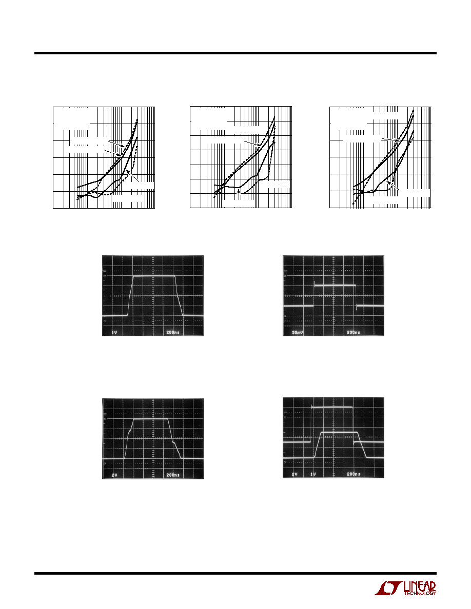
Amplifier Characteristics
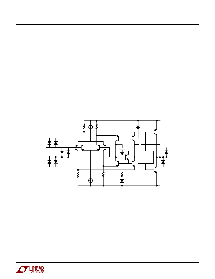
Figure 1 shows a simplified schematic of the LT6202/
LT6203/LT6204, which has two input differential amplifi-
ers in parallel that are biased on simultaneously when the
common mode voltage is at least 1.5V from either rail. This
topology allows the input stage to swing from the positive
supply voltage to the negative supply voltage. As the
common mode voltage swings beyond V
CC
≠ 1.5V, current
source I
1
saturates and current in Q1/Q4 is zero. Feedback
is maintained through the Q2/Q3 differential amplifier, but
with an input g
m
reduction of 1/2. A similar effect occurs
with I
2
when the common mode voltage swings within
1.5V of the negative rail. The effect of the g
m
reduction is
a shift in the V
OS
as I
1
or I
2
saturate.
Figure 1. Simplified Schematic
APPLICATIO S I FOR ATIO
W
U
U
U
Input bias current normally flows out of the + and ≠ inputs.
The magnitude of this current increases when the input
common mode voltage is within 1.5V of the negative rail,
and only Q1/Q4 are active. The polarity of this current
reverses when the input common mode voltage is within
1.5V of the positive rail and only Q2/Q3 are active.
The second stage is a folded cascode and current mirror
that converts the input stage differential signals to a single
ended output. Capacitor C1 reduces the unity cross
frequency and improves the frequency stability without
degrading the gain bandwidth of the amplifier. The
differential drive generator supplies current to the output
transistors that swing from rail-to-rail.
DIFFERENTIAL
DRIVE
GENERATOR
+
≠
R1
R2
R3
R4
R5
Q2
Q3
Q5
Q6
Q9
Q8
Q7
Q10
Q11
Q1
Q4
I
1
I
2
D3
D2
D1
DESD2
DESD4
DESD3
DESD1
DESD5
DESD6
+
≠
V
BIAS
C
M
C1
+V
+V
+V
+V
≠V
≠V
≠V
V
+
V≠
6203/04 F01
LT6202/LT6203/LT6204
16
620234fa
Input Protection
There are back-to-back diodes, D1 and D2, across the
+ and ≠ inputs of these amplifiers to limit the differential
input voltage to
±
0.7V. The inputs of the LT6202/LT6203/
LT6304 do not have internal resistors in series with the
input transistors. This technique is often used to protect
the input devices from over voltage that causes excessive
currents to flow. The addition of these resistors would
significantly degrade the low noise voltage of these ampli-
fiers. For instance, a 100
resistor in series with each
input would generate 1.8nV/
Hz of noise, and the total
amplifier noise voltage would rise from 1.9nV/
Hz to
2.6nV/
Hz. Once the input differential voltage exceeds
±
0.7V, steady state current conducted though the protec-
tion diodes should be limited to
±
40mA. This implies 25
of protection resistance per volt of continuous overdrive
beyond
±
0.7V. The input diodes are rugged enough to
handle transient currents due to amplifier slew rate over-
drive or momentary clipping without these resistors.
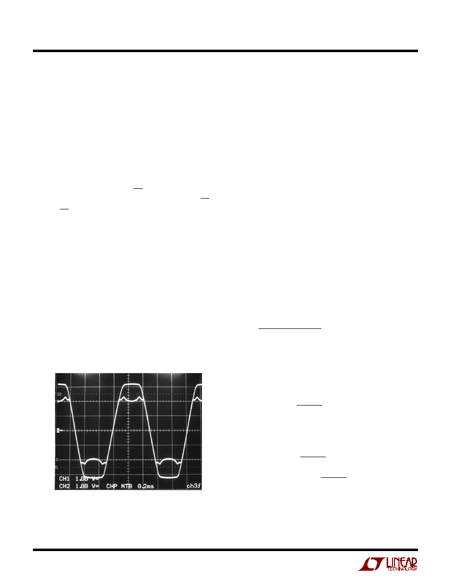
Figure 2 shows the input and output waveforms of the
amplifier driven into clipping while connected in a gain of
A
V
= 1. When the input signal goes sufficiently beyond the
power supply rails, the input transistors will saturate.
When saturation occurs, the amplifier loses a stage of
phase inversion and the output tries to change states.
Diodes D1 and D2 forward bias and hold the output within
a diode drop of the input signal. In this photo, the input
signal generator is clipping at
±
35mA, and the output
transistors supply this generator current through the
protection diodes.
With the amplifier connected in a gain of A
V
2, the output
can invert with very heavy input overdrive. To avoid this
inversion, limit the input overdrive to 0.5V beyond the
power supply rails.
ESD
The LT6202/LT6203/LT6204 have reverse-biased ESD
protection diodes on all inputs and outputs as shown in
Figure 1. If these pins are forced beyond either supply,
unlimited current will flow through these diodes. If the
current is transient and limited to one hundred milliamps
or less, no damage to the device will occur.
Noise
The noise voltage of the LT6202/LT6203/LT6204 is equiva-
lent to that of a 225
resistor, and for the lowest possible
noise it is desirable to keep the source and feedback
resistance at or below this value, i.e. R
S
+ R
G
||
R
FB
225
.
With R
S
+ R
G
||
R
FB
= 225
the total noise of the amplifier
is: e
n
=
(1.9nV)
2
+ (1.9nV)
2
= 2.7nV. Below this resistance
value, the amplifier dominates the noise, but in the resis-
tance region between 225
and approximately 10k
, the
noise is dominated by the resistor thermal noise. As the
total resistance is further increased, beyond 10k, the noise
current multiplied by the total resistance eventually domi-
nates the noise.
The product of e
n
∑
I
SUPPLY
is an interesting way to gauge
low noise amplifiers. Many low noise amplifiers with low
e
n
have high I
SUPPLY
current. In applications that require
low noise with the lowest possible supply current, this
product can prove to be enlightening. The LT6202/LT6203/
LT6204 have an e
n
,
I
SUPPLY
product of 3.2 per amplifier,
yet it is common to see amplifiers with similar noise
specifications have an e
n
∑
I
SUPPLY
product of 4.7 to 13.5.
For a complete discussion of amplifier noise, see the
LT1028 data sheet.
Figure 2. V
S
=
±
2.5V, A
V
= 1 with Large Overdrive
LT6202/03/04 F02
APPLICATIO S I FOR ATIO
W
U
U
U
OV

LT6202/LT6203/LT6204
17
620234fa
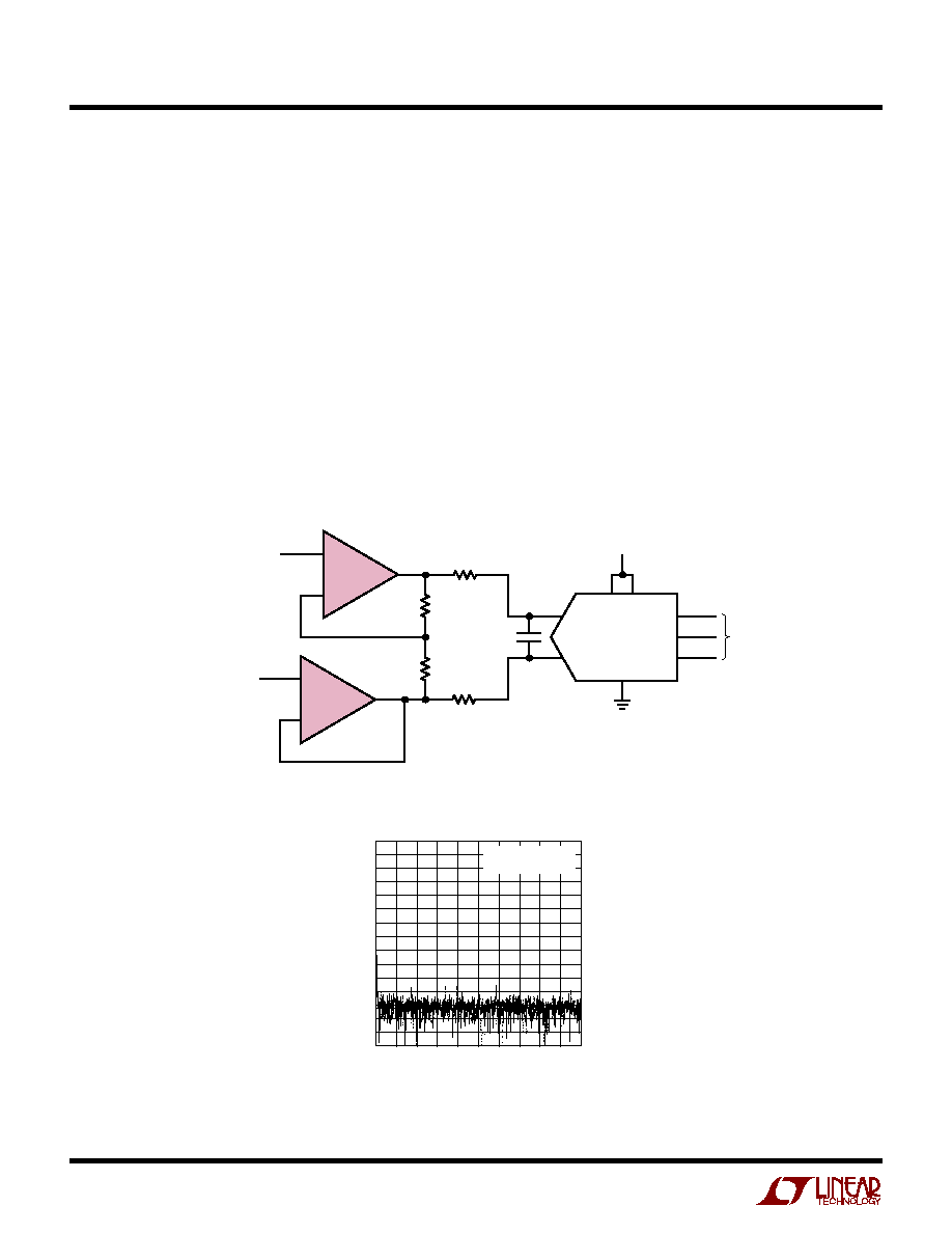
Low Noise, Low Power 1M
AC
Photodiode Transimpedance Amplifier
Figure 3 shows the LT6202 applied as a transimpedance
amplifier (TIA). The LT6202 forces the BF862 ultralow-
noise JFET source to 0V, with R3 ensuring that the JFET
has an I
DRAIN
of 1mA. The JFET acts as a source follower,
buffering the input of the LT6202 and making it suitable for
the high impedance feedback elements R1 and R2. The
BF862 has a minimum I
DSS
of 10mA and a pinchoff voltage
between ≠0.3V and ≠1.2V. The JFET gate and the LT6202
Figure 3. Low Noise, Low Power 1M
AC Photodiode Transimpedance Amplifier
Figure 4. Precision Low Noise, Low Power Transimpedance Amplifier
output therefore sit at a point slightly higher than one
pinchoff voltage below ground (typically about ≠0.6V).
When the photodiode is illuminated, the current must
come from the LT6202's output through R1 and R2, as in
a normal TIA. Amplifier input noise density and gain-
bandwidth product were measured at 2.4nV/Hz and
100MHz, respectively. Note that because the JFET has a
high g
m
, approximately 1/80
, its attenuation looking into
R3 is only about 2%. Gain-bandwidth product was mea-
sured at 100MHz and the closed-loop bandwidth using a
3pF photodiode was approximately 1.4MHz.
Precision Low Noise, Low Power, 1M
Photodiode Transimpedance Amplifier
Figure 4 shows the LT6202 applied as a transimpedance
amplifier (TIA), very similar to that shown in Figure 3. In
this case, however, the JFET is not allowed to dictate the
DC-bias conditions. Rather than being grounded, the
LT6202's noninverting input is driven by the LTC2050 to
the exact state necessary for zero JFET gate voltage. The
noise performance is nearly identical to that of the circuit
in Figure 3, with the additional benefit of excellent DC
performance. Input offset was measured at under 200
µ
V
and output noise was within 2mV
P-P
over a 20MHz
bandwidth.
≠
+
V
BIAS
≠
PHILIPS
BF862
R1
499k
R2
499k
C1
1pF
V
S
≠
V
S
+
V
OUT
V
S
=
±
5V
LT6202
R3
4.99k
LT6202/03/04 F03
≠
+
V
BIAS
≠
PHILIPS
BF862
R1
499k
R2
499k
C1
1pF
V
S
≠
V
S
+
V
OUT
V
S
=
±
5V
R3
4.99k
C2
0.1
µ
F
LTC2050HV
R4
10M
R5
10k
C3
1
µ
F
LT6202/03/04 F04
≠
+
LT6202
TYPICAL APPLICATIO S
U
LT6202/LT6203/LT6204
18
620234fa
Single-Supply 16-Bit ADC Driver
Figure 5 shows the LT6203 driving an LTC1864 unipolar
16-bit A/D converter. The bottom half of the LT6203 is in
a gain-of-one configuration and buffers the 0V negative
full-scale signal V
LOW
into the negative input of the
LTC1864. The top half of the LT6203 is in a gain-of-ten
configuration referenced to the buffered voltage V
LOW
and
drives the positive input of the LTC1864. The input range
of the LTC1864 is 0V to 5V, but for best results the input
range of V
IN
should be from V
LOW
(about 0.4V) to about
0.82V. Figure 6 shows an FFT obtained with a 10.1318kHz
coherent input waveform, from 8192 samples with no
windowing or averaging. Spurious free dynamic range is
seen to be about 100dB.
TYPICAL APPLICATIO S
U
Although the LTC1864 has a sample rate far below the gain
bandwidth of the LT6203, using this amplifier is not
necessarily a case of overkill. The designer is reminded
that A/D converters have sample apertures that are vanish-
ingly small (ideally, infinitesimally small) and make de-
mands on the upstream circuitry far in excess of what is
implied by the innocent-looking sample rate. In addition,
when an A/D converter takes a sample, it applies a small
capacitor to its inputs with a fair amount of glitch energy
and expects the voltage on the capacitor to settle to the
true value very quickly. Finally, the LTC1864 has a 20MHz
analog input bandwidth and can be used in undersampling
applications, again requiring a source bandwidth higher
than Nyquist.
≠
+
≠
+
≠
+
LTC1864
16-BIT
250ksps
5V
SERIAL
DATA
OUT
C1
470pF
R3
100
R4
100
R1
1k
R2
110
V
IN
= 0.6V
DC
±
200mV
AC
V
LOW
= 0.4V
DC
1/2 LT6203
1/2 LT6203
LT6202/03/04 F05
FREQUENCY (kHz)
0
SFDR (dB)
0
≠10
≠20
≠30
≠40
≠50
≠60
≠70
≠80
≠90
≠100
≠110
≠120
≠130
≠140
≠150
37.5
62.5
100
LT6202/03/04 F06
12.5 25
50
75 82.5
112.5 125
f
S
= 250ksps
f
IN
= 10.131836kHz
Figure 5. Single-Supply 16-Bit ADC Driver
Figure 6. FFT Showing 100dB SFDR
LT6202/LT6203/LT6204
19
620234fa
PACKAGE DESCRIPTIO
U
GN16 (SSOP) 0502
1
2
3
4
5
6
7
8
.229 ≠ .244
(5.817 ≠ 6.198)
.150 ≠ .157**
(3.810 ≠ 3.988)
16 15 14 13
.189 ≠ .196*
(4.801 ≠ 4.978)
12 11 10 9
.016 ≠ .050
(0.406 ≠ 1.270)
.015
±
.004
(0.38
±
0.10)
◊
45
∞
0
∞
≠ 8
∞
TYP
.007 ≠ .0098
(0.178 ≠ 0.249)
.053 ≠ .068
(1.351 ≠ 1.727)
.008 ≠ .012
(0.203 ≠ 0.305)
.004 ≠ .0098
(0.102 ≠ 0.249)
.0250
(0.635)
BSC
.009
(0.229)
REF
.254 MIN
RECOMMENDED SOLDER PAD LAYOUT
.150 ≠ .165
.0250 TYP
.0165
±
.0015
.045
±
.005
*DIMENSION DOES NOT INCLUDE MOLD FLASH. MOLD FLASH
SHALL NOT EXCEED 0.006" (0.152mm) PER SIDE
**DIMENSION DOES NOT INCLUDE INTERLEAD FLASH. INTERLEAD
FLASH SHALL NOT EXCEED 0.010" (0.254mm) PER SIDE
INCHES
(MILLIMETERS)
NOTE:
1. CONTROLLING DIMENSION: INCHES
2. DIMENSIONS ARE IN
3. DRAWING NOT TO SCALE
GN Package
16-Lead Plastic SSOP (Narrow .150 Inch)
(Reference LTC DWG # 05-08-1641)
DD Package
8-Lead Plastic DFN (3mm
◊
3mm)
(Reference LTC DWG # 05-08-1698)
3.00
±
0.10
(4 SIDES)
NOTE:
1. DRAWING TO BE MADE A JEDEC PACKAGE OUTLINE M0-229 VARIATION OF (WEED-1)
2. ALL DIMENSIONS ARE IN MILLIMETERS
3. DIMENSIONS OF EXPOSED PAD ON BOTTOM OF PACKAGE DO NOT INCLUDE
MOLD FLASH. MOLD FLASH, IF PRESENT, SHALL NOT EXCEED 0.15mm ON ANY SIDE
4. EXPOSED PAD SHALL BE SOLDER PLATED
0.38
±
0.10
BOTTOM VIEW--EXPOSED PAD
1.65
±
0.10
(2 SIDES)
0.75
±
0.05
R = 0.115
TYP
2.38
±
0.10
(2 SIDES)
1
4
8
5
PIN 1
TOP MARK
0.200 REF
0.00 ≠ 0.05
(DD8) DFN 0203
0.28
±
0.05
2.38
±
0.05
(2 SIDES)
RECOMMENDED SOLDER PAD PITCH AND DIMENSIONS
1.65
±
0.05
(2 SIDES)
2.15
±
0.05
0.50
BSC
0.675
±
0.05
3.5
±
0.05
PACKAGE
OUTLINE
0.28
±
0.05
0.50 BSC
LT6202/LT6203/LT6204
20
620234fa
PACKAGE DESCRIPTIO
U
MS8 Package
8-Lead Plastic MSOP
(Reference LTC DWG # 05-08-1660)
MSOP (MS8) 0802
0.53
±
0.015
(.021
±
.006)
SEATING
PLANE
NOTE:
1. DIMENSIONS IN MILLIMETER/(INCH)
2. DRAWING NOT TO SCALE
3. DIMENSION DOES NOT INCLUDE MOLD FLASH, PROTRUSIONS OR GATE BURRS.
MOLD FLASH, PROTRUSIONS OR GATE BURRS SHALL NOT EXCEED 0.152mm (.006") PER SIDE
4. DIMENSION DOES NOT INCLUDE INTERLEAD FLASH OR PROTRUSIONS.
INTERLEAD FLASH OR PROTRUSIONS SHALL NOT EXCEED 0.152mm (.006") PER SIDE
5. LEAD COPLANARITY (BOTTOM OF LEADS AFTER FORMING) SHALL BE 0.102mm (.004") MAX
0.18
(.077)
0.254
(.010)
1.10
(.043)
MAX
0.22 ≠ 0.38
(.009 ≠ .015)
TYP
0.13
±
0.076
(.005
±
.003)
0.86
(.034)
REF
0.65
(.0256)
BSC
0
∞
≠ 6
∞
TYP
DETAIL "A"
DETAIL "A"
GAUGE PLANE
1
2
3
4
4.90
±
0.15
(1.93
±
.006)
8
7 6 5
3.00
±
0.102
(.118
±
.004)
(NOTE 3)
3.00
±
0.102
(.118
±
.004)
NOTE 4
0.52
(.206)
REF
5.23
(.206)
MIN
3.2 ≠ 3.45
(.126 ≠ .136)
0.889
±
0.127
(.035
±
.005)
RECOMMENDED SOLDER PAD LAYOUT
0.42
±
0.04
(.0165
±
.0015)
TYP
0.65
(.0256)
BSC
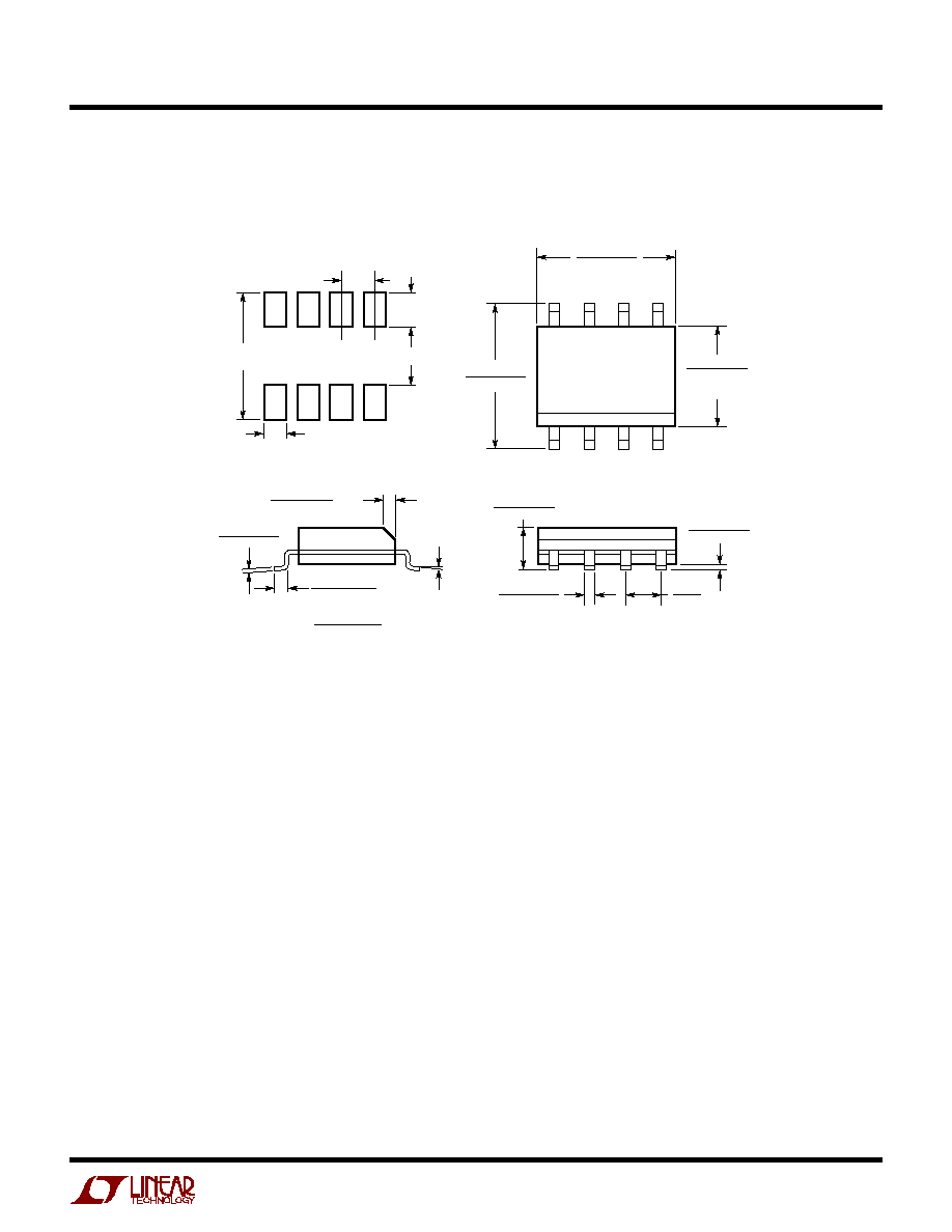
LT6202/LT6203/LT6204
21
620234fa
PACKAGE DESCRIPTIO
U
S8 Package
8-Lead Plastic Small Outline (Narrow .150 Inch)
(Reference LTC DWG # 05-08-1610)
.016 ≠ .050
(0.406 ≠ 1.270)
.010 ≠ .020
(0.254 ≠ 0.508)
◊
45
∞
0
∞
≠ 8
∞
TYP
.008 ≠ .010
(0.203 ≠ 0.254)
SO8 0303
.053 ≠ .069
(1.346 ≠ 1.752)
.014 ≠ .019
(0.355 ≠ 0.483)
TYP
.004 ≠ .010
(0.101 ≠ 0.254)
.050
(1.270)
BSC
1
2
3
4
.150 ≠ .157
(3.810 ≠ 3.988)
NOTE 3
8
7
6
5
.189 ≠ .197
(4.801 ≠ 5.004)
NOTE 3
.228 ≠ .244
(5.791 ≠ 6.197)
.245
MIN
.160
±
.005
RECOMMENDED SOLDER PAD LAYOUT
.045
±
.005
.050 BSC
.030
±
.005
TYP
INCHES
(MILLIMETERS)
NOTE:
1. DIMENSIONS IN
2. DRAWING NOT TO SCALE
3. THESE DIMENSIONS DO NOT INCLUDE MOLD FLASH OR PROTRUSIONS.
MOLD FLASH OR PROTRUSIONS SHALL NOT EXCEED .006" (0.15mm)

LT6202/LT6203/LT6204
22
620234fa
PACKAGE DESCRIPTIO
U
S Package
14-Lead Plastic Small Outline (Narrow .150 Inch)
(Reference LTC DWG # 05-08-1610)
1
N
2
3
4
.150 ≠ .157
(3.810 ≠ 3.988)
NOTE 3
14
13
.337 ≠ .344
(8.560 ≠ 8.738)
NOTE 3
.228 ≠ .244
(5.791 ≠ 6.197)
12
11
10
9
5
6
7
N/2
8
.016 ≠ .050
(0.406 ≠ 1.270)
.010 ≠ .020
(0.254 ≠ 0.508)
◊
45
∞
0
∞
≠ 8
∞
TYP
.008 ≠ .010
(0.203 ≠ 0.254)
S14 0502
.053 ≠ .069
(1.346 ≠ 1.752)
.014 ≠ .019
(0.355 ≠ 0.483)
TYP
.004 ≠ .010
(0.101 ≠ 0.254)
.050
(1.270)
BSC
.245
MIN
N
1
2
3
N/2
.160
±
.005
RECOMMENDED SOLDER PAD LAYOUT
.045
±
.005
.050 BSC
.030
±
.005
TYP
INCHES
(MILLIMETERS)
NOTE:
1. DIMENSIONS IN
2. DRAWING NOT TO SCALE
3. THESE DIMENSIONS DO NOT INCLUDE MOLD FLASH OR PROTRUSIONS.
MOLD FLASH OR PROTRUSIONS SHALL NOT EXCEED .006" (0.15mm)
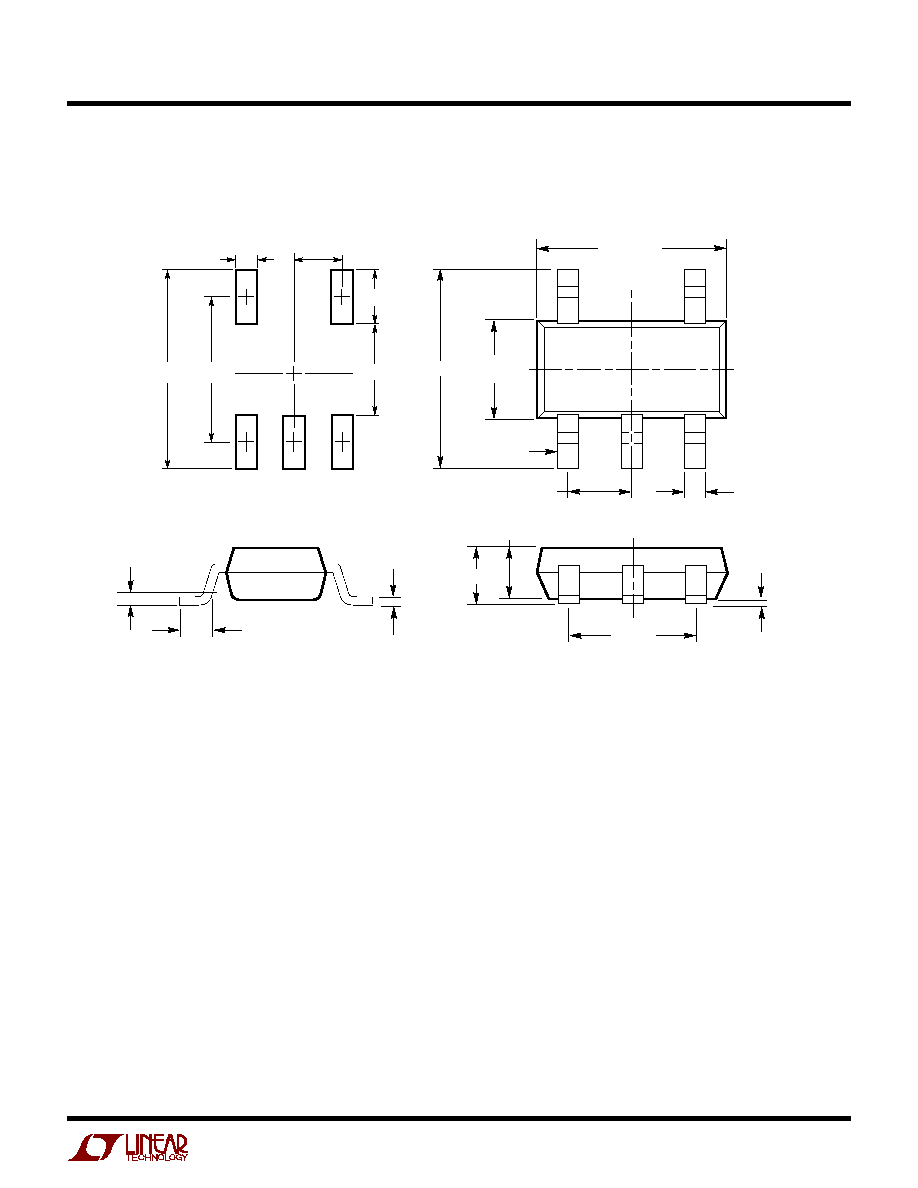
LT6202/LT6203/LT6204
23
620234fa
PACKAGE DESCRIPTIO
U
S5 Package
5-Lead Plastic TSOT-23
(Reference LTC DWG # 05-08-1635)
1.50 ≠ 1.75
(NOTE 4)
2.80 BSC
0.30 ≠ 0.45 TYP
5 PLCS (NOTE 3)
DATUM `A'
0.09 ≠ 0.20
(NOTE 3)
S5 TSOT-23 0302
PIN ONE
2.90 BSC
(NOTE 4)
0.95 BSC
1.90 BSC
0.80 ≠ 0.90
1.00 MAX
0.01 ≠ 0.10
0.20 BSC
0.30 ≠ 0.50 REF
NOTE:
1. DIMENSIONS ARE IN MILLIMETERS
2. DRAWING NOT TO SCALE
3. DIMENSIONS ARE INCLUSIVE OF PLATING
4. DIMENSIONS ARE EXCLUSIVE OF MOLD FLASH AND METAL BURR
5. MOLD FLASH SHALL NOT EXCEED 0.254mm
6. JEDEC PACKAGE REFERENCE IS MO-193
3.85 MAX
0.62
MAX
0.95
REF
RECOMMENDED SOLDER PAD LAYOUT
PER IPC CALCULATOR
1.4 MIN
2.62 REF
1.22 REF
Information furnished by Linear Technology Corporation is believed to be accurate and reliable.
However, no responsibility is assumed for its use. Linear Technology Corporation makes no represen-
tation that the interconnection of its circuits as described herein will not infringe on existing patent rights.
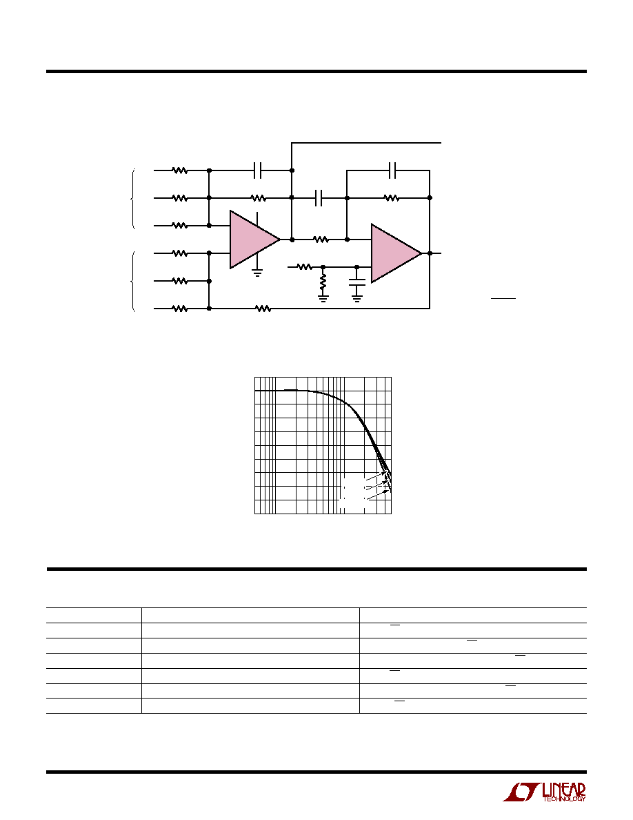
LT6202/LT6203/LT6204
24
620234fa
Linear Technology Corporation
1630 McCarthy Blvd., Milpitas, CA 95035-7417
(408) 432-1900
q
FAX: (408) 434-0507
q
www.linear.com
©
LINEAR TECHNOLOGY CORPORATION 2002
LT/TP 0403 1K ∑ PRINTED IN USA
RELATED PARTS
TYPICAL APPLICATIO
U
PART NUMBER
DESCRIPTION
COMMENTS
LT1028
Single, Ultralow Noise 50MHz Op Amp
1.1nV/
Hz
LT1677
Single, Low Noise Rail-to-Rail Amplifier
3V Operation, 2.5mA, 4.5nV/
Hz, 60
µ
V Max V
0S
LT1722/LT1723/LT1724
Single/Dual/Quad Low Noise Precision Op Amps
70V/
µ
s Slew Rate, 400
µ
V Max V
OS
, 3.8nV/
Hz, 3.7mA
LT1800/LT1801/LT1802
Single/Dual/Quad Low Power 80MHz Rail-to-Rail Op Amps
8.5nV/
Hz, 2mA Max Supply
LT1806/LT1807
Single/Dual, Low Noise 325MHz Rail-to-Rail Amplifiers
2.5V Operation, 550
µ
V Max V
OS
, 3.5nV/
Hz
LT6200
Single Ultralow Noise Rail-to-Rail Amplifier
0.95nV/
Hz, 165MHz Gain Bandwidth
≠
+
≠
+
R1
402
R2
200
R3
100
R4
402
R5
200
R6
100
0dB
6dB
12dB
0dB
6dB
12dB
1/2 LT6203
1/2 LT6203
C1
270pF
R7, 402
R9
402
R
A
R
B
V
+
0.1
µ
F
R8
402
C2
22pF
V
+
C3
5pF
R10, 402
V
OUT
+
V
OUT
≠
V
IN
≠
V
IN
+
LT6202/03/04 F07
R
B
R
A
+ R
B
OUTPUT V
CM
=
V
+
( )
FREQUENCY (Hz)
50k
RELATIVE DIFFERENTIAL GAIN (1dB/DIV)
1M
5M
LT6202/03/04 F08
G = 6dB
G = 12dB
G = 0dB
Low Noise Differential Amplifier with Gain Adjust and Common Mode Control
Low Noise Differential Amplifier
Frequency Response