 | ÐлекÑÑоннÑй компоненÑ: LT6207 | СкаÑаÑÑ:  PDF PDF  ZIP ZIP |
Äîêóìåíòàöèÿ è îïèñàíèÿ www.docs.chipfind.ru
LT6205/LT6206/LT6207
1
620567f
APPLICATIO S
U
FEATURES
TYPICAL APPLICATIO
U
DESCRIPTIO
U
s
450V/
µ
s Slew Rate
s
100MHz Gain Bandwidth Product
s
Wide Supply Range 2.7V to 12.6V
s
Output Swings Rail-to-Rail
s
Input Common Mode Range Includes Ground
s
High Output Drive: 50mA
s
Channel Separation: 90dB at 10MHz
s
Specified on 3V, 5V, and
±
5V Supplies
s
Input Offset Voltage: 1mV
s
Low Power Dissipation: 20mW Per Amplifier on
Single 5V
s
Operating Temperature Range: 40
°
C to 85
°
C
s
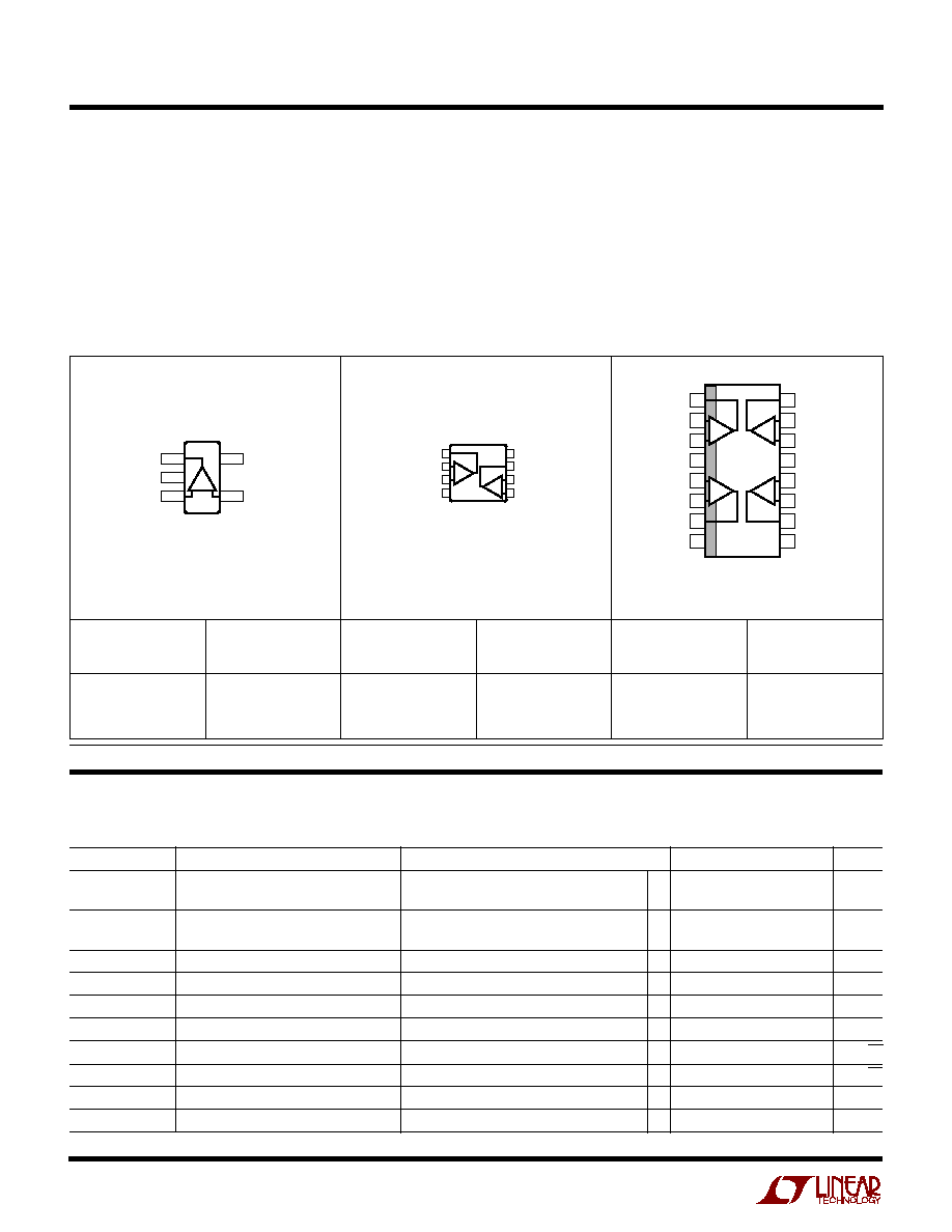
Single in SOT-23, Dual in MSOP,
Quad in SSOP Package
Single/Dual/Quad
Single Supply 3V,
100MHz Video Op Amps
The LT
®
6205/LT6206/LT6207 are low cost single/dual/
quad voltage feedback amplifiers that feature 100MHz
gain-bandwidth product, 450V/
µ
s slew rate and 50mA
output current. These amplifiers have an input range that
includes ground and an output that swings within 60mV of
either supply rail, making them well suited for single
supply operation.
These amplifiers maintain their performance for supplies
from 2.7V to 12.6V and are specified at 3V, 5V and
±
5V.
The inputs can be driven beyond the supplies without
damage or phase reversal of the output. Isolation between
channels is high, over 90dB at 10MHz.
The LT6205 is available in the 5-pin SOT-23, and the
LT6206 is available in an 8-lead MSOP package with
standard op amp pin-outs. For compact layouts the quad
LT6207 is available in the 16-pin SSOP package. These
devices are specified over the commercial and industrial
temperature ranges.
, LTC and LT are registered trademarks of Linear Technology Corporation.
s
Video Line Driver
s
Automotive Displays
s
RGB Amplifiers
s
Coaxial Cable Drivers
s
Low Voltage High Speed Signal Processing
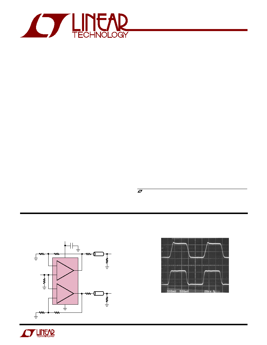
+
+
LT6206
V
IN
1
µ
F
75
75
75
75
75
V
OUT1
V
OUT2
3.3V
499
499
499
499
1
7
4
8
6
5
3
2
F
3dB
50MHz
I
S
25mA
620567 TA01a
Baseband Video Splitter/Cable Driver
V
IN
V
OUT
20ns/DIV
V
S
= 3.3V
V
IN
= 0.1V TO 1.1V
f = 10MHz
0V
0V
620567 TA01b
Output Step Response
LT6205/LT6206/LT6207
2
620567f
Total Supply Voltage (V
+
to V
) ............................ 12.6V
Input Current ......................................................
±
10mA
Input Voltage Range (Note 2) ...................................
±
V
S
Output Short-Circuit Duration (Note 3) ............ Indefinite
Pin Current While Exceeding Supplies (Note 9) ..
±
25mA
MS8 PART
MARKING
T
JMAX
= 150
°
C,
JA
= 250
°
C/W
LTH3
LTH4
ABSOLUTE AXI U
RATI GS
W
W
W
U
PACKAGE/ORDER I FOR ATIO
U
U
W
(Note 1)
ELECTRICAL CHARACTERISTICS
The
q
denotes specifications which apply over the specified temperature
range, otherwise specifications are at T
A
= 25
°
C. V
S
= 3V, 0V; V
S
= 5V, 0V; V
CM
= V
OUT
= 1V, unless otherwise noted.
SYMBOL
PARAMETER
CONDITIONS
MIN
TYP
MAX
UNITS
V
OS
Input Offset Voltage
1
3.5
mV
q
5
mV
Input Offset Voltage Match
1
3
mV
(Channel-to-Channel) (Note 5)
q
4
mV
Input Offset Voltage Drift (Note 6)
q
7
15
µ
V/
°
C
I
B
Input Bias Current
q
10
30
µ
A
I
OS
Input Offset Current
q
0.6
3
µ
A
Input Noise Voltage
0.1Hz to 10Hz
2
µ
V
P-P
e
n
Input Noise Voltage Density
f = 10kHz
9
nV/
Hz
i
n
Input Noise Current Density
f = 10kHz
4
pA/
Hz
Input Resistance
V
CM
= 0V to V
+
2V
1
M
Input Capacitance
2
pF
*The temperature grades are identified by a label on the shipping container. Consult LTC Marketing for parts specified with wider operating temperature ranges.
1
2
3
4
OUT A
IN A
+IN A
V
8
7
6
5
V
+
OUT B
IN B
+IN B
TOP VIEW
MS8 PACKAGE
8-LEAD PLASTIC MSOP
+
+
Operating Temperature Range .................40
°
C to 85
°
C
Specified Temperature Range (Note 4) ....40
°
C to 85
°
C
Storage Temperature Range ..................65
°
C to 150
°
C
Maximum Junction Temperature .......................... 150
°
C
Lead Temperature (Soldering, 10 sec).................. 300
°
C
ORDER PART
NUMBER
LT6206CMS8
LT6206IMS8
S5 PART
MARKING*
LTAEM
ORDER PART
NUMBER
LT6205CS5
LT6205IS5
GN PART
MARKING
6207
6207I
ORDER PART
NUMBER
LT6207CGN
LT6207IGN
TOP VIEW
GN PACKAGE
16-LEAD NARROW PLASTIC SSOP
1
2
3
4
5
6
7
8
16
15
14
13
12
11
10
9
OUT A
IN A
+IN A
V
+
+IN B
IN B
OUT B
NC
OUT D
IN D
+IN D
V
+IN C
IN C
OUT C
NC
C
+
D
+
B
+
A
+
5 V
+
4 IN
OUT 1
TOP VIEW
S5 PACKAGE
5-LEAD PLASTIC SOT-23
V
2
+IN 3
+
T
JMAX
= 150
°
C,
JA
= 135
°
C/W
T
JMAX
= 150
°
C,
JA
= 250
°
C/W
LT6205/LT6206/LT6207
3
620567f
ELECTRICAL CHARACTERISTICS
The
q
denotes specifications which apply over the specified temperature
range, otherwise specifications are at T
A
= 25
°
C. V
S
= 3V, 0V; V
S
= 5V, 0V; V
CM
= V
OUT
= 1V, unless otherwise noted.
SYMBOL
PARAMETER
CONDITIONS
MIN
TYP
MAX
UNITS
CMRR
Common Mode Rejection Ratio
V
CM
= 0 to V
+
2V
q
78
90
dB
Input Voltage Range
q
0
V
+
2
V
PSRR
Power Supply Rejection Ratio
V
S
= 3V to 12V
q
67
75
dB
V
CM
= V
OUT
= 0.5V
Minimum Supply Voltage
V
CM
= 0.5V
q
2.7
V
A
VOL
Large-Signal Voltage Gain
V
S
= 5V, V
O
= 0.5V to 4.5V, R
L
= 1k
q
30
100
V/mV
V
S
= 5V, V
O
= 1V to 3V, R
L
= 150
q
5
20
V/mV
V
S
= 3V, V
O
= 0.5V to 2.5V, R
L
= 1k
q
20
60
V/mV
V
OL
Output Voltage Swing Low (Note 7)
No Load, Input Overdrive = 30mV
q
10
25
mV
I
SINK
= 5mA
q
75
150
mV
V
S
= 5V, I
SINK
= 25mA
q
300
500
mV
V
S
= 3V, I
SINK
= 15mA
q
200
350
mV
V
OH
Output Voltage Swing High (Note 7)
No Load, Input Overdrive = 30mV
q
60
100
mV
I
SOURCE
= 5mA
q
140
250
mV
V
S
= 5V, I
SOURCE
= 25mA
q
650
1200
mV
V
S
= 3V, I
SOURCE
= 15mA
q
300
500
mV
I
SC
Short-Circuit Current
V
S
= 5V, Output Shorted to GND
35
60
mA
q
25
mA
V
S
= 3V, Output Shorted to GND
30
50
mA
q
20
mA
I
S
Supply Current per Amplifier
3.75
5
mA
q
5.75
mA
GBW
Gain Bandwidth Product
f = 2MHz
q
65
100
MHz
SR
Slew Rate
V
S
= 5V, A
V
= 2, R
F
= R
G
= 1k
450
V/
µ
s
V
O
= 1V to 4V, Measured from 1.5V to 3.5V
Channel Separation
f = 10MHz
90
dB
FPBW
Full Power Bandwidth
V
OUT
= 2V
P-P
(Note 8)
71
MHz
t
S
Settling time to 3%
V
S
= 5V,
V
OUT
= 2V, A
V
= 1, R
L
= 150
15
ns
Settling time to 1%
25
ns
Differential Gain
V
S
= 5V, A
V
= 2, R
L
= 150
, Output Black Level =1V
0.05
%
Differential Phase
V
S
= 5V, A
V
= 2, R
L
= 150
, Output Black Level =1V
0.08
Deg
The
q
denotes specifications which apply over the specified temperature range, otherwise specifications are at T
A
= 25
°
C. V
S
=
±
5V;
V
CM
= V
OUT
= 0V, unless otherwise noted.
SYMBOL
PARAMETER
CONDITIONS
MIN
TYP
MAX
UNITS
V
OS
Input Offset Voltage
1.3
4.5
mV
q
6
mV
Input Offset Voltage Match
1
3
mV
(Channel-to-Channel) (Note 5)
q
4
mV
Input Offset Voltage Drift (Note 6)
q
10
18
µ
V/
°
C
I
B
Input Bias Current
q
18
30
µ
A
I
OS
Input Offset Current
q
0.6
3
µ
A
Input Noise Voltage
0.1Hz to 10Hz
2
µ
V
P-P
LT6205/LT6206/LT6207
4
620567f
SYMBOL
PARAMETER
CONDITIONS
MIN
TYP
MAX
UNITS
e
n
Input Noise Voltage Density
f = 10kHz
9
nV/
Hz
i
n
Input Noise Current Density
f = 10kHz
4
pA/
Hz
Input Resistance
V
CM
= 5V to 3V
1
M
Input Capacitance
2
pF
CMRR
Common Mode Rejection Ratio
V
CM
= 5V to 3V
q
78
90
dB
Input Voltage Range
q
5
3
V
PSRR
Power Supply Rejection Ratio
V
S
=
±
2V to
±
6V
q
67
75
dB
A
VOL
Large-Signal Voltage Gain
V
O
= 4V to 4V, R
L
= 1k
q
50
133
V/mV
V
O
= 3V to 3V, R
L
= 150
q
7.5
20
V/mV
Output Voltage Swing
No Load, Input Overdrive = 30mV
q
±
4.88
±
4.92
V
I
OUT
=
±
5mA
q
±
4.75
±
4.85
V
I
OUT
=
±
25mA
q
±
3.8
±
4.35
V
I
SC
Short-Circuit Current
Short to Ground
±
40
±
60
mA
q
±
30
mA
I
S
Supply Current per Amplifier
4
5.6
mA
q
6.5
mA
GBW
Gain Bandwidth Product
f = 2MHz
q
65
100
MHz
SR
Slew Rate
A
V
= 1, R
L
= 1k
350
600
V/
µ
s
V
O
= 4V to 4V, Measured from 3V to 3V
Channel Separation
f = 10MHz
90
dB
FPBW
Full Power Bandwidth
V
OUT
= 8V
P-P
(Note 8)
14
24
MHz
t
S
Settling Time to 3%
V
OUT
= 2V, A
V
= 1, R
L
= 150
15
ns
Settling Time to 1%
25
ns
Differential Gain
A
V
= 2, R
L
= 150
, Output Black Level = 1V
0.05
%
Differential Phase
A
V
= 2, R
L
= 150
, Output Black Level = 1V
0.08
Deg
ELECTRICAL CHARACTERISTICS
The
q
denotes specifications which apply over the specified temperature
range, otherwise specifications are at T
A
= 25
°
C. V
S
=
±
5V; V
CM
= V
OUT
= 0V, unless otherwise noted.
Note 1: Absolute Maximum ratings are those values beyond which the life
of a device may be impaired.
Note 2: The inputs are protected by back-to-back diodes. If the differential
input voltage exceeds 1.4V, the input current should be limited to less than
10mA.
Note 3: A heat sink may be required to keep the junction temperature
below absolute maximum. This depends on the power supply voltage and
how many amplifiers are shorted.
Note 4: The LT6205C/LT6206C/LT6207C are guaranteed to meet specified
performance from 0
°
C to 70
°
C and are designed, characterized and
expected to meet specified performance from 40
°
C to 85
°
C but are not
tested or QA sampled at these temperatures. The LT6205I/LT6206I/
LT6207I are guaranteed to meet specified performance from
40
°
C to 85
°
C.
Note 5: Matching parameters are the difference between the two amplifiers
A and D and between B and C of the LT6207; between the two amplifiers
of the LT6206.
Note 6: This parameter is not 100% tested.
Note 7: Output voltage swings are measured between the output and
power supply rails.
Note 8: Full power bandwidth is calculated from the slew rate
measurement: FPBW = SR/2
V
PEAK
.
Note 9: There are reverse biased ESD diodes on all inputs and outputs.
If these pins are forced beyond either supply, unlimited current will flow
through these diodes. If the current is transient in nature and limited to
less than 25mA, no damage to the device will occur.
LT6205/LT6206/LT6207
5
620567f
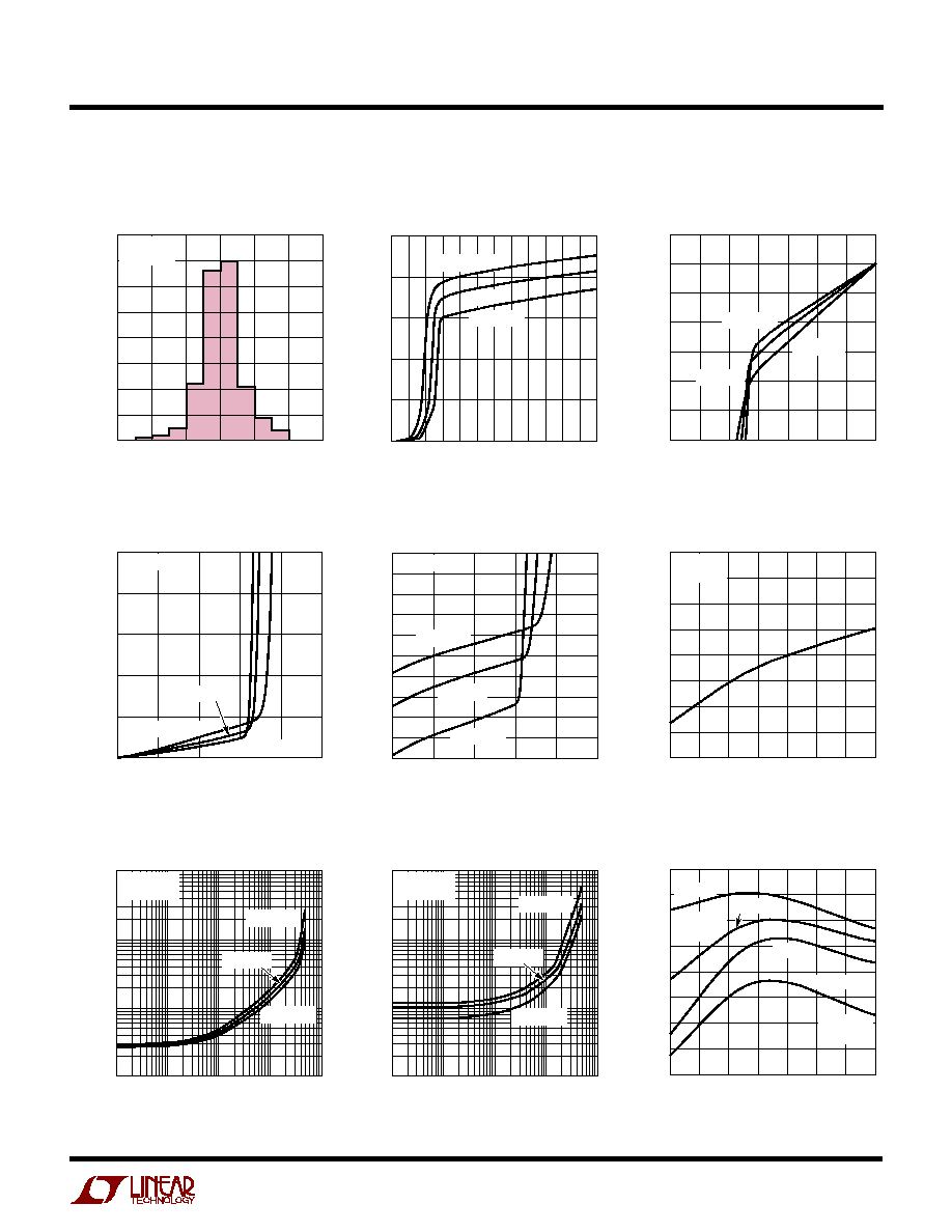
TOTAL SUPPLY VOLTAGE (V)
1.5
2.0
2.5
3.0
3.5
4.0
4.5
5.0
CHANGE IN INPUT OFFSET VOLTAGE (
µ
V)
620567 G03
100
0
100
200
300
400
500
600
T
A
= 25
°
C
T
A
= 55
°
C
T
A
=125
°
C
V
OS
Distribution
Supply Current per Amplifier vs
Supply Voltage
Minimum Supply Voltage
Change in Offset Voltage vs Input
Common Mode Voltage
Input Bias Current vs Input
Common Mode Voltage
Input Bias Current vs
Temperature
Output Saturation Voltage vs
Load Current (Output Low)
Output Saturation Voltage vs
Load Current (Output High)
Short-Circuit Current vs
Temperature
TYPICAL PERFOR A CE CHARACTERISTICS
U
W
TEMPERATURE (
°
C)
50
25
0
25
50
75
100
125
INPUT BIAS CURRENT (
µ
A)
620567 G06
4
6
5
7
8
9
10
11
12
V
S
= 5V, 0V
V
CM
= 1V
TOTAL SUPPLY VOLTAGE (V)
0
1
2
3
4
5
6
7
8
9 10 11 12
SUPPLY CURRENT PER AMPLIFIER (mA)
620567 G02
5
4
3
2
1
0
T
A
= 25
°
C
T
A
= 55
°
C
T
A
= 125
°
C
INPUT COMMON MODE VOLTAGE (V)
0
1
2
3
4
5
INPUT BIAS CURRENT (
µ
A)
2
3
4
5
6
7
9
12
8
11
10
V
S
= 5V, 0V
T
A
= 25
°
C
T
A
= 55
°
C
T
A
= 125
°
C
620567 G05
LOAD CURRENT (mA)
0.1
OUTPUT SATURATION VOLTAGE (V)
1
0.01
1
10
100
620567 G07
0.01
0.1
10
V
S
= 5V, 0V
V
OD
= 30mV
T
A
= 25
°
C
T
A
= 55
°
C
T
A
= 125
°
C
LOAD CURRENT (mA)
0.1
OUTPUT SATURATION VOLTAGE (V)
1
0.01
1
10
100
620567 G08
0.01
0.1
10
T
A
= 25
°
C
T
A
= 55
°
C
T
A
= 125
°
C
V
S
= 5V, 0V
V
OD
= 30mV
TEMPERATURE (
°
C)
50
25
0
25
50
75
100
125
OUTPUT SHORT-CIRCUIT CURRENT (mA)
620567 G09
75
65
70
60
55
50
45
40
35
V
S
= 5V, 0V
V
CM
= 1V
V
S
= 3V, 0V
V
CM
= 1V
SINKING
SOURCING
SINKING
SOURCING
INPUT OFFSET VOLTAGE (mV)
3
2
1
0
1
2
3
PERCENT OF UNITS (%)
620567 G01
40
30
35
25
20
15
10
5
0
V
S
= 5V, 0V
V
CM
= 1V
INPUT COMMON MODE VOLTAGE (V)
0
1
2
3
4
5
OFFSET VOLTAGE CHANGE (
µ
V)
620567 G04
1000
800
600
400
200
0
T
A
= 25
°
C
T
A
= 55
°
C
T
A
=125
°
C
V
S
= 5V, 0V