 | ÐлекÑÑоннÑй компоненÑ: LT6230 | СкаÑаÑÑ:  PDF PDF  ZIP ZIP |
Äîêóìåíòàöèÿ è îïèñàíèÿ www.docs.chipfind.ru
1
sn623012 623012fas
LT6230/LT6230-10/
LT6231/LT6232
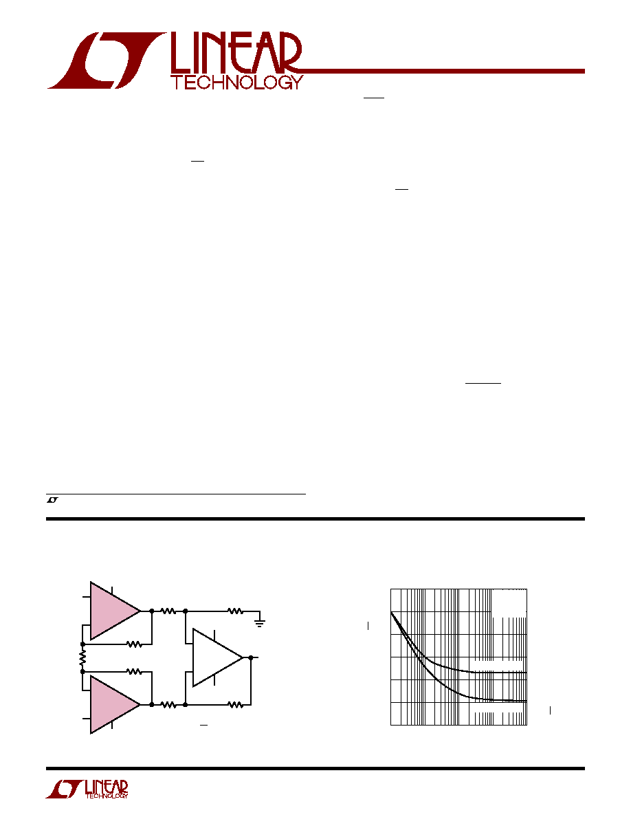
+
R6
499
LT6202
V
S
+
V
OUT
IN
+
IN
+
1/2 LT6231
V
S
V
S
+
+
1/2 LT6231
R7
499
R4
499
R2
196
R1
10
R3
196
R5
499
623012 TA01a
A
V
= 40
BW = 5.1MHz
V
S
=
±
1.5V to
±
5V
I
S
= 10mA
E
N
= 5.8
µ
V
RMS
INPUT REFERRED,
MEASUREMENT BW = 8MHz
V
S
s
Ultrasound Amplifiers
s
Low Noise, Low Power Signal Processing
s
Active Filters
s
Driving A/D Converters
s
Rail-to-Rail Buffer Amplifiers
s
Low Noise Voltage: 1.1nV/
Hz
s
Low Supply Current: 3.5mA/Amp Max
s
Low Offset Voltage: 350
µ
V Max
s
Gain Bandwidth Product:
LT6230: 215MHz; A
V
1
LT6230-10: 1450MHz; A
V
10
s
Wide Supply Range: 3V to 12.6V
s
Output Swings Rail-to-Rail
s
Common Mode Rejection Ratio 115dB Typ
s
Output Current: 30mA
s
Operating Temperature Range 40
°
C to 85
°
C
s
LT6230 Shutdown to 10
µ
A Maximum
s
LT6230/LT6230-10 in SOT-23 Package
s
Dual LT6231 in 8-Pin SO and Tiny DFN Packages
s
LT6232 in 16-Pin SSOP Package
APPLICATIO S
U
FEATURES
TYPICAL APPLICATIO
U
DESCRIPTIO
U
215MHz, Rail-to-Rail Output,
1.1nV/
Hz, 3.5mA Op Amp Family
, LTC and LT are registered trademarks of Linear Technology Corporation.
The LT
®
6230/LT6231/LT6232 are single/dual/quad low
noise, rail-to-rail output unity gain stable op amps that
feature 1.1nV/
Hz noise voltage and draw only 3.5mA of
supply current per amplifier. These amplifiers combine
very low noise and supply current with a 215MHz gain
bandwidth product, a 70V/
µ
s slew rate and are optimized
for low supply voltage signal conditioning systems. The
LT6230-10 is a single amplifier optimized for higher gain
applications resulting in higher gain bandwidth and slew
rate. The LT6230 and LT6230-10 include an enable pin
that can be used to reduce the supply current to less than
10
µ
A.
The amplifier family has an output that swings within
50mV of either supply rail to maximize the signal dynamic
range in low supply applications and is specified on 3.3V,
5V and
±
5V supplies. The e
n
·
I
SUPPLY
product of 1.9 per
amplifier is among the most noise efficient of any op amp.
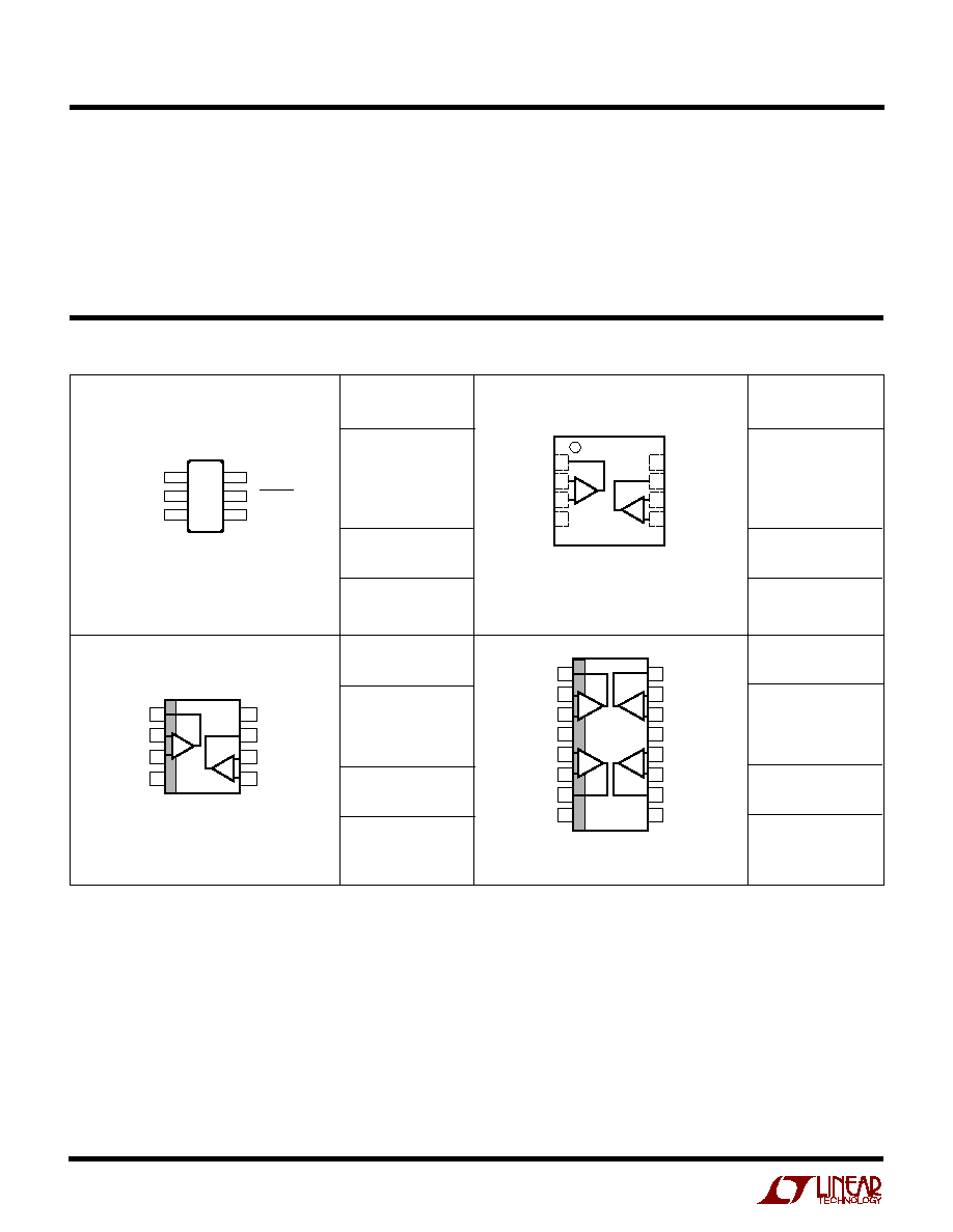
The LT6230/LT6230-10 is available in the 6-lead SOT-23
package and the LT6231 dual is available in the 8-pin SO
package with standard pinouts. For compact layouts, the
dual is also available in a tiny dual fine pitch leadless
package (DFN). The LT6232 is available in the 16-pin
SSOP package.
LT6230/LT6230-10/
LT6231/LT6232
Noise Voltage and Unbalanced
Noise Current vs Frequency
Low Noise Low Power Instrumentation Amplifier
FREQUENCY (Hz)
NOISE VOLTAGE (nV/
Hz)
6
5
4
3
2
1
0
10
1k
10k
100k
623012 TA01b
100
V
S
=
±
2.5V
T
A
= 25
°
C
V
CM
= 0V
NOISE VOLTAGE
NOISE CURRENT
UNBALANCED NOISE CURRENT (pA/
Hz)
6
5
4
3
2
1
0
LT6230/LT6230-10/
LT6231/LT6232
2
sn623012 623012fas
Total Supply Voltage (V
+
to V
) ............................ 12.6V
Input Current (Note 2) ........................................
±
40mA
Output Short-Circuit Duration (Note 3) ............ Indefinite
Operating Temperature Range (Note 4) ...40
°
C to 85
°
C
Specified Temperature Range (Note 5) ....40
°
C to 85
°
C
ABSOLUTE AXI U
RATI GS
W
W
W
U
PACKAGE/ORDER I FOR ATIO
U
U
W
(Note 1)
Junction Temperature ........................................... 150
°
C
Junction Temperature (DD Package) ................... 125
°
C
Storage Temperature Range ..................65
°
C to 150
°
C
Storage Temperature Range
(DD Package) ...................................... 65
°
C to 125
°
C
Lead Temperature (Soldering, 10 sec).................. 300
°
C
T
JMAX
= 150
°
C,
JA
= 200
°
C/W
6231
6231I
LT6231CS8
LT6231IS8
*The temperature grade is identified by a label on the shipping container.Consult LTC Marketing for parts specified with wider operating temperature ranges.
ORDER PART
NUMBER
S6 PART
MARKING*
LTAFJ
LTAFK
LT6230CS6
LT6230IS6
LT6230CS6-10
LT6230IS6-10
ORDER PART
NUMBER
DD PART
MARKING*
LAEU
LT6231CDD
LT6231IDD
T
JMAX
= 125
°
C,
JA
= 160
°
C/W
UNDERSIDE METAL CONNECTED TO V
(PCB CONNECTION OPTIONAL)
T
JMAX
= 150
°
C,
JA
= 250
°
C/W
S8 PART
MARKING
ORDER PART
NUMBER
6232
6232I
LT6232CGN
LT6232IGN
GN PART
MARKING
ORDER PART
NUMBER
T
JMAX
= 150
°
C,
JA
= 135
°
C/W
TOP VIEW
DD PACKAGE
8-LEAD (3mm
×
3mm) PLASTIC DFN
5
6
7
8
4
3
2
1
OUT A
IN A
+IN A
V
V
+
OUT B
IN B
+IN B
+
+
6 V
+
5 ENABLE
4 IN
OUT 1
TOP VIEW
S6 PACKAGE
6-LEAD PLASTIC TSOT-23
V
2
+IN 3
TOP VIEW
V
+
OUT B
IN B
+IN B
OUT A
IN A
+IN A
V
S8 PACKAGE
8-LEAD PLASTIC SO
1
2
3
4
8
7
6
5
+
+
TOP VIEW
GN PACKAGE
16-LEAD NARROW PLASTIC SSOP
1
2
3
4
5
6
7
8
16
15
14
13
12
11
10
9
OUT A
IN A
+IN A
V
+
+IN B
IN B
OUT B
NC
OUT D
IN D
+IN D
V
+IN C
IN C
OUT C
NC
+
+
+
+
A
D
B
C
3
sn623012 623012fas
LT6230/LT6230-10/
LT6231/LT6232
ELECTRICAL CHARACTERISTICS
T
A
= 25
°
C, V
S
= 5V, 0V; V
S
= 3.3V, 0V; V
CM
= V
OUT
= half supply,
ENABLE = 0V, unless otherwise noted.
SYMBOL
PARAMETER
CONDITIONS
MIN
TYP
MAX
UNITS
V
OS
Input Offset Voltage
LT6230S6, LT6230S6-10
100
500
µ
V
LT6231S8, LT6232GN
50
350
µ
V
LT6231DD
75
450
µ
V
Input Offset Voltage Match
100
600
µ
V
(Channel-to-Channel) (Note 6)
I
B
Input Bias Current
5
10
µ
A
I
B
Match (Channel-to-Channel) (Note 6)
0.1
0.9
µ
A
I
OS
Input Offset Current
0.1
0.6
µ
A
Input Noise Voltage
0.1Hz to 10Hz
180
nV
P-P
e
n
Input Noise Voltage Density
f = 10kHz, V
S
= 5V
1.1
1.7
nV/
Hz
i
n
Input Noise Current Density, Balanced Source
f = 10kHz, V
S
= 5V, R
S
= 10k
1
pA/
Hz
Unbalanced Source
f = 10kHz, V
S
= 5V, R
S
= 10k
2.4
pA/
Hz
Input Resistance
Common Mode
6.5
M
Differential Mode
7.5
k
C
IN
Input Capacitance
Common Mode
2.9
pF
Differential Mode
7.7
pF
A
VOL
Large-Signal Gain
V
S
= 5V, V
O
= 0.5V to 4.5V, R
L
= 10k to V
S
/2
105
200
V/mV
R
L
= 1k to V
S
/2
21
40
V/mV
V
O
= 1V to 4V,
R
L
= 100
to V
S
/2
5.4
9
V/mV
V
S
= 3.3V, V
O
= 0.65V to 2.65V, R
L
= 10k to V
S
/2
90
175
V/mV
R
L
= 1k to V
S
/2
16.5
32
V/mV
V
CM
Input Voltage Range
Guaranteed by CMRR, V
S
= 5V, 0V
1.5
4
V
V
S
= 3.3V, 0V
1.15
2.65
V
CMRR
Common Mode Rejection Ratio
V
S
= 5V, V
CM
= 1.5V to 4V
90
115
dB
V
S
= 3.3V, V
CM
= 1.15V to 2.65V
90
115
dB
CMRR Match (Channel-to-Channel) (Note 6)
V
S
= 5V, V
CM
= 1.5V to 4V
84
120
dB
PSRR
Power Supply Rejection Ratio
V
S
= 3V to 10V
90
115
dB
PSRR Match (Channel-to-Channel) (Note 6)
V
S
= 3V to 10V
84
115
dB
Minimum Supply Voltage (Note 7)
3
V
V
OL
Output Voltage Swing LOW (Note 8)
No Load
4
40
mV
I
SINK
= 5mA
85
190
mV
V
S
= 5V, I
SINK
= 20mA
240
460
mV
V
S
= 3.3V, I
SINK
= 15mA
185
350
mV
V
OH
Output Voltage Swing HIGH (Note 8)
No Load
5
50
mV
I
SOURCE
= 5mA
90
200
mV
V
S
= 5V, I
SOURCE
= 20mA
325
600
mV
V
S
= 3.3V, I
SOURCE
= 15mA
250
400
mV
I
SC
Short-Circuit Current
V
S
= 5V
±
30
±
45
mA
V
S
= 3.3V
±
25
±
40
mA
I
S
Supply Current per Amplifier
3.15
3.5
mA
Disabled Supply Current per Amplifier
ENABLE = V
+
0.35V
0.2
10
µ
A
LT6230/LT6230-10/
LT6231/LT6232
4
sn623012 623012fas
SYMBOL
PARAMETER
CONDITIONS
MIN
TYP
MAX
UNITS
I
ENABLE
ENABLE Pin Current
ENABLE
= 0.3V
25
75
µ
A
V
L
ENABLE Pin Input Voltage LOW
0.3
V
V
H
ENABLE Pin Input Voltage HIGH
V
+
0.35V
V
Output Leakage Current
ENABLE
= V
+
0.35V, V
O
= 1.5V to 3.5V
0.2
10
µ
A
t
ON
Turn-On Time
ENABLE
= 5V to 0V, R
L
= 1k, V
S
= 5V
300
ns
t
OFF
Turn-Off Time
ENABLE
= 0V to 5V, R
L
= 1k, V
S
= 5V
41
µ
s
GBW
Gain Bandwidth Product
Frequency = 1MHz, V
S
= 5V
200
MHz
LT6230-10
1300
MHz
SR
Slew Rate
V
S
= 5V, A
V
= 1, R
L
= 1k, V
O
= 1.5V to 3.5V
42
60
V/
µ
s
LT6230-10, V
S
= 5V, A
V
= 10, R
L
= 1k,
250
V/
µ
s
V
O
= 1.5V to 3.5V
FPBW
Full Power Bandwidth
V
S
= 5V, V
OUT
= 3V
P-P
(Note 9)
4.8
6.3
MHz
LT6230-10, HD
2
= HD
3
=
1%
11
MHz
t
S
Settling Time (LT6230, LT6231, LT6232)
0.1%, V
S
= 5V, V
STEP
= 2V, A
V
= 1, R
L
= 1k
55
ns
T
A
= 25
°
C, V
S
= 5V, 0V; V
S
= 3.3V, 0V; V
CM
= V
OUT
= half supply,
ENABLE = 0V, unless otherwise noted.
The
q
denotes the specifications which apply over 0
°
C < T
A
< 70
°
C temperature range. V
S
= 5V, 0V; V
S
= 3.3V, 0V; V
CM
= V
OUT
= half
supply, ENABLE = 0V, unless otherwise noted.
SYMBOL
PARAMETER
CONDITIONS
MIN
TYP
MAX
UNITS
V
OS
Input Offset Voltage
LT6230S6, LT6230S6-10
q
600
µ
V
LT6231S8, LT6232GN
q
450
µ
V
LT6231DD
q
550
µ
V
Input Offset Voltage Match
q
800
µ
V
(Channel-to-Channel) (Note 6)
V
OS
TC
Input Offset Voltage Drift (Note 10)
V
CM
= Half Supply
q
0.5
3
µ
V/
°
C
I
B
Input Bias Current
q
11
µ
A
I
B
Match (Channel-to-Channel) (Note 6)
q
1
µ
A
I
OS
Input Offset Current
q
0.7
µ
A
A
VOL
Large-Signal Gain
V
S
= 5V, V
O
= 0.5V to 4.5V, R
L
= 10k to V
S
/2
q
78
V/mV
R
L
= 1k to V
S
/2
q
17
V/mV
V
O
= 1V to 4V,
R
L
= 100
to V
S
/2
q
4.1
V/mV
V
S
= 3.3V, V
O
= 0.65V to 2.65V, R
L
= 10k to V
S
/2
q
66
V/mV
R
L
= 1k to V
S
/2
q
13
V/mV
V
CM
Input Voltage Range
Guaranteed by CMRR, V
S
= 5V, 0V
q
1.5
4
V
V
S
= 3.3V, 0V
q
1.15
2.65
V
CMRR
Common Mode Rejection Ratio
V
S
= 5V, V
CM
= 1.5V to 4V
q
90
dB
V
S
= 3.3V, V
CM
= 1.15V to 2.65V
q
85
dB
CMRR Match (Channel-to-Channel) (Note 6) V
S
= 5V, V
CM
= 1.5V to 4V
q
84
dB
PSRR
Power Supply Rejection Ratio
V
S
= 3V to 10V
q
85
dB
PSRR Match (Channel-to-Channel) (Note 6)
V
S
= 3V to 10V
q
79
dB
Minimum Supply Voltage (Note 7)
q
3
V
V
OL
Output Voltage Swing LOW (Note 8)
No Load
q
50
mV
I
SINK
= 5mA
q
200
mV
V
S
= 5V, I
SINK
= 20mA
q
500
mV
V
S
= 3.3V, I
SINK
= 15mA
q
380
mV
ELECTRICAL CHARACTERISTICS

5
sn623012 623012fas
LT6230/LT6230-10/
LT6231/LT6232
The
q
denotes the specifications which apply over 0
°
C < T
A
< 70
°
C
temperature range. V
S
= 5V, 0V; V
S
= 3.3V, 0V; V
CM
= V
OUT
= half supply, ENABLE = 0V, unless otherwise noted.
The
q
denotes the specifications which apply over 40
°
C < T
A
< 85
°
C temperature range. V
S
= 5V, 0V; V
S
= 3.3V, 0V; V
CM
= V
OUT
= half
supply, ENABLE = 0V, unless otherwise noted. (Note 5)
SYMBOL
PARAMETER
CONDITIONS
MIN
TYP
MAX
UNITS
V
OS
Input Offset Voltage
LT6230S6, LT6230S6-10
q
700
µ
V
LT6231S8, LT6232GN
q
550
µ
V
LT6231DD
q
650
µ
V
Input Offset Voltage Match
q
1000
µ
V
(Channel-to-Channel) (Note 6)
V
OS
TC
Input Offset Voltage Drift (Note 10)
V
CM
= Half Supply
q
0.5
3
µ
V/
°
C
I
B
Input Bias Current
q
12
µ
A
I
B
Match (Channel-to-Channel) (Note 6)
q
1.1
µ
A
I
OS
Input Offset Current
q
0.8
µ
A
A
VOL
Large-Signal Gain
V
S
= 5V, V
O
= 0.5V to 4.5V, R
L
= 10k to V
S
/2
q
72
V/mV
R
L
= 1k to V
S
/2
q
16
V/mV
V
O
= 1V to 4V,
R
L
= 100
to V
S
/2
q
3.6
V/mV
V
S
= 3.3V, V
O
= 0.65V to 2.65V,R
L
= 10k to V
S
/2
q
60
V/mV
R
L
= 1k to V
S
/2
q
12
V/mV
V
CM
Input Voltage Range
Guaranteed by CMRR, V
S
= 5V, 0V
q
1.5
4
V
V
S
= 3.3V, 0V
q
1.15
2.65
V
CMRR
Common Mode Rejection Ratio
V
S
= 5V, V
CM
= 1.5V to 4V
q
90
dB
V
S
= 3.3V, V
CM
= 1.15V to 2.65V
q
85
dB
CMRR Match (Channel-to-Channel) (Note 6)
V
S
= 5V, V
CM
= 1.5V to 4V
q
84
dB
PSRR
Power Supply Rejection Ratio
V
S
= 3V to 10V
q
85
dB
SYMBOL
PARAMETER
CONDITIONS
MIN
TYP
MAX
UNITS
V
OH
Output Voltage Swing HIGH (Note 8)
No Load
q
60
mV
I
SOURCE
= 5mA
q
215
mV
V
S
= 5V, I
SOURCE
= 20mA
q
650
mV
V
S
= 3.3V, I
SOURCE
= 15mA
q
430
mV
I
SC
Short-Circuit Current
V
S
= 5V
q
±
25
mA
V
S
= 3.3V
q
±
20
mA
I
S
Supply Current per Amplifier
q
4.2
mA
Disabled Supply Current per Amplifier
ENABLE = V
+
0.25V
q
1
µ
A
I
ENABLE
ENABLE Pin Current
ENABLE = 0.3V
q
85
µ
A
V
L
ENABLE Pin Input Voltage LOW
q
0.3
V
V
H
ENABLE Pin Input Voltage HIGH
q
V
+
0.25V
V
Output Leakage Current
ENABLE = V
+
0.25V, V
O
= 1.5V to 3.5V
q
1
µ
A
t
ON
Turn-On Time
ENABLE = 5V to 0V, R
L
= 1k, V
S
= 5V
q
300
ns
t
OFF
Turn-Off Time
ENABLE = 0V to 5V, R
L
= 1k, V
S
= 5V
q
65
µ
s
SR
Slew Rate
V
S
= 5V, A
V
= 1, R
L
= 1k, V
O
= 1.5V to 3.5V
q
35
V/
µ
s
LT6230-10, A
V
= 10, R
L
= 1k,
q
225
V/
µ
s
V
O
= 1.5V to 3.5V
FPBW
Full Power Bandwidth (Note 9)
V
S
= 5V, V
OUT
= 3V
P-P
q
3.7
MHz
LT6230, LT6231, LT6232
ELECTRICAL CHARACTERISTICS