 | ÐлекÑÑоннÑй компоненÑ: LT6551 | СкаÑаÑÑ:  PDF PDF  ZIP ZIP |
Äîêóìåíòàöèÿ è îïèñàíèÿ www.docs.chipfind.ru
LT6550/LT6551
1
65501f
FEATURES
APPLICATIO S
U
DESCRIPTIO
U
TYPICAL APPLICATIO
U
s
Automotive Displays
s
LCD and CRT Compatible
s
RGB Amplifiers
s
Coaxial Cable Drivers
s
Low Voltage High Speed Signal Processing
s
Set Top Boxes
s
Single Supply Operation from 3V to 12.6V
s
Small (3mm
×
5mm) MSOP 10-Lead Package
s
Internal Resistors for a Gain of Two
s
340V/
µ
s Slew Rate
s
110MHz 3dB Bandwidth
s
30MHz Flat to 0.25dB
s
3% Settling Time: 20ns
s
Input Common Mode Range Includes Ground
s
Rail-to-Rail Output
s
High Output Drive: 60mA
s
Operating Temperature Range: 40
°
C to 85
°
C
s
24-Bit RGB
3.3V Triple and Quad
Video Amplifiers
The LT
®
6550/LT6551 are 3.3V triple and quad high speed
video amplifiers. These voltage feedback amplifiers drive
double terminated 50
or 75
cables and are configured
for a fixed gain of 2, eliminating six or eight external gain
setting resistors. The LT6550/LT6551 feature 110MHz
3dB bandwidth, high slew rates and fast settling, making
them ideal for RGB video processing.
The LT6551 quad is designed for single supply operation
and the LT6550 triple can be used on either single or split
supplies. On a single 3.3V supply, the input voltage range
extends from ground to 1.55V and the output swings to
within 400mV of the supply voltage while driving a 150
load. These features, combined with the ability to accept
RGB video signals without the need for AC coupling or
level shifting of the incoming signals, make the LT6550/
LT6551 an ideal choice for low voltage video applications.
Both the LT6550 and LT6551 are available in the small
10-Pin MSOP package and utilize a flow-thru pin out. The
small footprint results in a compact high performance
video amplifier solution.
, LTC and LT are registered trademarks of Linear Technology Corporation.
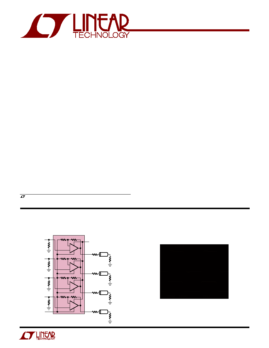
+
R
OUT
3.3V
OA
450
450
75
+
G
OUT
OA
450
450
75
+
B
OUT
OA
450
450
75
+
SYNC
OUT
R
IN
G
IN
B
IN
SYNC
IN
GND
OA
450
450
75
75
75
75
75
75
75
75
75
LT6551
6551 TA01a
V
IN
V
OUT
0V
0V
V
S
= 3.3V
V
IN
= 0.5V TO 1.25V
f = 10MHz
6550/51 TA01b
3.3V Single Supply LT6551 RGB Plus SYNC Cable Driver
Output Step Response
LT6550/LT6551
2
65501f
PARAMETER
CONDITIONS
MIN
TYP
MAX
UNITS
DC Output Accuracy
No Load, V
OUT
Ideal = 1.5V
q
30
70
mV
Output Voltage Matching
Between Any Two Outputs
q
25
75
mV
Input Current
Any Input
q
15
65
µ
A
Input Impedance,
V
IN
/
I
IN
V
IN
= 0V to 1V
q
100
300
k
Input Noise Voltage Density
f = 100kHz (Note 10)
12
nV/
Hz
Input Noise Current Density
f = 100kHz (Note 10)
8
pA/
Hz
Voltage Gain (Note 5)
0.25V
V
IN
1.25V
No Load
q
1.9
2.1
V/V
R
L
= 150
q
1.9
2.1
V/V
R
L
= 75
, 0.25V
V
IN
0.75V
1.85
2.15
V/V
Output Voltage Swing Low
V
IN
= 0.1V
No Load
q
10
30
mV
I
SINK
= 5mA
q
60
150
mV
I
SINK
= 10mA
q
90
200
mV
Output Voltage Swing High
V
IN
= 1.75V
No Load
q
3.0
3.2
V
R
L
= 150
q
2.5
2.9
V
R
L
= 75
2.0
2.5
V
Total Supply Voltage
LT6550 (V
CC
TO V
EE
) ........................................ 12.6V
LT6551 (V
CC
TO GND) ...................................... 12.6V
Input Current (Note 9) ........................................
±
10mA
Output Short-Circuit Duration (Note 2) ............ Indefinite
Operating Temperature Range ................ 40
°
C to 85
°
C
ORDER PART
NUMBER
MS10 PART
MARKING
LTB9
LTC1
LT6550CMS
LT6550IMS
ABSOLUTE AXI U
RATI GS
W
W
W
U
PACKAGE/ORDER I FOR ATIO
U
U
W
(Note 1)
The
q
denotes the specifications which apply over the specified
temperature range, otherwise specifications are at T
A
= 25
°
C. V
CC
= 3.3V, V
GND
= 0V; V
IN
= 0.75V LT6550 (Pins 1,2,3);
LT6551 (Pins 1,2,3,4). V
EE
= 0V LT6550 (Pin 5), unless otherwise noted.
Consult LTC Marketing for parts specified with wider operating temperature ranges.
ORDER PART
NUMBER
MS10 PART
MARKING
T
JMAX
= 150
°
C,
JA
= 110
°
C/W
(Note 4)
LTC2
LTC3
Specified Temperature Range (Note 3)
LT6550C/LT6551C ..............................40
°
C to 85
°
C
LT6550I/LT6551I ................................ 40
°
C to 85
°
C
Maximum Junction Temperature .......................... 150
°
C
Storage Temperature Range ................. 65
°
C to 150
°
C
Lead Temperature (Soldering, 10 sec).................. 300
°
C
LT6551CMS
LT6551IMS
T
JMAX
= 150
°
C,
JA
= 110
°
C/W
(Note 4)
1
2
3
4
5
IN1
IN2
IN3
GND
V
EE
10
9
8
7
6
V
CC
OUT1
OUT2
OUT3
N/C
TOP VIEW
MS10 PACKAGE
10-LEAD PLASTIC MSOP
X2
X2
X2
1
2
3
4
5
IN1
IN2
IN3
IN4
GND
10
9
8
7
6
V
CC
OUT1
OUT2
OUT3
OUT4
TOP VIEW
MS10 PACKAGE
10-LEAD PLASTIC MSOP
X2
X2
X2
X2
3.3V ELECTRICAL CHARACTERISTICS
LT6550/LT6551
3
65501f
The
q
denotes the specifications which apply over the specified
temperature range, otherwise specifications are at T
A
= 25
°
C. V
CC
= 3.3V, V
GND
= 0V; V
IN
= 0.75V LT6550 (Pins 1,2,3);
LT6551 (Pins 1,2,3,4). V
EE
= 0V LT6550 (Pin 5), unless otherwise noted.
3.3V ELECTRICAL CHARACTERISTICS
The
q
denotes the specifications which apply over the specified
temperature range, otherwise specifications are at T
A
= 25
°
C. V
CC
= 5V, V
GND
= 0V; V
IN
= 1.25V LT6550 (Pins 1,2,3);
LT6551 (Pins 1,2,3,4). V
EE
= 0V LT6550 (Pin 5), unless otherwise noted.
5V ELECTRICAL CHARACTERISTICS
PARAMETER
CONDITIONS
MIN
TYP
MAX
UNITS
PSRR
V
CC
= 3V to 10V, V
IN
= 0.5V
q
40
48
dB
Minimum Supply Voltage (Note 6)
q
3
V
Output Short-Circuit Current
V
IN
= 1V, V
OUT
= 0V
35
50
mA
q
25
mA
Supply Current per Amplifier (Note 7)
8.5
10
mA
q
11
mA
Slew Rate (Note 8)
R
L
= 150
, V
OUT
= 0.5V to 2.5V
140
250
V/
µ
s
Measured from 1V to 2V
q
115
V/
µ
s
Small Signal 3dB Bandwidth
R
L
= 150
90
MHz
Gain Flatness
Less than 0.25dB
30
MHz
Gain Matching
Any One Channel to Any Other Channel
0.15
dB
Settling Time to 3%
R
L
= 150
, V
OUT
= 1V to 2.5V
20
ns
Settling Time to 1%
R
L
= 150
, V
OUT
= 1V to 2.5V
30
ns
% Overshoot
V
OUT
= 1V to 2.5V, R
L
= 150
5
%
Differential Gain
R
L
= 150
, Black Level = 0.6V at Device Output
0.09
%
Differential Phase
R
L
= 150
, Black Level = 0.6V at Device Output
0.09
Deg
Channel Separation
Measured at 10MHz
60
dB
PARAMETER
CONDITIONS
MIN
TYP
MAX
UNITS
Output Accuracy
No Load, V
OUT
Ideal = 2.5V
q
30
70
mV
Output Voltage Matching
Between Any Two Outputs
q
40
90
mV
Input Current
q
15
65
µ
A
Input Impedance,
V
IN
/
I
IN
V
IN
= 0V to 2V
q
100
300
k
Input Noise Voltage Density
f = 100kHz (Note 10)
12
nV/
Hz
Input Noise Current Density
f = 100kHz (Note 10)
8
pA/
Hz
Voltage Gain (Note 5)
0.25V
V
IN
1.75V
No Load
q
1.9
2.1
V/V
R
L
= 150
q
1.9
2.1
V/V
R
L
= 75
, 0.25V
V
IN
1.25V, 0
°
C
T
A
70
°
C (Only)
q
1.85
2.15
V/V
Output Voltage Swing Low
V
IN
= 0.1V
No Load
q
10
30
mV
I
SINK
= 5mA
q
60
150
mV
I
SINK
= 10mA
q
90
200
mV
Output Voltage Swing High
V
IN
= 2.6V
No Load
q
4.6
4.8
V
R
L
= 150
q
3.5
4.1
V
R
L
= 75
, 0
°
C
T
A
70
°
C (Only)
q
2.5
3.2
V
PSRR
V
CC
= 3V to 10V, V
IN
= 0.5V
q
40
48
dB
Minimum Supply Voltage (Note 6)
q
3
V
LT6550/LT6551
4
65501f
(LT6550 Only) The
q
denotes the specifications which apply over
the specified temperature range, otherwise specifications are at T
A
= 25
°
C. V
S
=
±
5V, V
IN
= 0V (Pins 1,2,3) V
GND
= 0V (Pin 4) unless
otherwise noted.
5V ELECTRICAL CHARACTERISTICS
The
q
denotes the specifications which apply over the specified
temperature range, otherwise specifications are at T
A
= 25
°
C. V
CC
= 5V, V
GND
= 0V; V
IN
= 1.25V LT6550 (Pins 1,2,3);
LT6551 (Pins 1,2,3,4). V
EE
= 0V LT6550 (Pin 5), unless otherwise noted.
±
5V ELECTRICAL CHARACTERISTICS
PARAMETER
CONDITIONS
MIN
TYP
MAX
UNITS
Output Short-Circuit Current
V
IN
= 1V, V
OUT
= 0V
45
60
mA
0
°
C
T
A
70
°
C
q
40
mA
40
°
C
T
A
85
°
C
q
30
mA
Supply Current per Amplifier (Note 7)
9.5
11.5
mA
q
12.5
mA
Slew Rate
R
L
= 150
, V
OUT
= 0.5V to 3.5V,
220
340
V/
µ
s
Measured from 1V to 3V
q
180
V/
µ
s
Small Signal 3dB Bandwidth
R
L
= 150
110
MHz
Gain Flatness
Less than 0.25dB
30
MHz
Gain Matching
Any One Channel to Any Other Channel
0.15
dB
Settling Time to 3%
R
L
= 150
, V
OUT
= 1V to 2.5V
20
ns
Settling Time to 1%
R
L
= 150
, V
OUT
= 1V to 2.5V
35
ns
% Overshoot
V
OUT
= 1V to 2.5V, R
L
= 150
5
%
Differential Gain
R
L
= 150
, Black Level = 1V at Device Output
0.05
%
Differential Phase
R
L
= 150
, Black Level = 1V at Device Output
0.05
Deg
Channel Separation
Measured at 10MHz
60
dB
PARAMETER
CONDITIONS
MIN
TYP
MAX
UNITS
Output Offset
q
30
70
mV
Output Voltage Matching
Between Any Two Outputs
q
20
60
mV
Input Current
q
20
70
µ
A
Input Impedance,
V
IN
/
I
IN
V
IN
= 1V to 1V
q
200
500
k
Input Noise Voltage Density
f = 100kHz (Note 10)
12
nV/
Hz
Input Noise Current Density
f = 100kHz (Note 10)
8
pA/
Hz
Voltage Gain
1.75V
V
IN
1.75V
No Load
q
1.9
2.1
V/V
R
L
= 150
q
1.9
2.1
V/V
R
L
= 75
, 1V
V
IN
1V
q
1.9
2.1
V/V
Output Voltage Swing
V
IN
=
±
2.6V
No Load
q
±
4.6
±
4.8
V
R
L
= 150
q
±
3.5
±
4.2
V
R
L
= 75
, 0
°
C
T
A
70
°
C (Only)
q
±
2.6
±
3.2
V
PSRR
V
S
=
±
2.5V to
±
5V,
q
38
48
dB
Output Short-Circuit Current
V
O
= 0V
45
60
mA
0
°
C
T
A
70
°
C
q
40
mA
40
°
C
T
A
85
°
C
q
30
mA
Supply Current per Amplifier
8.5
10.5
mA
q
12
mA
Slew Rate
R
L
= 150
, V
OUT
= 3V to 3V,
400
600
V/
µ
s
Measured from 2V to 2V
q
300
V/
µ
s
Small Signal 3dB Bandwidth
R
L
= 150
90
MHz
LT6550/LT6551
5
65501f
Note 1: Absolute Maximum Ratings are those values beyond which the life
of a device may be impaired.
Note 2: A heat sink may be required to keep the junction temperature
below absolute maximum. This depends on the power supply voltage and
how many amplifiers are shorted.
Note 3: The LT6550C/LT6551C are guaranteed to meet specified
performance from 0
°
C to 70
°
C and are designed, characterized and
expected to meet specified performance from 40
°
C to 85
°
C but are not
tested or QA sampled at these temperatures. The LT6550I/LT6551I are
guaranteed to meet specified performance from 40
°
C to 85
°
C.
Note 4: Thermal resistance varies depending upon the amount of PC board
metal attached to Pin 5 of the device.
JA
is specified for a 2500mm
2
test
board covered with 2oz copper on both sides.
Note 5: Gain is measured by changing the input voltage, and dividing the
change in output voltage by the change in input voltage.
Note 6: Minimum supply voltage is guaranteed by the PSRR test.
Note 7: The supply current specification includes additional output current
through the internal feedback and gain resistor.
Note 8: Guaranteed by correlation to slew rate at 5V and
±
5V.
Note 9: The inputs are protected from ESD with diodes to the supplies.
Note 10: Noise is input referred, including internal gain resistors.
(LT6550 Only) The
q
denotes the specifications which apply over
the specified temperature range, otherwise specifications are at T
A
= 25
°
C. V
S
=
±
5V, V
IN
= 0V (Pins 1,2,3) V
GND
= 0V (Pin 4) unless
otherwise noted.
±
5V ELECTRICAL CHARACTERISTICS
PARAMETER
CONDITIONS
MIN
TYP
MAX
UNITS
Gain Flatness
Less than 0.25dB
30
MHz
Gain Matching
Any One Channel to Any Other Channel
0.15
dB
Settling Time to 3%
R
L
= 150
, V
OUT
= 1V to 2.5V
20
ns
Settling Time to 1%
R
L
= 150
, V
OUT
= 1V to 2.5V
30
ns
% Overshoot
V
OUT
= 1V to 2.5V, R
L
= 150
5
%
Differential Gain
R
L
= 150
, Black Level = 0V at Device Output
0.15
%
Differential Phase
R
L
= 150
, Black Level = 0V at Device Output
0.09
Deg
Channel Separation
Measured at 10MHz
60
dB
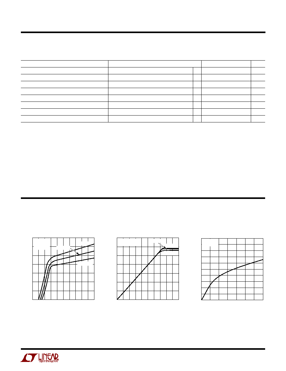
Supply Current Per Amplifier vs
Supply Voltage
Output Voltage vs Input Voltage
Input Bias Current vs
Temperature
V
CC
(V)
0
SUPPLY CURRENT (mA)
14
12
10
8
6
4
2
0
6550/51 G01
2
10
9
8
7
6
5
1
3
4
V
IN
(V)
0
V
OUT
(V)
3.5
3.0
2.5
2.0
1.5
1.0
0.5
0
6550/51 G02
0.4
2.0
1.8
1.6
1.4
1.2
1.0
0.2
0.6 0.8
TEMPERATURE (
°
C)
50
INPUT BIAS (
µ
A)
10
11
12
13
14
15
16
17
18
19
20
0
50
75
6550/51 G03
25
25
100
125
T
A
= 55
°
C
T
A
= 25
°
C
V
S
= 3.3V, 0V
R
L
= 150
V
IN
= 0.75V
R
L
=
GND = 0V
V
S
= 5V, 0V
V
OUT
= 2.5V
T
A
= 125
°
C
T
A
= 55
°
C
T
A
= 25
°
C
T
A
= 125
°
C
5V/3.3V TYPICAL PERFOR A CE CHARACTERISTICS
U
W
V
EE
(Pin 5) = 0V (LT6550), GND (Pin 5) = 0V (LT6551)