 | ÐлекÑÑоннÑй компоненÑ: LT6650 | СкаÑаÑÑ:  PDF PDF  ZIP ZIP |
Äîêóìåíòàöèÿ è îïèñàíèÿ www.docs.chipfind.ru
LT6650
1
6650f
APPLICATIO S
U
FEATURES
TYPICAL APPLICATIO
U
DESCRIPTIO
U
The LT
®
6650 is a micropower, low voltage 400mV refer-
ence. Operating with supplies from 1.4V up to 18V, the
device draws only 5.6
µ
A typical, making it ideal for low
voltage systems as well as handheld instruments and
industrial control systems. With only two resistors the
internal buffer amplifier can scale the 400mV reference to
any desired value up to the supply voltage.
The reference is postpackage-trimmed to increase the
output accuracy. The output can sink and source 200
µ
A
over temperature. Quiescent power dissipation is 28
µ
W.
Stability is ensured with any output capacitor of 1
µ
F or
higher.
The LT6650 is the lowest voltage series reference available
in the 5-lead SOT-23 package.
s
Battery-Operated Systems
s
Handheld Instruments
s
Industrial Control Systems
s
Data Acquisition Systems
s
Negative Voltage References
, LTC and LT are registered trademarks of Linear Technology Corporation.
s
Low Quiescent Current 5.6
µ
A (typical)
s
Wide Supply Range: 1.4V to 18V
s
400mV Reference
±
1% Maximum Accuracy Over
Temperature at 5V
s
Rail-to-Rail Buffer Amplifier
s
0.5% 400mV Maximum Initial Accuracy at 5V
s
Shunt Configurable
s
Sinks and Sources Current
s
Wide Operational Range 40
°
C to 125
°
C
s
Externally Adjustable Output Voltage
s
Low Profile 1mm 5-lead SOT-23
(ThinSOTTM) Package
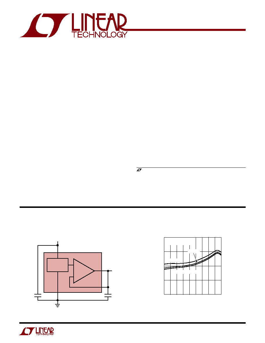
Micropower, 400mV
Reference with Rail-to-Rail
Buffer Amplifier in SOT-23
ThinSOT is a trademark of Linear Technology Corporation.
OUT
V
OUT
0.4V
V
IN
= 1.4V TO 18V
I
Q
6
µ
A
5
1
FB
IN
4
GND
1
µ
F
2
LT6650
+
1
µ
F
V
R
= 400mV
REFERENCE
6650 TA01a
TEMPERATURE (
°
C)
REFERENCE VOLTAGE (mV)
402
401
400
398
399
30
10
50
90
6650 TA01b
130
50
10
30
70
110
TYPICAL LT6650 PART
V
IN
= 5V
SINK 200
µ
A
SOURCE 200
µ
A
NO LOAD
LT6650 Temperature Drift
Battery-Powered 0.4V Reference
LT6650
2
6650f
Total Supply Voltage (V
IN
to GND) ........................... 20V
FB Voltage (Note 2) ....................... 20V to (GND 0.3V)
Output Voltage (OUT) .................... 20V to (GND 0.3V)
Output Short Circuit Duration .......................... Indefinite
FB Input Current ................................................... 10mA
Operating Temperature Range ............... 40
°
C to 125
°
C
Specified Temperature Range
LT6650CS5 ............................................. 0
°
C to 70
°
C
LT6650IS5 ........................................... 40
°
C to 85
°
C
LT6650HS5 (Note 3) ......................... 40
°
C to 125
°
C
Maximum Junction Temperature .......................... 150
°
C
Storage Temperature Range
(Note 4) ............................................. 65
°
C to 150
°
C
Lead Temperature (Soldering, 10 sec).................. 300
°
C
ORDER PART
NUMBER
S5 PART
MARKING
T
JMAX
= 150
°
C,
JA
= 230
°
C/W
The temperature grades are identified by a label on the shipping container.
Consult LTC Marketing for parts specified with wider operating temperature ranges.
LBDV
LT6650CS5
LT6650IS5
LT6650HS5
ABSOLUTE AXI U
RATI GS
W
W
W
U
PACKAGE/ORDER I FOR ATIO
U
U
W
(Note 1)
ELECTRICAL CHARACTERISTICS
The
q
denotes the specifications which apply over the full operating
temperature range, otherwise specifications are at T
A
= 25
°
C. V
IN
= 5V, C
IN
= 1
µ
F, FB = OUT, no DC load, C
L
= 1
µ
F, unless
otherwise noted.
SYMBOL
PARAMETER
CONDITIONS
MIN
TYP
MAX
UNITS
V
OUT
Output Voltage (Notes 4, 5)
LT6650
398
400
402
mV
0.5
0.5
%
LT6650CS5
q
397
400
403
mV
q
0.75
0.75
%
LT6650IS5
q
396
400
404
mV
q
1
1
%
LT6650HS5
q
394
400
406
mV
q
1.5
1.5
%
V
IN
Operating Input Voltage
1.4
18
V
V
OUT
/
V
IN
Line Regulation
1.4V
V
IN
18V
1
6
mV
150
900
ppm/V
LT6650CS5, LT6650IS5
q
7.5
mV
q
1130
ppm/V
LT6650HS5
q
8.5
mV
q
1280
ppm/V
V
OUT
/
I
OUT
Load Regulation (Note 6)
Sourcing from 0
µ
A to 200
µ
A
0.04
0.2
mV
500
2500
ppm/mA
q
0.4
mV
q
5000
ppm/mA
Sinking from 0
µ
A to 200
µ
A
0.24
1
mV
3000
12500
ppm/mA
q
2
mV
q
20000
ppm/mA
T
C
Output Voltage Temperature
q
30
ppm/
°
C
Coefficient (Note 10)
TOP VIEW
S5 PACKAGE
5-LEAD PLASTIC TSOT-23
1
2
3
FB
GND
DNC*
5
4
OUT
IN
*Do Not Connect
LT6650
3
6650f
V
DO
Dropout Voltage (Note 7)
Referred to V
IN
= 1.8V, V
OUT
= 1.4V
(R
F
= 100k, R
G
= 39.2k)
V
OUT
= 0.1%, I
OUT
= 0
µ
A
75
100
mV
q
150
mV
V
OUT
= 0.1%, I
OUT
= 200
µ
A Sourcing
165
250
mV
q
350
mV
V
OUT
= 0.1%, I
OUT
= 200
µ
A Sinking (Note 11)
300
150
mV
q
0
mV
I
SC
Short-Circuit Output Current
V
OUT
Shorted to GND
5
mA
V
OUT
Shorted to V
IN
9
mA
I
IN
Supply Current
5.6
11
µ
A
q
14
µ
A
V
IN
= 18V
5.9
12
µ
A
q
15
µ
A
I
FB
FB Pin Input Current
V
FB
= V
OUT
= 400mV
1.2
10
nA
LT6650CS5, LT6650IS5
q
15
nA
LT6650HS5
q
30
nA
T
ON
Turn-On Time
C
LOAD
= 1
µ
F
0.5
ms
e
n
Output Noise (Note 8)
0.1Hz
10Hz
20
µ
V
P-P
10Hz
1KHz, I
OUT
= 200
µ
A Sourcing
23
µ
V
RMS
V
HYS
Hysteresis (Note 9)
T = 0
°
C to 70
°
C
q
0.1
mV
q
250
ppm
T = 40
°
C to 85
°
C
q
0.24
mV
q
600
ppm
Note 1: Absolute Maximum Ratings are those values beyond which the life
of a device may be impaired.
Note 2: The FB pin is protected by an ESD diode to the ground. If the FB
input voltage exceeds 0.3V below ground, the FB input current should be
limited to less than 10mA. If the FB input voltage is greater than 5V, the FB
input current is expected to meet specified performance from Typical
Performance Characteristics but is not tested or QA sampled at this
voltage.
Note 3: If the part is operating at temperatures above 85
°
C, it is
recommended to enhance the stability margin by using an output
capacitor greater than 10
µ
F or a series RC combination having a 100
µ
s
equivalent time constant. See Application section for details.
Note 4: If the part is stored outside of the specified temperature range, the
output voltage may shift due to hysteresis.
Note 5: ESD (Electrostatic Discharge) sensitive devices. Extensive use of
ESD protection devices are used internal to the LT6650; however, high
electrostatic discharge can damage or degrade the device. Use proper ESD
handling precautions.
ELECTRICAL CHARACTERISTICS
The
q
denotes the specifications which apply over the full operating
temperature range, otherwise specifications are at T
A
= 25
°
C. V
IN
= 5V, C
IN
= 1
µ
F, FB = OUT, no DC load, C
L
= 1
µ
F, unless
otherwise noted.
SYMBOL
PARAMETER
CONDITIONS
MIN
TYP
MAX
UNITS
Note 6: Load regulation is measured on a pulse basis from no load to the
specified load current. Output changes due to die temperature change
must be taken into account separately.
Note 7: Dropout Voltage is (V
IN
V
OUT
) when V
OUT
falls to 0.1% below its
nominal value at V
IN
= 1.8V.
Note 8: Peak-to-Peak noise is measured with a single pole highpass filter
at 0.1Hz and a 2-pole lowpass filter at 10Hz. The unit is enclosed in a still
air environment to eliminate thermocouple effects on the leads. The test
time is 10 seconds.
Note 9: Hysteresis in the output voltage is created by package stress that
differs depending on whether the IC was previously at a higher or lower
temperature. Output voltage is always measured at 25
°
C, but the IC is
cycled to 85
°
C or 40
°
C before a successive measurement. Hysteresis is
roughly proportional to the square of the temperature change.
Note 10: Temperature coefficient is measured by dividing the change in
output voltage by the specified temperature range.
Note 11: This feature guarantees the shunt mode operation of the device.
LT6650
4
6650f
INPUT VOLTAGE (V)
0
SUPPLY CURRENT (
µ
A)
6
8
10
16
6650 G03
4
2
0
4
8
12
20
14
2
6
10
18
125
°
C
55
°
C
25
°
C
TEMPERATURE (
°
C)
60
OUTPUT VOLTAGE (mV)
404
403
402
400
401
399
398
397
396
100
6650 G01
20
40
0
40
80
120
20
60
TYPICAL PART
V
IN
= 1.4V
V
IN
= 5V
V
IN
= 18V
TEMPERATURE (
°
C)
60
OUTPUT VOLTAGE (mV)
403
402
400
401
399
398
100
6650 G02
20
40
0
40
80
120
20
60
THREE PARTS
V
IN
= 5V
INPUT VOLTAGE (V)
0
SUPPLY CURRENT (
µ
A)
6
8
10
1.6
6650 G04
4
2
0
0.4
0.8
1.2
2.0
1.4
0.2
0.6
1.0
1.8
125
°
C
55
°
C
25
°
C
INPUT VOLTAGE (V)
2
398
OUTPUT VOLTAGE (mV)
399
400
401
402
6
10
14
18
6550 G05
403
404
4
8
12
16
T
A
= 125
°
C
T
A
= 55
°
C
T
A
= 25
°
C
INPUT VOLTAGE (V)
0.8
398
OUTPUT VOLTAGE (mV)
399
400
401
402
1.2
1.6
2.0
1.8
6650 G06
403
404
1.0
1.4
T
A
= 125
°
C
T
A
= 55
°
C
T
A
= 25
°
C
OUTPUT CURRENT (
µ
A)
10
OUTPUT VOLTAGE CHANGE (
µ
V)
0
10
20
30
40
50
60
70
80
90
100
100
1000
6650 G07
TYPICAL PART
V
IN
= 5V
125
°
C
55
°
C
25
°
C
OUTPUT CURRENT (
µ
A)
10
OUTPUT VOLTAGE CHANGE (
µ
V)
1000
900
800
700
600
500
400
300
200
100
0
100
1000
6650 G08
TYPICAL PART
V
IN
= 5V
125
°
C
55
°
C
25
°
C
OUTPUT CURRENT (
µ
A)
10
INPUT-OUTPUT VOLTAGE (mV)
500
400
300
200
100
0
100
1000
6650 G09
V
OUT
= 1.425V - TYP (RF = 100k, RG = 39.2k)
0.1% V
OUT
125
°
C
55
°
C
25
°
C
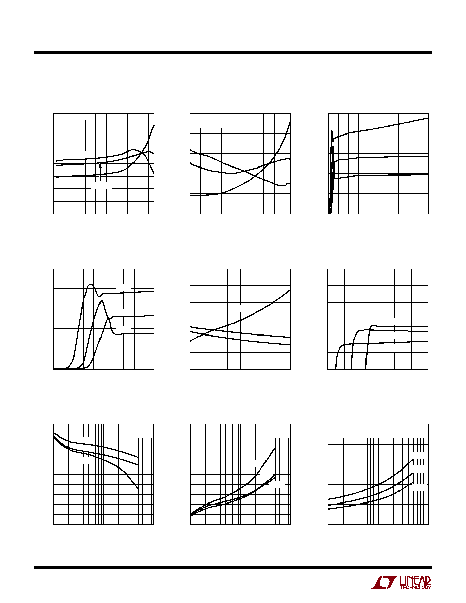
Output Voltage Temperature
Drift
Output Voltage Temperature
Drift
Supply Current vs Input Voltage
Line Regulation
Line Regulation
Load Regulation (Sourcing)
Load Regulation (Sinking)
Minimum Input-Output Voltage
Differential (Sourcing)
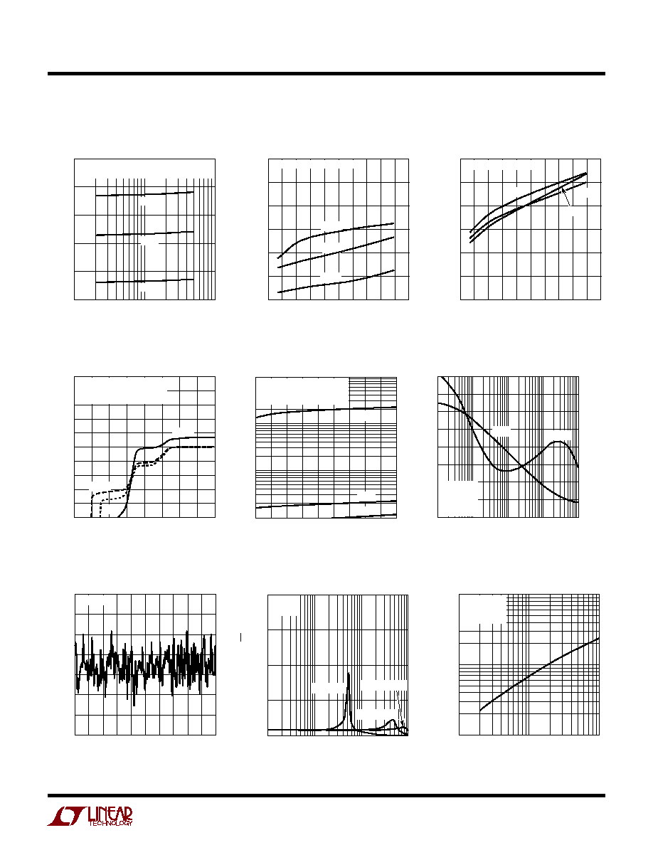
TYPICAL PERFOR A CE CHARACTERISTICS
U
W
(See Applications, Figure 1)
Supply Current vs Input Voltage
LT6650
5
6650f
Minimum Input-Output Voltage
Differential (Sinking)
Output Short Circuit Current vs
Input Voltage
Output Short Circuit Current vs
Input Voltage
FB Pin Current vs FB Pin Voltage
FB Pin Current vs FB Pin Voltage
Gain and Phase vs Frequency
Output Noise 0.1Hz to 10Hz
Output Voltage Noise Spectrum
Integrated Noise 10Hz to 1kHz
OUTPUT CURRENT(
µ
A)
10
100
1000
INPUT-OUTPUT VOLTAGE (mV)
0
400
300
200
100
500
6650 G10
V
OUT
= 1.425V - TYP (RF = 100k, RG = 39.2k)
0.1% V
OUT
125
°
C
55
°
C
25
°
C
INPUT VOLTAGE (V)
0
OUTPUT CURRENT (mA)
6
8
14
12
10
16
6650 G11
4
2
4
8
12
20
14
2
6
10
18
OUTPUT SHORTED TO GND
125
°
C
55
°
C
25
°
C
INPUT VOLTAGE (V)
0
OUTPUT CURRENT (mA)
6
8
14
12
10
16
6650 G12
4
2
4
8
12
20
14
2
6
10
18
OUTPUT SHORTED TO V
IN
125
°
C
25
°
C
55
°
C
FB PIN VOLTAGE (V)
0.6
10
FB PIN CURRENT (nA)
0
2
4
6
0.2
0.2
0.6
1.0
6650 G13
8
2
4
6
8
10
0.4
0
0.4
0.8
125
°
C
V
FB
V
OUT
CURRENT IS POSITIVE WHEN
IT ENTERS THE DEVICE
55
°
C
25
°
C
FB PIN VOLTAGE (V)
1
3
7
9
5
15
13
11
17
19
FB PIN CURRENT (nA)
10
1
0.1
0.01
6650 G14
125
°
C
V
FB
V
OUT
CURRENT IS POSITIVE WHEN
IT ENTERS THE DEVICE
55
°
C
25
°
C
FREQUENCY (kHz)
GAIN (dB)
120
100
80
60
40
20
0
0
20
40
PHASE (DEG)
120
100
80
60
40
20
20
40
0.01
1
10
100
6650 G15
0.1
T
A
= 25
°
C
UNITY GAIN
R
L
= 2k
C
L
= 1
µ
F
GAIN
PHASE
TIME (s)
0
OUTPUT NOISE (5
µ
V/DIV)
8
6650 G16
2
4
6
10
7
1
3
5
9
V
IN
= 5V
FREQUENCY (Hz)
10
NOISE LEVEL (
µ
V/
Hz)
20
100
1k
10k
6650 G17
V
IN
= 5V
C
L
= 1
µ
F
I
OUT
= 40
µ
A
I
OUT
= 0
µ
A
0
5
10
15
I
OUT
= 200
µ
A
FREQUENCY (Hz)
10
1
INTEGRATED NOISE (
µ
V
RMS
)
10
100
100
1k
6650 G18
V
IN
= 5V
C
L
= 1
µ
F
I
OUT
= 200
µ
A
TYPICAL PERFOR A CE CHARACTERISTICS
U
W
(See Applications, Figure 1)