 | ÐлекÑÑоннÑй компоненÑ: LTC1040 | СкаÑаÑÑ:  PDF PDF  ZIP ZIP |
LTC1040fa.pm65
1
LTC1040
1040fa
s
Micropower
1.5
µ
W (1 Sample/Second)
s
Power Supply Flexibility
Single Supply 2.8V to 16V
Split Supply
±
2.8V to
±
8V
s
Guaranteed Max Offset 0.75mV
s
Guaranteed Max Tracking Error Between Input
Pairs
±
0.1%
s
Input Common Mode Range to Both Supply Rails
s
TTL/CMOS Compatible with
±
5V or Single 5V
Supply
s
Input Errors are Stable with Time and Temperature
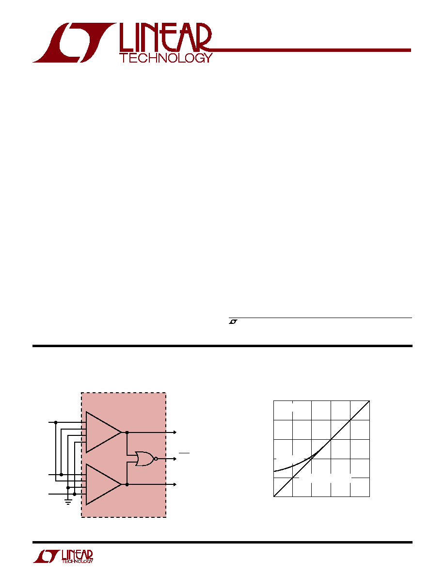
The LTC
®
1040 is a monolithic CMOS dual comparator
manufactured using Linear Technology's enhanced
LTCMOS
TM
silicon gate process. Extremely low operating
power levels are achieved by internally switching the
comparator ON for short periods of time. The CMOS
output logic holds the output information continuously
while not consuming any power.
In addition to switching power ON, a switched output is
provided to drive external loads during the comparator's
active time. This allows not only low comparator power,
but low total system power.
Sampling is controlled by an external strobe input or an
internal oscillator. The oscillator frequency is set by an
external RC network.
Each comparator has a unique input structure, giving two
differential inputs. The output of the comparator will be
high if the algebraic sum of the inputs is positive and low
if the algebraic sum of the inputs is negative.
Window Comparator with Symmetric Window Limits
Dual Micropower
Comparator
Typical LTC1040 Supply Current
vs Sampling Frequency
FEATURES
APPLICATIO S
U
DESCRIPTIO
U
s
Battery-Powered Systems
s
Remote Sensing
s
Window Comparator
s
BANG-BANG Controllers
, LTC and LT are registered trademarks of Linear Technology Corporation.
V
C
A
OUT
= "1" WHEN
V
IN
> V
C
+
B
OUT
= "1" WHEN
V
IN
< V
C
A + B = "1" WHEN
V
C
V
IN
V
C
+
V
IN
LTC1040 · TA01
+
+
+
+
COMP A
COMP B
LTC1040
SAMPLING FREQUENCY, f
S
(Hz)
0.1
SUPPLY CURRENT, I
S
(
µ
A)
10
100
1000
1,000
LTC1040 · TA02
1
0.10
0.01
1
10
100
10,000
V
S
=
±
5V
R
EXT
= 10M
EXTERNALLY STROBED
TYPICAL APPLICATIO
U
LTCMOSTM is a trademark of Linear Technology Corporation.
2
LTC1040
1040fa
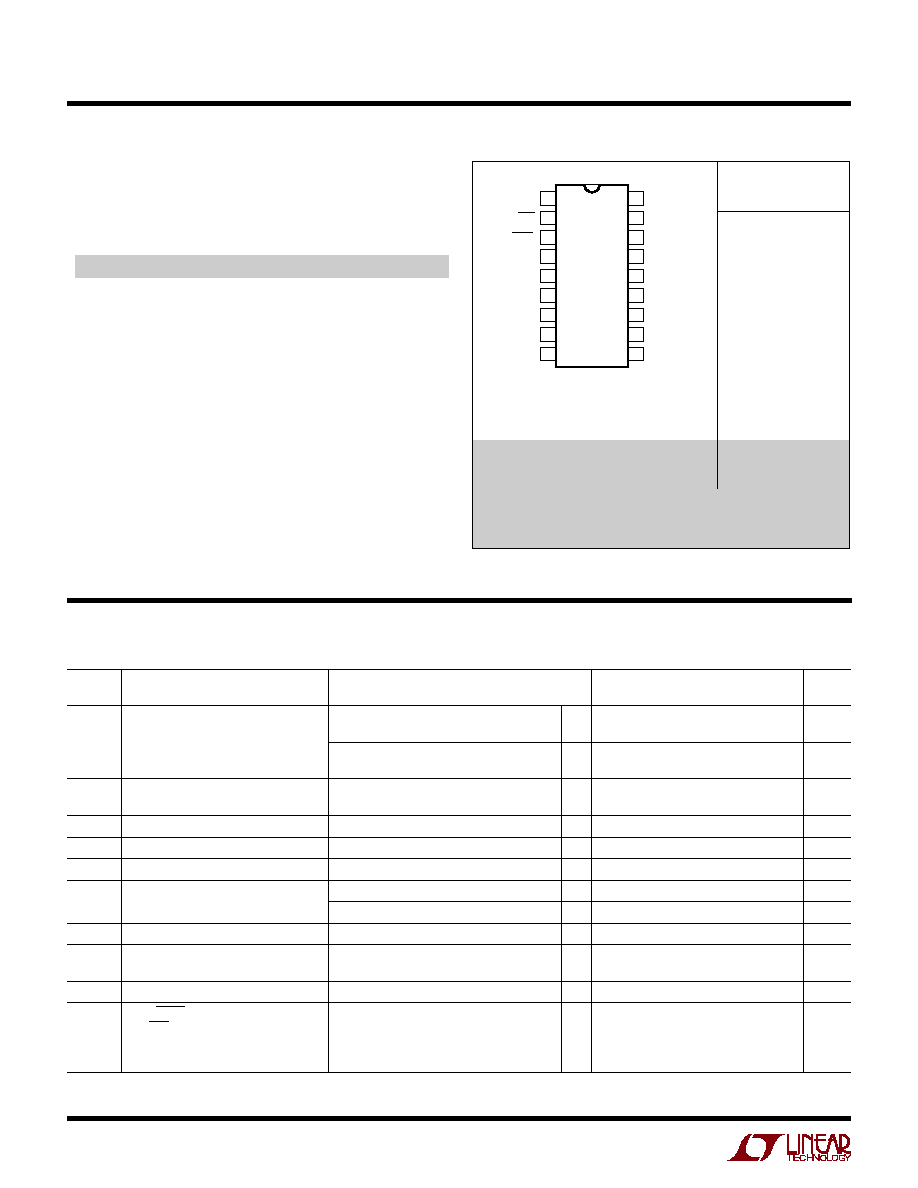
ORDER PART
NUMBER
LTC1040CN
LTC1040CSW
LTC1040MJ
LTC1040CJ
N PACKAGE
18-LEAD PDIP
TOP VIEW
1
2
3
4
5
6
7
8
9
18
17
16
15
14
13
12
11
10
STROBE
ON/OFF
A + B
A
OUT
A1
+
A1
A2
+
A2
GND
V
+
V
P-P
OSC
B
OUT
B1
+
B1
B2
+
B2
V
J PACKAGE
18-LEAD CERDIP
T
JMAX
= 150
°
C,
JA
= 80
°
C/W
SW PACKAGE
18-LEAD PLASTIC SO WIDE
T
JMAX
= 110
°
C,
JA
= 120
°
C/W (N)
T
JMAX
= 125
°
C,
JA
= 85
°
C/W (SW)
Total Supply Voltage (V
+
to V
) ............................... 18V
lnput Voltage ........................ (V
+
+ 0.3V) to (V
0.3V)
Operating Temperature Range
LTC1040C ..................................... 40
°
C
T
A
85
°
C
LTC1040M (OBSOLETE) .................... 55
°
C to 125
°
C
Storage Temperature Range ................. 55
°
C to 150
°
C
Lead Temperature (Soldering, 10 sec).................. 300
°
C
Output Short-Circuit Duration ....................... Continuous
ABSOLUTE AXI U RATI GS
W
W
W
U
PACKAGE/ORDER I FOR ATIO
U
U
W
(Note 1)
ELECTRICAL CHARACTERISTICS
The
q
denotes the specifications which apply over the full operating
temperature range, otherwise specifications are at T
A
= 25
°
C. Test conditions: V
+
= 5V, V
= 5V, unless otherwise noted.
LTC1040M/LTC1040C
SYMBOL
PARAMETER
CONDITIONS
MIN
TYP
MAX
UNITS
V
OS
Offset Voltage (Note 2)
Split Supplies
±
2.8V to
±
6V
q
±
0.3
±
0.75
mV
Single Supply (V
= GND) 2.8V to 6V
Split Supplies
±
6V to
±
8V
q
±
1
±
4.5
mV
Single Supply (V
= GND) 6V to 15V
Tracking Error Between
Split Supplies
±
2.8V to
±
8V
q
0.05
0.1
%
Input Pairs (Notes 2 and 3)
Single Supplies (V
= GND) 2.8 to 16V
I
BIAS
Input Bias Current
OSC = GND
±
0.3
nA
R
IN
Average Input Resistance
f
S
= 1kHz (Note 4)
q
20
30
M
CMR
Common Mode Range
q
V
V
+
V
PSR
Power Supply Range
Split Supplies
q
±
2.8
±
8
V
Single Supplies (V
= GND)
q
2.8
16
V
I
S(ON)
Power Supply ON Current (Note 5)
V
+
= 5V, V
P-P
On
q
1.2
3
mA
I
S(OFF)
Power Supply OFF Current (Note 5)
V
+
= 5V, V
P-P
Off
LTC1040C
q
0.001
0.5
µ
A
LTC1040M
q
0.001
5
µ
A
t
D
Response Time (Note 6)
60
80
100
µ
s
A, B, A + B and
ON/OFF Outputs (Note 7)
V
OH
Logic "1" Output Voltage
V
+
= 4.75V, l
OUT
= 360
µ
A
q
2.4
4.4
V
V
OL
Logic "0" Output Voltage
V
+
= 4.75V, l
OUT
= 1.6mA
q
0.25
0.4
V
OBSOLETE PACKAGE
Consider the N18 Package as an Alternate Source
Consult LTC Marketing for parts specified with wider operating temperature ranges.
3
LTC1040
1040fa
Note 1: Absolute Maximum Ratings are those values beyond which the life
of a device may be impaired.
Note 2: Applies over input voltage range limit and includes gain
uncertainty.
Note 3: Tracking error = (V
IN1
V
IN2
)/ V
IN1
.
Note 4: R
IN
is guaranteed by design and is not tested.
R
IN
= 1/(f
S
· 33pF).
Note 5: Average supply current = t
D
· l
S(ON)
· f
S
+ (1 t
D
x f
S
) · l
S(OFF)
.
Note 6: Response time is set by an internal oscillator and is independent
of overdrive voltage.
Note 7: Inputs and outputs also capable of meeting EIA/JEDEC B series
CMOS specifications.
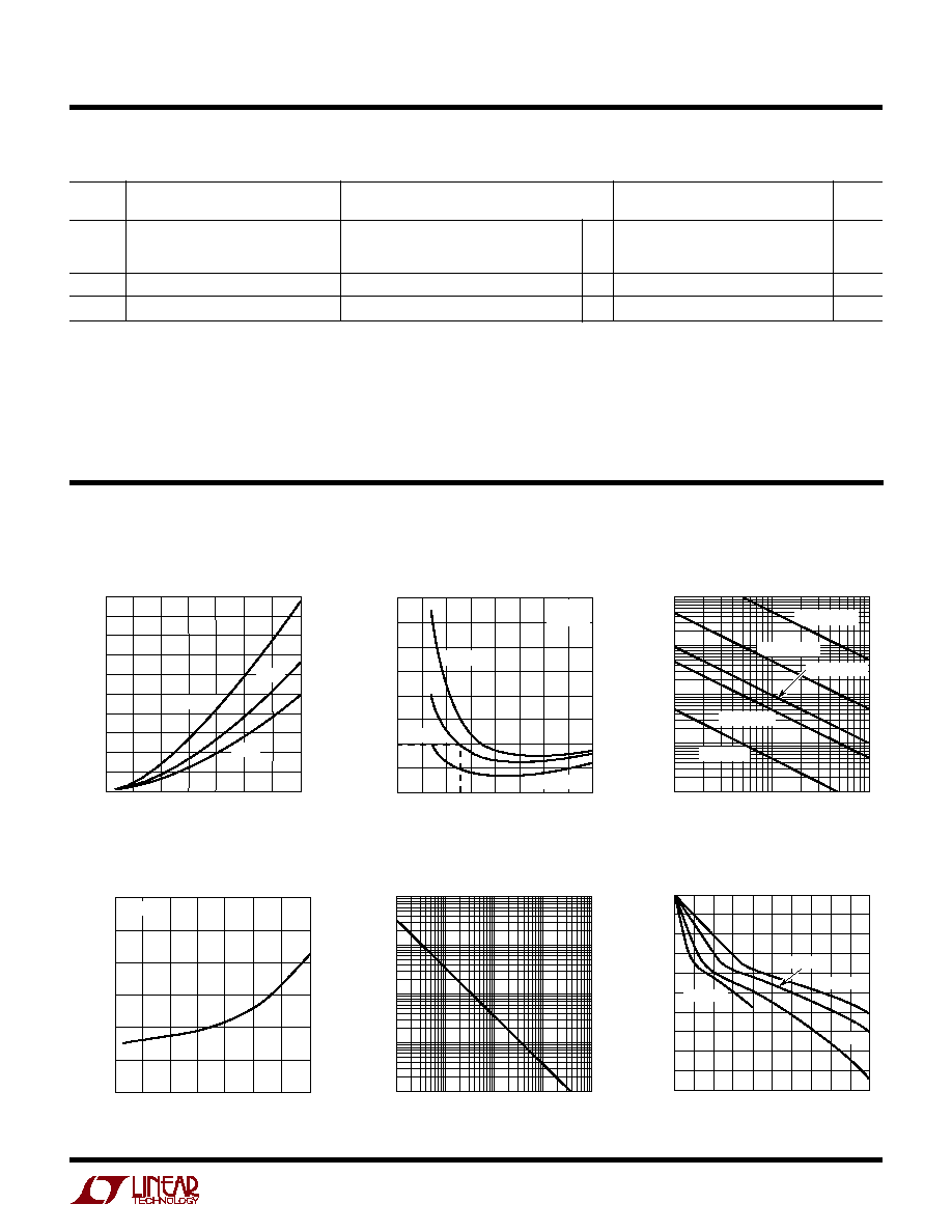
TYPICAL PERFOR A CE CHARACTERISTICS
U
W
Peak Supply Current
vs Supply Voltage
SUPPLY VOLTAGE, V
+
(V)
2
0
I
S(ON)
(mA)
2
6
8
10
20
14
6
10
12
LTC1040 · TPC01
4
16
18
12
4
8
14
16
25
°
C
125
°
C
55
°
C
LTC1040M/LTC1040C
SYMBOL
PARAMETER
CONDITIONS
MIN
TYP
MAX
UNITS
STROBE Input (Note 7)
V
IH
Logic "1" Input Voltage
V
+
= 5.25V
q
2.0
1.6
V
V
IL
Logic "0" Input Voltage
V
+
= 4.75V
1.0
0.8
V
R
EXT
External Timing Resistor
Resistor Tied Between V
+
and OSC Pin
q
100
10,000
k
f
S
Sampling Frequency
R
EXT
= 1M, C
EXT
= 0.1
µ
F
5
Hz
ELECTRICAL CHARACTERISTICS
The
q
denotes the specifications which apply over the full operating
temperature range otherwise specifications are at T
A
= 25
°
C. Test conditions: V
+
= 5V, V
= 5V, unless otherwise specified
Normalized Sampling Frequency
vs Supply Voltage and Temperature
SUPPLY VOLTAGE, V
+
(V)
0
(f
S
/f
S
AT 5V, 25
°
C)
NORMALIZED SAMPLING FREQUENCY
1.4
1.8
16
LTC1040 · TPC02
1.0
0.6
4
8
12
2
6
10
14
2.2
1.2
1.6
0.8
2.0
T
A
= 125
°
C
T
A
= 25
°
C
T
A
= 55
°
C
R = 1M
C = 0.1
µ
F
Input Resistance
vs Sampling Frequency
SAMPLING FREQUENCY, f
S
(Hz)
1
10
7
AVERAGE INPUT RESISTANCE, R
IN
(1/f
S
· 33pF) (
)
10
9
10
11
10
2
10
4
10
3
10
LTC1040 · TPC05
10
8
10
10
Sampling Rate vs R
EXT
, C
EXT
R
EXT
(
)
100k
0.1
1
10
10
2
SAMPLE RATE, f
S
(Hz)
10
3
1M
10M
LT1040 · TPC03
C
EXT
= 1000pF
C
EXT
= 0.01
µ
F
C
EXT
= 0.1
µ
F
C
EXT
= 1
µ
F
C
EXT
= 0.05
µ
F
Response Time
vs Supply Voltage
SUPPLY VOLTAGE, V
+
(V)
2
RESPONSE TIME, t
D
(
µ
s)
200
250
300
8
12
LTL1040 · TPC04
150
100
4
6
10
14
16
50
0
T
A
= 25
°
C
V
P-P
Output Voltage
vs Load Current
LOAD CURRENT, I
L
(mA)
0
TYPICAL OUTPUT VOLTAGE DROP, V
+
V
P-P
(V)
0.8
0.4
0
8
LTC1040 · TPC06
1.2
1.6
2.0
0.6
0.2
1.0
1.4
1.8
2
1
4
3
6
7
9
5
10
V
+
= 2.8V
V
+
= 16V
V
+
= 5V
V
+
= 10V
4
LTC1040
1040fa
TYPICAL PERFOR A CE CHARACTERISTICS
U
W
Response Time
vs Temperature
Self-Oscillating
Quick Hookup Guide
AMBIENT TEMPERATURE, T
A
(
°
C)
50
40
RESPONSE TIME, t
D
(
µ
s)
50
70
80
90
50
130
LTC1040 · TPC07
60
0
25
100
75
25
125
100
110
120
V
+
= 5V
18
17
16
10
R
EXT
EXTERNAL
STROBE
INPUT
C
EXT
LTC1040 · TPC08
1
9
LTC1040
1
9
18
17
16
10
LTC1040
V+
V+
External Strobe
TEST CIRCUIT
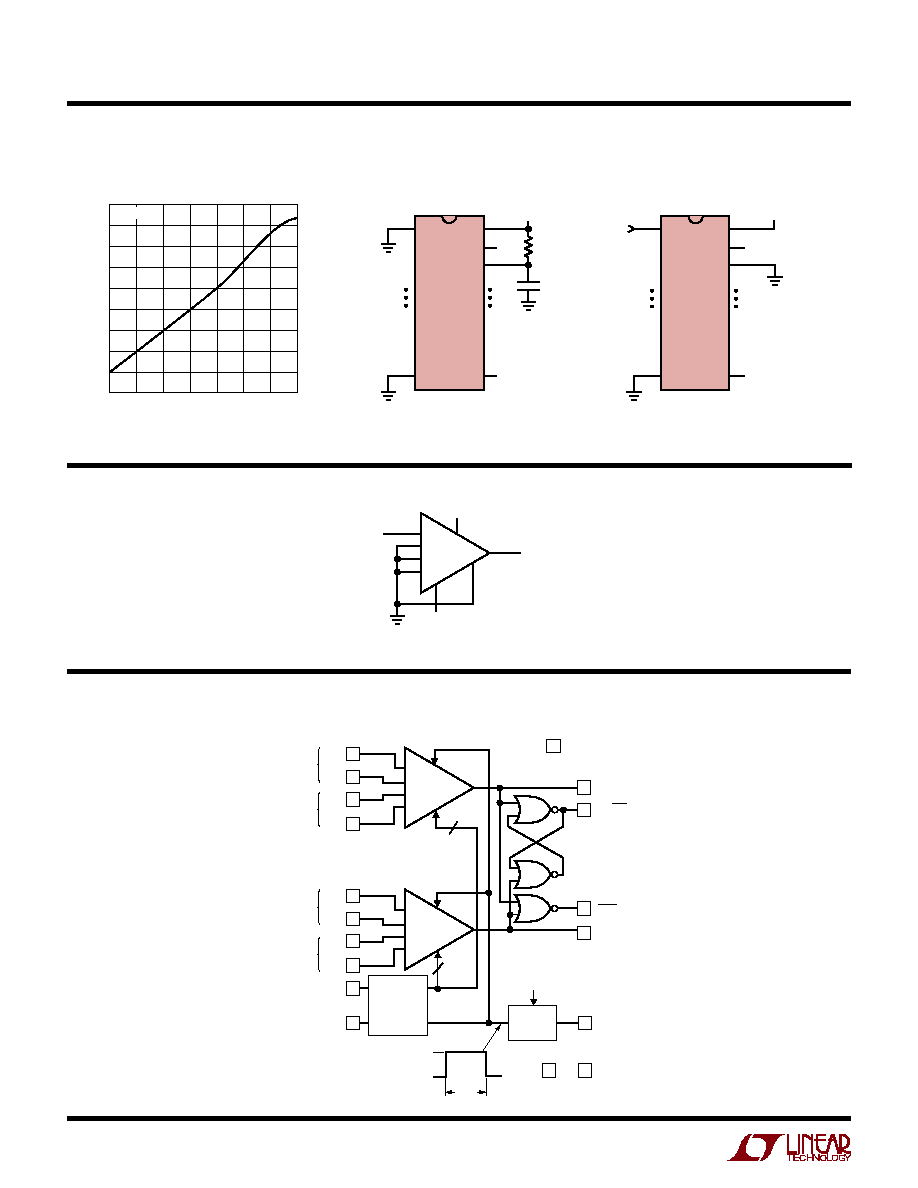
BLOCK DIAGRA
W
V
IN
LTC1040 · TA01
V
+
(18)
V
(10)
ALL INPUTS ON OPPOSITE COMPARATOR AT GROUND
GND (9)
OUTPUT
+
+
V
IN1
V
IN2
LTC1040 · BD01
A1
+
A1
A2
+
V
+
V
+
A2
+
+
+
+
5
6
7
8
V
IN1
V
IN2
B1
+
B1
B2
+
B2
STROBE
OSC
14
13
12
11
1
16
TIMING
GENERATOR
V
P-P
CIRCUIT
V
P-P
B
OUT
A + B
ON/OFF
A
OUT
SWITCH
TIMING
POWER ON
80
µ
s
GND
V
10
18
17
15
3
2
4
4
4
COMP A
COMP B
9
5
LTC1040
1040fa
The LTC1040 uses sampled data techniques to achieve its
unique characteristics. Some of the experience acquired
using classic linear comparators does not apply to this
circuit, so a brief description of internal operation is
essential to proper application.
The most obvious difference between the LTC1040 and
other comparators is the dual differential input structure.
Functionally, when the sum of inputs is positive, the
comparator output is high and when the sum of the inputs
is negative, the output is low. This unique input structure
is achieved with CMOS switches and a precision capacitor
array. Because of the switching nature of the inputs, the
concept of input current and input impedance needs to be
examined.
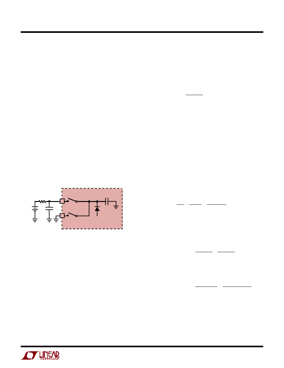
The equivalent input circuit is shown in Figure 1. Here, the
input is being driven by a resistive source, R
S
, with a
bypass capacitor, C
S
. The bypass capacitor may or may
not be needed, depending on the size of the source
resistance and the magnitude of the input voltage, V
IN
.
APPLICATIO S I FOR ATIO
W
U
U
U
Figure 1. Equivalent Input Circuit
V
IN
R
S
C
S
LTC1040 · AI01
S1
S2
C
IN
33pF
V
LTC1040 DIFFERENTIAL INPUT
+
For R
S
< 1Ok
Assuming C
S
is zero, the input capacitor, C
IN
, charges to
V
IN
with a time constant of R
S
C
IN
. When R
S
is too large,
C
IN
does not have a chance to fully charge during the
sampling interval (
80
µ
s) and errors will result. If R
S
exceeds 10k
, a bypass capacitor is necessary to mini-
mize errors.
For R
S
> 1Ok
For R
S
greater than 10k
, C
IN
cannot fully charge and a
bypass capacitor, C
S
, is needed. When switch S1 closes,
charge is shared between C
S
and C
IN
. The change in
voltage on C
S
because of this charge sharing is:
V = V
IN
·
C
IN
C
IN
+ C
S
R
IN
=
V
IN
I
IN
=
1
f
S
C
IN
=
1
f
S
· 33pF
This represents an error and can be made arbitrarily small
by increasing C
S
.
With the addition of C
S
, a second error term caused by the
finite input resistance of the LTC1040 must be considered.
Switches S1 and S2 alternately open and close, charging
and discharging C
IN
between V
IN
and ground. The
alternate charge and discharge of C
IN
causes a current to
flow into the positive input and out of the negative input.
The magnitude of this current is:
I
IN
= q · f
S
= V
IN
C
IN
f
S
where f
S
is the sampling frequency. Because the input
current is directly proportional to input voltage, the LTC1040
can be said to have an average input resistance of:
Notice that most of the error is caused by R
IN
. If the
sampling frequency is reduced to 1Hz, the voltage error is
reduced to 66
µ
V.
(see typical curve of Input Resistance vs Sampling Fre-
quency). A voltage divider is set up between R
S
and R
IN
causing error.
The input voltage error caused by these two effects is:
V
ERROR
= V
IN
Example: f
S
= 10Hz, R
S
= 1M
,
C
S
= 1
µ
F, V
IN
= 1V
(
)
C
IN
C
IN
+ C
S
+
R
S
R
S
+ R
IN
V
ERROR
= 1V
= 33
µ
V + 330
µ
V = 363
µ
V.
(
)
33 · 10
12
10
6
1 · 10
6
10
6
+ 3 · 10
9
+