 | –≠–ª–µ–∫—Ç—Ä–æ–Ω–Ω—ã–π –∫–æ–º–ø–æ–Ω–µ–Ω—Ç: LTC1043 | –°–∫–∞—á–∞—Ç—å:  PDF PDF  ZIP ZIP |

LTC1043
1
1043fa
Instrumentation Front End with 120dB CMRR
Precise, Charge-Balanced Switching
Operates from 3V to 18V
Internal or External Clock
Operates up to 5MHz Clock Rate
Low Power
Two Independent Sections with One Clock
The LTC
Æ
1043 is a monolithic, charge-balanced, dual
switched capacitor instrumentation building block. A pair
of switches alternately connects an external capacitor to
an input voltage and then connects the charged capacitor
across an output port. The internal switches have a
break-before-make action. An internal clock is provided
and its frequency can be adjusted with an external
capacitor. The LTC1043 can also be driven with an external
CMOS clock.
The LTC1043, when used with low clock frequencies,
provides ultra precision DC functions without requiring
precise external components. Such functions are
differential voltage to single-ended conversion, voltage
inversion, voltage multiplication and division by 2, 3, 4, 5,
etc. The LTC1043 can also be used for precise V≠F and
F≠V circuits without trimming, and it is also a building
block for switched capacitor filters, oscillators and
modulators.
The LTC1043 is manufactured using Linear Technology's
enhanced LTCMOS
TM
silicon gate process.
Dual Precision
Instrumentation Switched Capacitor
Building Block
, LTC and LT are registered trademarks of Linear Technology Corporation.
DESCRIPTIO
U
Precision Instrumentation Amplifiers
Ultra Precision Voltage Inverters, Multipliers
and Dividers
V≠F and F≠V Converters
Sample-and-Hold
Switched Capacitor Filters
Instrumentation Amplifier
CMRR vs Frequency
TYPICAL APPLICATIO
U
LTCMOS is a trademark of Linear Technology Corporation.
FREQUENCY OF COMMON MODE SIGNAL
100
20
CMRR (dB)
100
120
140
1k
10k
100k
LTC1043 ∑ TA02
80
60
40
C
S
= C
H
= 1µF
LTC1043 ∑ TA01
0.01
µ
F
≠5V
≠5V
5V
DIFFERENTIAL
INPUT
12
11
16
4
7
13
17
C
S
V
OUT
1
µ
F
C
H
1
µ
F
R2
R1
3
2
4
1
8
CMRR > 120dB AT DC
CMRR > 120dB AT 60Hz
DUAL SUPPLY OR SINGLE 5V
GAIN = 1 + R2/R1
V
OS
150
µ
V
2
µ
V/
∞
C
V
OS
T
COMMON MODE INPUT VOLTAGE INCLUDES THE SUPPLIES
1/2 LTC1043
5V
1/2 LTC1013
1
µ
F
(EXTERNAL)
8
14
≠
+
FEATURES
APPLICATIO S
U
LTC1043
2
1043fa
Supply Voltage ........................................................ 18V
Input Voltage at Any Pin .......... ≠ 0.3V V
IN
V
+
+ 0.3V
Operating Temperature Range
LTC1043C ................................... ≠ 40∞C T
A
85∞C
LTC1043M (OBSOLETE).............≠ 55∞C T
A
125∞C
Storage Temperature Range ................. ≠ 65∞C to 150∞C
Lead Temperature (Soldering, 10 sec).................. 300∞C
Consult LTC Marketing for parts specified with wider operating temperature ranges.
(Note 1)
ABSOLUTE AXI U RATI GS
W
W
W
U
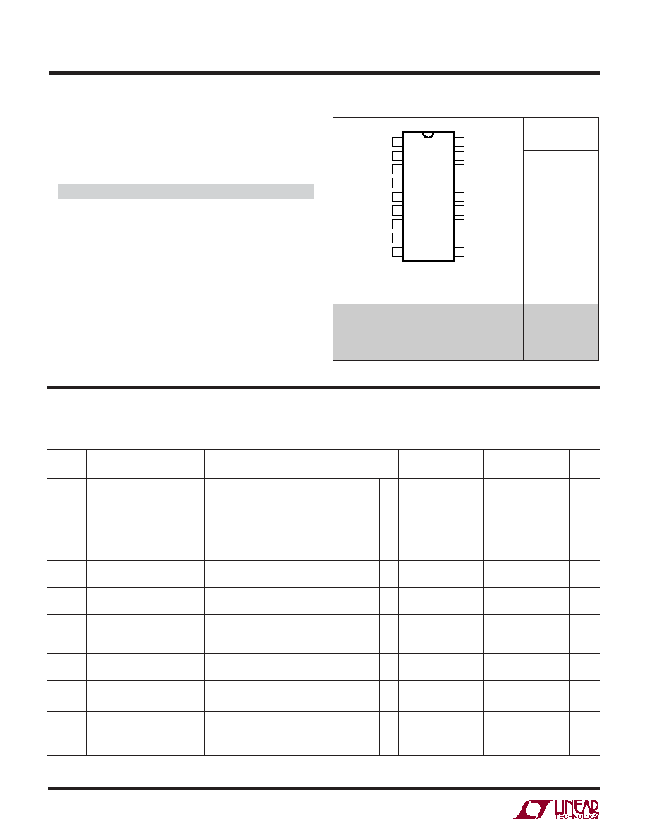
PACKAGE/ORDER I FOR ATIO
U
U
W
LTC1043M
LTC1043C
SYMBOL PARAMETER
CONDITIONS
MIN
TYP
MAX
MIN
TYP
MAX
UNITS
I
S
Power Supply Current
Pin 16 Connected High or Low
0.25
0.4
0.25
0.4
mA
0.7
0.7
mA
C
OSC
(Pin 16 to V
≠
) = 100pF
0.4
0.65
0.4
0.65
mA
1
1
mA
I
I
OFF Leakage Current
Any Switch, Test Circuit 1 (Note 2)
6
100
6
100
pA
6
500
6
nA
R
ON
ON Resistance
Test Circuit 2, V
IN
= 7V, 1 = ±0.5mA
240
400
240
400
V
+
= 10V, V
≠
= 0V
700
700
R
ON
ON Resistance
Test Circuit 2, V
IN
= 3.1V, 1 = ±0.5mA
400
700
400
700
V
+
= 5V, V
≠
= 0V
1
1
k
f
OSC
Internal Oscillator Frequency
C
OSC
(Pin 16 to V
≠
) = 0pF
185
185
kHz
C
OSC
(Pin 16 to V
≠
) = 100pF
20
34
50
20
34
50
kHz
Test Circuit 3
15
75
15
75
kHz
I
OSC
Pin Source or Sink Current
Pin 16 at V
+
or V
≠
40
70
40
70
µA
100
100
µA
Break-Before-Make Time
25
25
ns
Clock to Switching Delay
C
OSC
Pin Externally Driven
75
75
ns
f
M
Max External CLK Frequency
C
OSC
Pin Externally Driven with CMOS Levels
5
5
MHz
CMRR
Common Mode Rejection Ratio
V
+
= 5V, V
≠
= ≠ 5V, ≠5V < V
CM
< 5V
120
120
dB
DC to 400Hz
Note 1: Absolute Maximum Ratings are those values beyond which the life
of a device may be impaired.
ELECTRICAL CHARACTERISTICS
The
denotes specifications which apply over the full operating temperature
range, otherwise specifications are at T
A
= 25∞C. V
+
= 10V, V
≠
= 0V, LTC1043M operates from ≠55∞C T
A
125∞C; LTC1043C operates from
≠40∞C T
A
85∞C, unless otherwise noted.
Note 2: OFF leakage current is guaranteed but not tested at 25∞C.
ORDER PART
NUMBER
LTC1043CN
LTC1043CSW
LTC1043MD
LTC1043 ∑ POI01
1
2
3
4
5
6
7
8
9
18
17
16
15
14
13
12
11
10
SH
B
C
B
+
C
B
≠
V
+
S2B
S1B
S1A
S2A
NC
S3B
V
≠
C
OSC
S4B
S4A
S3A
C
A
≠
C
A
+
SH
A
N PACKAGE
18-LEAD PDIP
D PACKAGE
18-LEAD SIDE BRAZED (HERMETIC)
TOP VIEW
SW PACKAGE
18-LEAD PLASTIC SO
T
JMAX
= 100
∞
C,
JA
= 100
∞
C/W
PACKAGE (N)
T
JMAX
= 150
∞
C,
JA
= 85
∞
C/W PACKAGE (SW)
OBSOLETE PACKAGE
Consider the N18 Package as an Alternate Source

LTC1043
3
1043fa
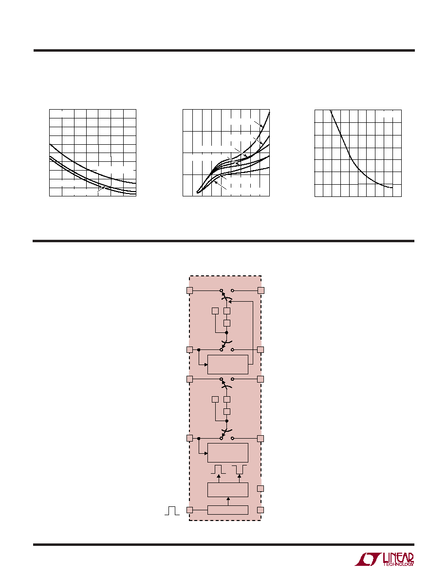
Power Supply Current vs
Power Supply Voltage
(Test Circuits 2 through 4)
TYPICAL PERFOR A CE CHARACTERISTICS
U
W
R
ON
vs V
IN
R
ON
vs V
IN
R
ON
vs V
IN
R
ON
(Peak) vs Power Supply
Voltage and Temperature
R
ON
(Peak) vs Power Supply
Voltage
Oscillator Frequency, f
OSC
vs C
OSC
Normalized Oscillator Frequency,
f
OSC
vs Supply Voltage
Oscillator Frequency, f
OSC
vs Supply Voltage
V
SUPPLY
(V)
0
SUPPLY CURRENT (mA)
1.6
1.4
1.2
1.0
0.8
0.6
0.4
0.2
0
16
LTC1043 ∑ TPC01
4
8
12
20
14
2
6
10
18
T
A
= ≠55∞C
C
OSC
= 0pF
C
OSC
= 0.0047pF
T
A
= 25∞C
C
OSC
= 0pF
C
OSC
= 0.0047pF
T
A
= 125∞C
C
OSC
= 0pF
C
OSC
= 0.0047pF
V
IN
(V)
0
R
ON
(
) 350
450
550
4
LTC1043 ∑ TPC02
250
150
300
400
500
200
100
1
2
3
5
V+ = 5V
V≠ = 0V
T
A
= 25
∞
C
V
IN
R
ON
(PEAK)
I = mA
I = 100
µ
A
I = 100
µ
A
V
IN
(V)
0
R
ON
(
) 180
220
260
16
LTC1043 ∑ TPC04
140
100
160
200
240
120
80
4
2
8
6
12 14
18
10
20
V+ = 15V
V≠ = 0V
T
A
= 25
∞
C
V
IN
R
ON
(PEAK)
I = mA
I = 100
µ
A
I = 100
µ
A
C
OSC
(pF)
1k
f
OSC
(Hz) 10k
100k
1M
0
4k
6k
8k
100
2k
10k
LTC1043 ∑ TPC07
T
A
= 25∞C
V+
= 15V, V≠ = 0V
V+
= 5V, V≠ = 0V
V+
= 10V, V≠ = 0V
V
SUPPLY
(V)
0
f
OSC
(kHz)
150
200
250
16
LTC1043 ∑ TPC08
100
50
125
175
225
75
25
4
2
8
6
12 14
18
10
20
T
A
= 25∞C
C
OSC
= 0pF
C
OSC
= 100pF
V
SUPPLY
(V)
0
NORMALIZED TO f
OSC
AT 5V SUPPLY
OSCILLATOR FREQUENCY
1.2
1.6
2.0
16
LTC1043 ∑ TPC09
0.8
0.4
1
1.4
1.8
0.6
0.2
0
4
2
8
6
12 14
18
10
20
0pF < C
OSC
< 0.01µF
T
A
= 25∞C
V
IN
(V)
0
R
ON
(
) 200
240
280
8
LTC1043 ∑ TPC03
160
120
220
260
180
140
100
2
4
6
10
7
1
3
5
9
V+ = 10V
V≠ = 0V
T
A
= 25
∞
C
V
IN
R
ON
(PEAK)
I = mA
I = 100
µ
A
I = 100
µ
A
V
SUPPLY
(V)
0
R
ON
(
) 600
800
1000
16
LTC1043 ∑ TPC05
400
200
500
700
900
300
100
0
4
2
8
6
12 14
18
10
20
V
IN
R
ON
(PEAK)
V
IN
= 1.6V
V
IN
3.2V
V
IN
7V
V
IN
11V
V
IN
15.1V
3V V+ + 18V
V≠ = 0V
T
A
= 25∞C
I = 100µA
V
SUPPLY
(V)
0
R
ON
(
) 700
900
1100
16
LTC1043 ∑ TPC06
500
300
600
800
1000
400
200
100
4
2
8
6
12 14
18
10
20
V
IN
R
ON
(PEAK)
T
A
= 125∞C
T
A
= ≠55∞C
I = 100µA
T
A
= 70∞C
LTC1043
4
1043fa
Oscillator Frequency, f
OSC
vs Ambient Temperature, T
A
(Test Circuits 2 through 4)
TYPICAL PERFOR A CE CHARACTERISTICS
U
W
Break-Before-Make Time, t
NOV
,
vs Supply Voltage
C
OSC
Pin I
SINK
, I
SOURCE
vs Supply Voltage
AMBIENT TEMPERATURE (∞C)
≠50
100
f
OSC
(kHz)
125
175
200
225
350
275
0
50
75
LTC1043 ∑ TPC10
150
300
325
250
≠25
25
100
125
C
OSC
= 0pF
V
+
= 10V, V
≠
= 0V
V
+
= 5V, V
≠
= 0V
V
+
= 15V, V
≠
= 0V
0
0
PIN 16 SOURCE OR SINK CURRENT (
µ
A)
25
50
75
100
2
4
6
8
LTC1043 ∑ TPC11
10
12
14
16
18
I
SINK,
T
A
= 25∞C
I
SOURCE,
T
A
= ≠55∞C
I
SOURCE,
T
A
= 25∞C
I
SINK,
T
A
= 125∞C
I
SOURCE,
T
A
= 125∞C
I
SINK,
T
A
= ≠55∞C
V
SUPPLY
(V)
0
10
t
NOV
(ns)
20
40
50
60
80
2
10
14
LTC1043 ∑ TPC12
30
70
8
18 20
4
6
12
16
T
A
= 25∞C
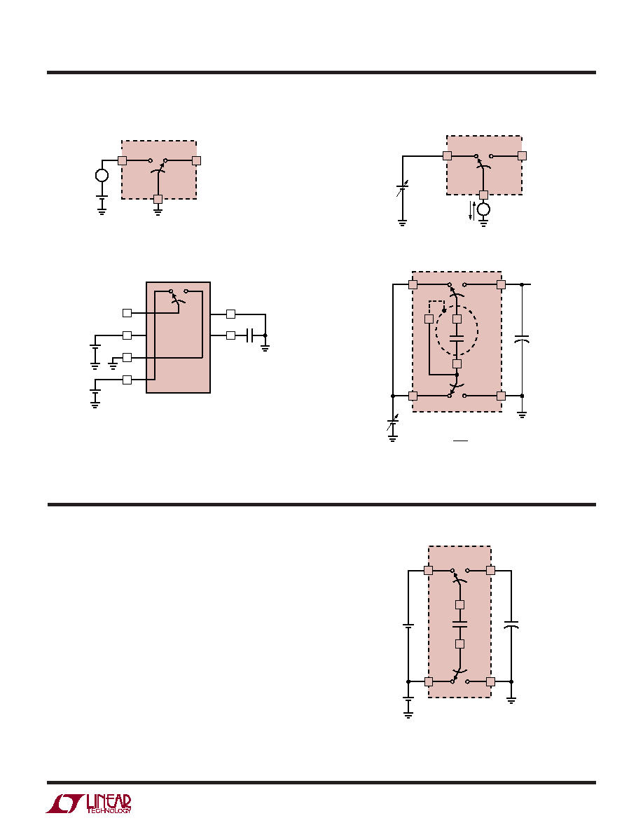
BLOCK DIAGRA
W
LTC1043 ∑ BD01
12
11
3
2
C
B
≠
C
B
+
SH
B
V
+
THE SWITCHES ARE TIMED AS SHOWN WITH PIN 16 HIGH
THE CHARGE BALANCING CIRCUITRY SAMPLES THE VOLTAGE
AT S3 WITH RESPECT TO S4 (PIN 16 HIGH) AND INJECTS A
SMALL CHARGE AT THE C
+
PIN (PIN 16 LOW).
THIS BOOSTS THE CMRR WHEN THE LTC1043 IS USED AS AN
INSTRUMENTATION AMPLIFIER FRONT END.
FOR MINIMUM CHARGE INJECTION IN OTHER TYPES OF
APPLICATIONS, S3A AND S3B SHOULD BE GROUNDED
V
≠
CHARGE
BALANCING
CIRCUITRY
NON-OVERLAPPING
CLOCK
OSCILLATOR
10
CHARGE
BALANCING
CIRCUITRY
1
C
A
≠
C
A
+
SH
A
C
OSC
S1A
7
13
6
18
16
4
17
8
14
15
5
S4A
S1B
S2B
S4B
V
+
V
≠
S2A
S3B
S3A
LTC1043
5
1043fa
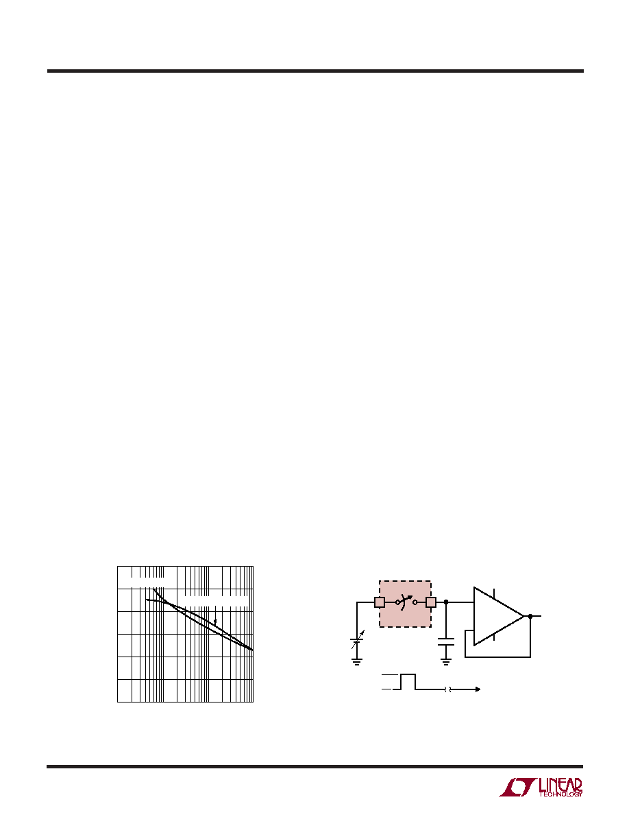
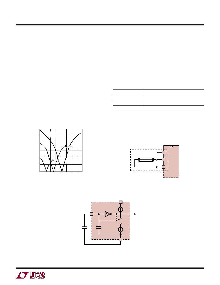
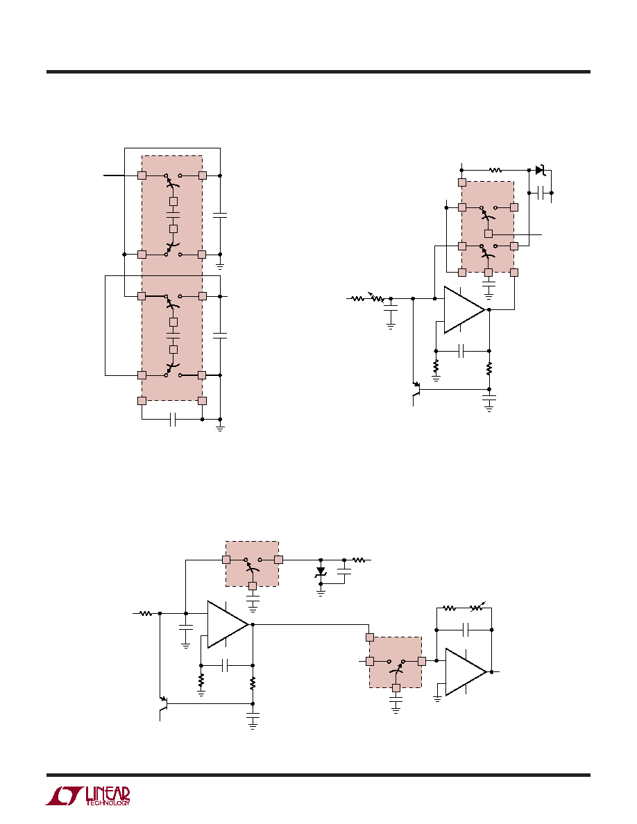
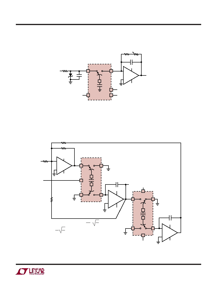
Test Circuit 1. Leakage Current Test
Common Mode Rejection Ratio (CMRR)
The LTC1043, when used as a differential to single-ended
converter rejects common mode signals and preserves
differential voltages (Figure 1). Unlike other techniques,
the LTC1043's CMRR does not degrade with increasing
common mode voltage frequency. During the sampling
mode, the impedance of Pins 2, 3 (and 11, 12) should be
reasonably balanced, otherwise, common mode signals
will appear differentially. The value of the CMRR depends
on the value of the sampling and holding capacitors
(C
S
, C
H
) and on the sampling frequency. Since the
common mode voltages are not sampled, the
common mode signal frequency can well exceed the
sampling frequency without experiencing aliasing
phenomena. The CMRR of Figure 1 is measured by
TEST CIRCUITS
Test Circuit 2. R
ON
Test
Test Circuit 3. Oscillator Frequency, f
OSC
Test Circuit 4. CMRR Test
LTC1043 ∑ TC02
(7, 13, 6, 18)
(8, 14, 5, 15)
(11, 12, 2, 3)
100µA to 1mA
CURRENT SOURCE
+
A
VIN
+
V+
LTC1043 ∑ TC03
4
V≠
16
(TEST PIN)
IV
5
LTC1043
17
C
OSC
2
+
6
LTC1043 ∑ TC04
CMRR = 20 LOG
( )
FOR OPTIMUM CMRR, THE C
OSC
SHOULD
BE LARGER THAN 0.0047µF, AND
THE SAMPLING CAPACITOR ACROSS
PINS 11 AND 12 SHOULD BE PLACED
OVER A SHIELD TIED TO PIN 10
+
V
≠
V
CM
V
+
V
CM
V
OUT
V
OUT
13
14
12
11
10
7
8
1µF
1µF
CAPACITORS ARE
NOT ELECTROLYTIC
NOTE:
+
APPLICATIO S I FOR ATIO
W
U
U
U
Figure 1. Differential to Single-Ended Converter
LTC1043 ∑ TC01
(7, 13, 6, 18)
(8, 14, 5, 15)
(11, 12, 2, 3)
NOTE: TO OPEN SWITCHES,
S1 AND S3
SHOULD BE CONNECTED
TO V≠. TO OPEN S2, S4,
C
OSC
PIN SHOULD BE
TO V+ C
OSC
+
A
0V TO 10V
LTC1043 ∑ AI01
C
S
, C
H
ARE MYLAR OR POLYSTRENE
+
C
H
C
S
C
≠
C
+
V
D
13
14
12
11
1/2 LTC1043
7
8
V
D
V
CM
+
+
LTC1043
6
1043fa
Figure 2. CMRR vs Sampling Frequency
Figure 3
APPLICATIO S I FOR ATIO
W
U
U
U
f
OSC
(Hz)
100
20
CMRR (dB)
100
120
140
1k
10k
100k
LTC1043 ∑ AI02
80
60
40
C
S
= C
H
= 1µF
C
S
= 1µF, C
ZH
= 0.1µF
LTC1043 ∑ AI03
1/8 LTC1043
6
V
OUT
V
IN
V
+
SAMPLE
HOLD TO PIN 16
0V
1000pF
5V
≠5V
≠
+
2
1/2 LTC1013
shorting Pins 7 and 13 and by observing, with a precision
DVM, the change of the voltage across C
H
with respect to
an input CM voltage variation. During the sampling and
holding mode, charges are being transferred and minute
voltage transients will appear across the holding capaci-
tor. Although the R
ON
on the switches is low enough to
allow fast settling, as the sampling frequency increases,
the rate of charge transfer increases and the average
voltage measured with a DVM across it will increase
proportionally; this causes the CMRR of the sampled data
system, as seen by a "continuous" instrument (DVM), to
decrease (Figure 2).
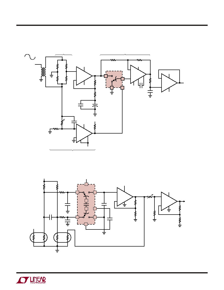
Switch Charge Injection
Figure 3 shows one out of the eight switches of the
LTC1043, configured as a basic sample-and-hold circuit.
When the switch opens, a ``hold step'' is observed and its
magnitude depends on the value of the input voltage.
Figure 4 shows charge injected into the hold capacitor. For
instance, a 2pCb of charge injected into a 0.01µF capacitor
causes a 200µV hold step. As shown in Figure 4, there is
a predictable and repeatable charge injection cancellation
when the input voltage is close to half the supply voltage
of the LTC1043. This is a unique feature of this product,
containing charge-balanced switches fabricated with a
self-aligning gate CMOS process. Any switch of the
LTC1043, when powered with symmetrical dual supplies,
will sample-and-hold small signals around ground with-
out any significant error.
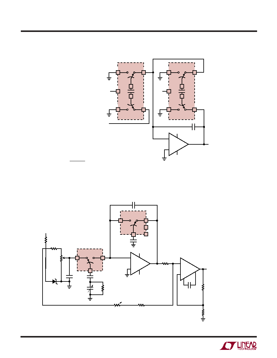
Shielding the Sampling Capacitor for Very High CMRR
Internal or external parasitic capacitors from the C
+
pin(s)
to ground affect the CMRR of the LTC1043 (Figure 1).
The common mode error due to the internal junction
capacitances of the C
+
Pin(s) 2 and 11 is cancelled through
internal circuitry. The C
+
pin, therefore, should be used as
the top plate of the sampling capacitor. The interpin
capacitance between pin 2 and dummy Pin 1 (11 and 10)
appears in parallel with the sampling capacitor so it does
not degrade the CMRR. A shield placed underneath
the sampling capacitor and connected to either Pin 1 or 3
helps to boost the CMRR in excess of 120dB (Figure 5).
Excessive external parasitic capacitance between the C
≠
pins and ground indirectly degrades CMRR; this becomes
visible especially when the LTC1043 is used with clock
frequencies above 2kHz. Because of this, if a shield is
used, the parasitic capacitance between the shield and
circuit ground should be minimized.
It is recommended that the outer plate of the sampling
capacitor be connected to the C
≠
pin(s).
Input Pins, SCR Sensitivity
An internal 60 resistor is connected in series with the
input of the switches (Pins 5, 6, 7, 8, 13, 14, 15, 18) and
it is included in the R
ON
specification. When the input
voltage exceeds the power supply by a diode drop, current
will flow into the input pin(s). The LTC1043 will not latch
until the input current reaches 2mA≠3mA. The device will
LTC1043
7
1043fa
Figure 4. Individual Switch Charge Injection
vs Input Voltage
Figure 5. Printed Circuit Board Layout
Showing Shielding the Sampling Capacitor
Figure 6. Internal Oscillator
APPLICATIO S I FOR ATIO
W
U
U
U
V
IN
(V)
0
0
CHARGE INJECTION (pCb)
2
4
6
8
4
8
12
16
LTC1043 ∑ AI04
10
12
2
6
10
14
V+ = 15V
V≠ = 0V
V+ = 10V
V≠ = 0V
V+ = 5V
V≠ = 0V
LTC1043 ∑ AI05
1
2
3
C
S
OUTSIDE FOIL
PRINTED CIRCUIT
BOARD AREA
LTC1043
recover from the latch mode when the input drops 3V to 4V
below the voltage value which caused the latch. For
instance, if an external resistor of 200 is connected in
series with an input pin, the input can be taken 1.3V above
the supply without latching the IC. The same applies for the
C
+
and C
≠
pins.
C
OSC
Pin (16), Figure 6
The Cosc pin can be used with an external capacitor, Cosc,
connected from Pin 16 to Pin 17, to modify the internal
oscillator frequency. If Pin 16 is floating, the internal 24pF
capacitor, plus any external interpin capacitance, set the
oscillator frequency around 190kHz with ±5V supply. The
typical performance characteristics curves provide the
necessary information to set the oscillator frequency for
various power supply ranges. Pin 16 can also be driven
with an external clock to override the internal oscillator.
Although standard 7400 series CMOS gates do not
guarantee CMOS levels with the current source and sink
requirements of Pin 16, they will in reality drive the Cosc
pin. CMOS gates conforming to standard B series output
drive have the appropriate voltage levels and more than
enough output current to simultaneously drive several
LTC1043 C
OSC
pins. The typical trip levels of the Schmitt
trigger (Figure 6) are given below.
LTC1043 * AI06
24pF
17
16
4
C
OSC
(EXTERNAL)
f
OSC
= 190kHz ∑
(24pF)
(24pF + C
OSC
)
C
OSC
V+
V≠
38µF
TO CLK GENERATOR
SUPPLY
TRIP LEVELS
V
+
= 5V, V
≠
= 0V
V
H
= 3.4VV
L
= 1.35V
V
+
= 10V, V
≠
= 0V
V
H
= 6.5VV
L
= 2.8V
V
+
= 15V, V
≠
= 0V
V
H
= 9.5VV
L
= 4.1V

LTC1043
8
1043fa
Divide by 2
Ultra Precision Voltage Inverter
Multiply by 2
Precision Multiply by 3
Divide by 3
Precision Multiply by 4
LTC1043 ∑ A01
0.01µF
V
OUT
=
V
IN
/2 ± 1ppm
0 V
IN
V
+
3 V+ 18V
12
11
7
13
V
OUT
= V
IN
/2
1µF
1µF
V
IN
1/2 LTC1043
8
14
16
17
LTC1043 ∑ A02
0.01µF
V
OUT
=
2V
IN
± 5ppm
0 V
IN
V
+
/2
3 V
+
18V
12
11
7
13
V
IN
1µF
1µF
V
OUT
1/2 LTC1043
8
14
16
17
LTC1043 * A03
0.01µF
V
OUT
=
≠V
IN
±2ppm
V
≠
< V
IN
<
V
+
V
+
= +5V, V
≠
= ≠5V
12
11
7
13
V
IN
1µF
1µF
V
OUT
= ≠V
IN
1/2 LTC1043
8
14
16
17
LTC1043 ∑ A04
0.01µF
V
OUT
=
3V
IN
±10ppm
0 < V
IN
<
V
+
/3
3V < V
+
< 18V
12
11
7
13
V
IN
V
OUT
1µF
1µF
LTC1043
8
14
16
17
3
2
1µF
5
15
1µF
6
18
LTC1043 ∑ A05
0.01µF
V
OUT
=
4V
IN
±40ppm
0 V
IN
V
+
/4
3V < V
+
< 18V
12
11
13
V
IN
2V
IN
V
OUT
= 4V
IN
1µF
1µF
LTC1043
8
14
16
3
2
1µF
5
15
1µF
6
18
7
17
LTC1043 ∑ A06
0.01µF
V
OUT
=
V
IN
/3
±3ppm
0 V
IN
V
+
12
11
7
13
V
IN
V
OUT
V
OUT
1µF
LTC1043
14
16
17
3
2
1µF
5
15
1µF
1µF
6
18
8
TYPICAL APPLICATIO S
U
LTC1043
9
1043fa
Divide by 4
0.005% V/F Converter
0.01% Analog Multiplier
LTC1043 ∑ A07
0.01µF
0
V
IN
V
+
V
OUT
= V
IN
/4 ±5ppm
12
11
V
OUT
V
IN
1µF
1µF
LTC1043
14
17
3
2
1µF
1µF
5
15
6
7
16
13
8
18
LTC1043 ∑ A08
≠5V
≠5V
30pF
22k
330k
1µF
Q1
2N2907A
5V
5V
≠5V
LT1009
2.5k
1µF
1k
f
OUT
: 0kHz TO 30kHz
7
8
13
V
IN
0V TO 3V
1µF
0.01µF
1/2 LTC1043
16
4
12
11
14
17
≠
+
6.19k
GAIN
2.5k
LF356
LTC1043 ∑ A09
0.001µF
1µF
1k
LT1004-1.2V
2N2907A
(FOR START-UP)
5V
X
INPUT
OPERATE LTC1043 FROM ±5V
POLYSTYRENE, MOUNT CLOSE
1% FILM RESISTOR
ADJUST OUTPUT TRIM
SO X ∑ Y = OUTPUT ±0.01%
Y
INPUT
1µF
1µF
2
3
4
6
7
1/4 LTC1043
12
14
5V
0.01µF
≠5V
2
3
4
7
6
≠
+
LT1056
≠5V
≠5V
≠5V
30pF
22k
330k
≠
+
LT1056
13
0.001µF
1/4 LTC1043
2
16
5
6
7.5k*
80.6k*
20k
OUTPUT
TRIM
OUTPUT
XY ±0.01%
*
TYPICAL APPLICATIO S
U

LTC1043
10
1043fa
Single 5V Supply, Ultra Precision
Instrumentation Amplifier
Precision Instrumentation Amplifier
Voltage Controlled Current Source with
Ground Referred Input and Output
LTC1043 ∑ A10
0.0047
INPUT AND OUTPUT VOLTAGE RANGE INCLUDES GROUND.
INPUT REFERRED OFFSET ERRORS ARE TYPICALLY 3µV WITH
1µV OF NOISE
CMRR ~ 120dB
12
11
7
13
INPUT
OUTPUT
A
V
= 1000
10k
1µF
1µF
100
43k
0.1µF 0.1µF
4
1
8
6
7
5V
3
2
LTC1043
14
16
4
3
2
1µF
1µF
NONPOLARIZED
5
15
1N914
5V
0.22µF
99.9k
6
18
8
+
≠
V
+
= 5V
≠
+
17
≠0.5V
~
LTC1052
LTC1043 ∑ A11
8
14
1µF
100
V
IN
100
INPUT
0V TO 2V
1
OUT
=
1/2 LTC1043
13
16
12
11
7
1k
4
1
8
5V
2
3
1µF
0.001µF
OPERATES FROM A SINGLE 5V SUPPLY
0.68µF
5V
4
≠
+
17
1/2 LT1013
LTC1043 ∑ A12
0.01µF
3
2
4
6
1µF
1µF
1µF
1M
CHOPPER
AC AMPLIFIER
PHASE
SENSITIVE
DEMODULATOR
DC
OUTPUT AMPLIFIER
1µF
100k
100k
100
100k
OUTPUT
0.01
R2
100k
R1
100
+ INPUT
≠ INPUT
1/2 LTC1043
5
15
16
5V
1µF
5V
≠5V
2
3
4
7
6
13
5V
≠5V
3
2
4
7
6
1/4 LTC1043
1/4 LTC1043
8
7
11
OFFSET = 10µV
DRIFT = 0.1µV/∞C
FULL DIFFERENTIAL INPUT
CMRR = 140dB
OPEN LOOP GAIN > 10
8
GAIN = R2/R1 + 1
I
BIAS
= 1nA
18
17
≠
+
LT1056
≠
+
LT1056
12
14
≠5V
TYPICAL APPLICATIO S
U
LTC1043
11
1043fa
Lock-In Amplifier (= Extremely Narrow-Band Amplifier)
50MHz Termal RMS/DC Converter
LTC1043 ∑ A013
13
1/4 LTC1043
T1 = TF5SX17ZZ, TOROTEL
R
T
= YSI THERMISTOR 44006
6.19k AT 37.5∞C
MATCH 0.05%
6.19k = VISHAY S-102
OPERATE LTC1043 WITH
±5V SUPPLIES
LOCK-IN AMPLIFIER TECHNIQUE
USED TO EXTRACT VERY SMALL
SIGNALS BURIED INTO NOISE
5V
≠5V
2
6.19k
100k
10k*
10k*
100
0.01µF
47µF
6.19k
1
4
3
6.19k
T1
500Hz
SINE DRIVE
THERMISTOR BRIDGE
IS THE SIGNAL SOURCE
SYNCHRONOUS
DEMODULATOR
RT
3
6
≠
+
LT1007
5V
5V
≠5V
ZERO CROSSING DETECTOR
2
3
4
1
8
1k
0.002
PHASE TRIM
50k
10k
7
5V
≠5V
30pF
3
2
1
8
1M
1µF
≠
+
LM301A
5V
≠5V
2
3
4
6
≠
+
LT1012
V
OUT
= 1000 ∑ DC
BRIDGE SIGNAL
12
14
16
≠
+
LT1011
*
+
LTC1043 ∑ A14
30k*
30k*
100k*
301*
10k
DC OUTPUT
0V TO 3.5V
10k
10k
RED
RED
T1B
*1% RESISTOR
T2B
1A
N
T2
T2A
GRN
300mV
10V
RMS
INPUT
0.01µF
GRN
BRN
CALIBRATION ADJUST
20k
5V
5V
5V
10k
10k
3
2
4
1
8
5
6
7
2% ACCURACY DC 50MHZ
100:1 CREST FACTOR CAPABILITY
T1 TO T2 = YELLOW SPRINGS INST. CO.
THERMISTOR COMPOSITE
ENCLOSE T1 AND T2 IN STYROFOAM
3
2
4
6
1µF
1µF
1µF
0.01µF
1µF
1/2 LTC1043
5
15
5V
18
17
16
≠
+
≠
+
LT1013
LT1013
TYPICAL APPLICATIO S
U
LTC1043
12
1043fa
Quad Single 5V Supply, Low Hold Step, Sample-and-Hold
Single Supply Precision Linearized Platinum RTD Signal Conditioner
LTC1043 ∑ A15
NC
OUTPUT
OUTPUT
NC
5V
2
3
11
4
1
11
7
8
V
IN
C
L
0.01µF
C
L
0.01µF
V
IN
6
5
7
12
13
14
≠
+
1/4 LT1014
≠
+
1/4 LT1014
≠ 5V
HOLD
SAMPLE
FOR 1V V
IN
4V, THE HOLD STEP IS 300µV
ACQUISITION TIME ~ 8 ∑ R
ON
C
H
FOR 10-BIT ACCURACY
LTC1043 ∑ A16
NC
OUTPUT
OUTPUT
NC
13
12
14
2
6
5
V
IN
C
L
0.01µF
C
L
0.01µF
9
10
8
3
18
15
16
17
4
≠
+
1/4 LT1014
≠
+
1/4 LT1014
V
IN
LTC1043 ∑ A17
887
1mA
R
p
= ROSEMOUNT 118MFRTD
1% FILM RESISTOR
TRIM SEQUENCE:
SET SENSOR TO 0∞C VALUE. ADJUST ZERO FOR 0V OUT
SET SENSOR TO 100∞C VALUE. ADJUST GAIN FOR 1,000V OUT
SET SENSOR TO 400∞C VALUE. ADJUST LINEARITY FOR 4,000V OUT
REPEAT AS REQUIRED
1µF
8.06k*
1k*
5k
0V TO 4V = 0∞C TO 400∞C
±0.05∞C
1µF
2k
R
p
100
AT 0∞C
12
11
7
1µF
0.1µF
1/2 LTC1043
8
14
13
5
1µF
1/2 LTC1043
6
18
16
5V
5V
250k*
(LINEARITY CORRECTION LOOP)
2.4k
2.74k*
8.25k*
50k
ZERO
ADJUST
LT1009
2.5V
10k*
3
2
4
1
8
5
6
7
1k
GAIN
ADJUST
≠
+
1/2 LT1013
≠
+
1/2 LT1013
4
15
17
0.01µF
3
2
*
TYPICAL APPLICATIO S
U
LTC1043
13
1043fa
High Frequency Clock Tunable Bandpass Filter
LTC1043 ∑ A18
≠5V
1k
≠5V
LT1004-1.2C
FREQUENCY IN
0kHz TO 30kHz
1µF
0V TO 3V OUTPUT
*75k = TRW # MTR-5/120ppm
≠5V
5V
1000pF
5V
1µF
75k*
1/4 LTC1043
12
14
13
≠
+
10k
GAIN TRIM
LF356
16
4
17
0.005% F/V Converter
1000pF
1000pF
12
11
7
200pF
1/2 LTC1043
8
14
13
R
Q
= 10k
BANDPASS CENTER FREQUENCY f
O
=
BANDPASS GAIN AT f
O
IS: R
Q
/R
IN
∑
f
O MAX
100kHz
Q
MAX
AT 100kHz f
O
IS 10
(f
O
∑ Q) MAX 1MHz
f
CLK MAX
3MHz, Q < 2
5V
≠5V
5V
5V
≠5V
≠ 5V
≠5V
≠
+
LT1056
LTC1043 ∑ A19
BANDPASS
OUTPUT
3
17
2
4
200pF
1/2 LTC1043
6
18
15
5V
5
16
≠
+
LT1056
≠
+
LT1056
V
IN
10k
R
IN
R1
10k
R2
10k
CLOCK
INPUT
Q =
R
Q
R2
R1
R2
f
CLK
31.4
R1
R2
TYPICAL APPLICATIO S
U
LTC1043
14
1043fa
Frequency-Controlled Gain Amplifier
LTC1043 ∑ A21
5V
≠5V
≠5V
2
3
4
6
7
≠
+
LT1056
3
10k
33k
22M
SENSOR
* = 1% FILM RESISTOR
LT1004
1.2V
500
90%
RH TRIM
10k
5% RH TRIM
2
1
100pF
9k*
1k*
SENSOR = PANAMETRICS # RHS
500pF AT RH = 76%
1.7 pF/%RH
6
8
≠
+
LM301A
OUTPUT
0V TO 1V = 0% TO 100%
1µF
100pF
0.01µF
1µF
1/4 LTC1043
12
1/4 LTC1043
11
8
7
16
17
14
13
1k*
470k
Relative Humidity Sensor Signal Conditioner
GAIN CONTROL
0kHz TO 10kHz = GAIN 0 TO 1000
0.01µF
1/2 LTC1043A
FOR DIFFERENTIAL INPUT, GROUND PIN 8A AND USE PINS 13A AND 7A FOR INPUTS
FOR SINGLE-ENDED INPUT AND POSITIVE GAIN, GROUND PIN 8A AND USE PIN 7A FOR INPUT
USE ± 5V SUPPLIES FOR LTC1043
5V
2
7
6
4
3
≠5V
LTC1043 ∑ A20
100pF
1/2 LTC1043B
f
IN
∑ 0.01µF
1kHz ∑ 100pF
≠
+
LT1056
V
IN
V
OUT
11A
11B
12B
12A
0.01µF
13A
14A
8A
7A
16A
13B
8B
7B
16B
14B
GAIN =
; GAIN IS NEGATIVE AS SHOWN
TYPICAL APPLICATIO S
U

LTC1043
15
1043fa
Linear Variable Differential Transformer (LVDT), Signal Conditioner
LTC1043 ∑ A23
0.01µF
12
SHUNT CAN BE IN POSITIVE
OR NEGATIVE SUPPLY LEAD
11
7
13
V
OUT
1µF
R
SHUNT
I
IN
1/2 LTC1043
8
14
16
17
1µF
+
Precision Current Sensing in Supply Rails
Information furnished by Linear Technology Corporation is believed to be accurate and reliable.
However, no responsibility is assumed for its use. Linear Technology Corporation makes no represen-
tation that the interconnection of its circuits as described herein will not infringe on existing patent rights.
LTC1043 ∑ A22
30k
0.005µF
30k
0.005µF
1/4 LTC1043
5
1µF
200k
OUTPUT
0V ±2.5V
0M 2.50M
10k GAIN TRIM
6
7
≠
+
1/2 LT1013
10k
100k
1.5kHz
4.7k
1.2k
Q1
2N4338
AMPLITUDE STABLE
SINE WAVE SOURCE
7.5k
100k
0.01µF
100k
PHASE
TRIM
10µF
LVDT = SCHAEVITZ E-100
1N914
LT1004
1.2V
5V
5V
≠ 5V
≠5V
5V
5V
1k
≠5V
LVDT
3
2
4
1
8
RD-BLUE
BLK
YEL-BLK
YEL-RED
BLUE
GRN
3
2
4
7
8
1
TO PIN 16, LTC1043
≠
+
LT1011
11
8
7
4
13
14
17
12
1/4 LTC1043
+
≠
+
LT1013
TYPICAL APPLICATIO S
U
LTC1043
16
1043fa
U
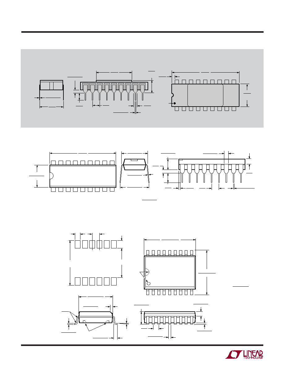
PACKAGE DESCRIPTIO
LW/TP 1202 1K REV A ∑ PRINTED IN USA
D Package
18-Lead Side Brazed (Hermetic)
(Reference LTC DWG # 05-08-1210)
N Package
18-Lead PDIP (Narrow .300 Inch)
(Reference LTC DWG # 05-08-1510)
Linear Technology Corporation
1630 McCarthy Blvd., Milpitas, CA 95035-7417
(408) 432-1900
FAX: (408) 434-0507
www.linear.com
LINEAR TECHNOLOGY CORPORATION 1985
S18 (WIDE) 0502
NOTE 3
.447 ≠ .463
(11.354 ≠ 11.760)
NOTE 4
15
14
13
12
11
10
16
9
N/2
1
2
3
4
5
6
7
8
.394 ≠ .419
(10.007 ≠ 10.643)
17
18
N
.037 ≠ .045
(0.940 ≠ 1.143)
.004 ≠ .012
(0.102 ≠ 0.305)
.093 ≠ .104
(2.362 ≠ 2.642)
.050
(1.270)
BSC
.014 ≠ .019
(0.356 ≠ 0.482)
TYP
0∞ ≠ 8∞ TYP
NOTE 3
.009 ≠ .013
(0.229 ≠ 0.330)
.016 ≠ .050
(0.406 ≠ 1.270)
.291 ≠ .299
(7.391 ≠ 7.595)
NOTE 4
◊ 45∞
.010 ≠ .029
(0.254 ≠ 0.737)
.420
MIN
.325 ±.005
RECOMMENDED SOLDER PAD LAYOUT
.045 ±.005
N
1
2
3
N/2
.050 BSC
.030 ±.005
TYP
.005
(0.127)
RAD MIN
INCHES
(MILLIMETERS)
NOTE:
1. DIMENSIONS IN
2. DRAWING NOT TO SCALE
3. PIN 1 IDENT, NOTCH ON TOP AND CAVITIES
ON THE BOTTOM OF PACKAGES ARE THE
MANUFACTURING OPTIONS.
THE PART MAY BE SUPPLIED WITH OR
WITHOUT ANY OF THE OPTIONS
4. THESE DIMENSIONS DO NOT INCLUDE
MOLD FLASH OR PROTRUSIONS.
MOLD FLASH OR PROTRUSIONS SHALL NOT
EXCEED .006" (0.15mm)
SW Package
18-Lead Plastic Small Outline (Wide .300 Inch)
(Reference LTC DWG # 05-08-1620)
N18 1002
.020
(0.508)
MIN
.120
(3.048)
MIN
.130 ± .005
(3.302 ± 0.127)
.065
(1.651)
TYP
.045 ≠ .065
(1.143 ≠ 1.651)
.018 ± .003
(0.457 ± 0.076)
.005
(0.127)
MIN
.255 ± .015*
(6.477 ± 0.381)
.900*
(22.860)
MAX
18
1
2
3
4
5
6
7
8
9
10
11
12
13
14
16
15
17
.008 ≠ .015
(0.203 ≠ 0.381)
.300 ≠ .325
(7.620 ≠ 8.255)
.325
+.035
≠.015
+0.889
≠0.381
8.255
(
)
NOTE:
1. DIMENSIONS ARE
INCHES
MILLIMETERS
*THESE DIMENSIONS DO NOT INCLUDE MOLD FLASH OR PROTRUSIONS.
MOLD FLASH OR PROTRUSIONS SHALL NOT EXCEED .010 INCH (0.254mm)
.100
(2.54)
BSC
OBSOLETE PACKAGE
.008 ≠ .015
(0.203 ≠ 0.381)
.300
(7.620)
REF
.485
(12.319)
MAX
.020 ≠ .060
(0.508 ≠ 1.524)
.015 ≠ .023
(0.381 ≠ 0.584)
.054
(1.372)
TYP
.100
(2.54)
BSC
.125
(3.175)
MIN
.165
(4.191)
MAX
D18 0801
1
8
2
7
3
6
4
5
.910
(23.114)
MAX
.290
(7.366)
TYP
9
10
11
12
13
14
15
16
.005
(0.127)
MIN
17
18
PIN NO. 1
IDENT