 | ÐлекÑÑоннÑй компоненÑ: LTC1045 | СкаÑаÑÑ:  PDF PDF  ZIP ZIP |
Äîêóìåíòàöèÿ è îïèñàíèÿ www.docs.chipfind.ru
1
LTC1045
Programmable
Micropower Hex Translator/
Receiver/Driver
100ns/DIV
045 TA01a
s
TTL/CMOS to
±
5V Analog Switch Drive
s
TTL to CMOS (3V to 15V V
CC
)
s
ECL to CMOS (3V to 15V V
CC
)
s
Ground Isolation Buffer
s
Low Power RS232 Line Receiver
APPLICATIO
N
S
U
TYPICAL APPLICATIO
N
U
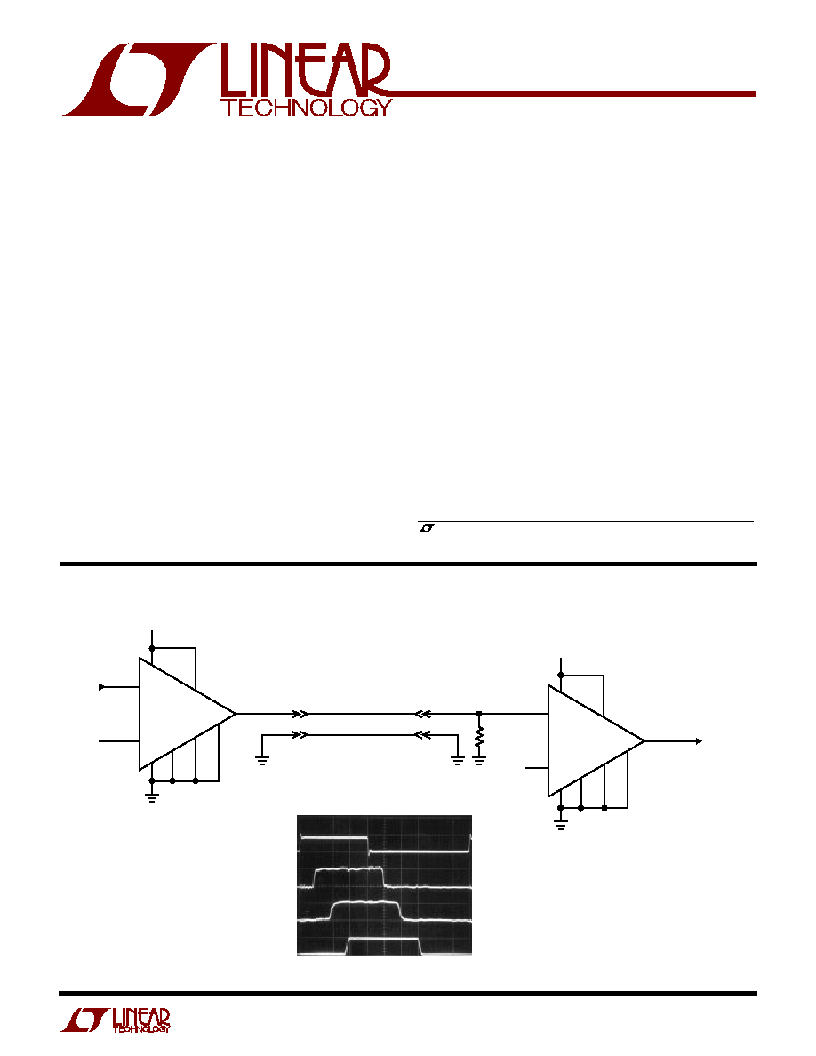
Flat Ribbon Cable Driver/Receiver
+
20
5V
11
1
TTL IN
1.4V
0.5V
XMT IN
XMT OUT
66-FT FLAT RIBBON CABLE
ADJACENT CONDUCTORS
Z
O
= 150
150
13
12
10
V
+
V
I
SET
DIS
V
OL
V
OH
RCV IN
1
RCV OUT
TTL OUT
1045 TA01
+
20
5V
11
13
12
10
V
+
V
I
SET
DIS
V
OL
V
OH
XMT IN (5V/DIV)
XMT OUT (1V/DIV)
RCV IN (1V/DIV)
RCV OUT (5V/DIV)
s
Efficiently Translate Voltage Levels
s
Internal Hysteresis for Noise Immunity
s
Output Latches Included
s
Three-State Outputs
s
Programmable Power/Speed
s
Power Can Be Completely Shut Off
s
±
50V on Inputs with External 100k Limit Resistor
s
1.2
µ
s Response at 100
µ
A Supply Current
FEATURES
The LTC
®
1045 is a hex level translator manufactured using
Linear Technology's enhanced LTCMOS
TM
silicon gate
process. It consists of six high speed comparators with
output latches and three-state capability. Each compara-
tor's plus input is brought out separately. The minus inputs
of comparators 1 to 4 are tied to V
TRIP1
while 5 and 6 are
tied to V
TRIP2
.
The I
SET
pin has several functions. When taken to V
+
the
outputs are latched and power is completely shut off.
Power/speed can be programmed by connecting I
SET
to V
through an external resistor.
DESCRIPTIO
N
U
, LTC and LT are registered trademarks of Linear Technology Corporation.
LTCMOS is a trademark of Linear Technology Corporation.
2
LTC1045
ORDER PART
NUMBER
Total Supply Voltage (V
+
, V
OH
to V
, V
OL
) .............. 18V
Output High Voltage (V
OH
) ......................................
V
+
Input Voltage ....................................18V to (V
0.3V)
Output Short-Circuit Duration
(V
OH
V
OL
10V) ................................... Continuous
ESD (MIL-STD-883, Method 3015) .................... 2000V
Operating Temperature Range ................. 40
°
C to 85
°
C
Storage Temperature Range ................. 55
°
C to 150
°
C
Lead Temperature (Soldering, 10 sec).................. 300
°
C
(Notes 1, 2)
ABSOLUTE
M
AXI
M
U
M
RATINGS
W
W
W
U
PACKAGE/ORDER I
N
FOR
M
ATIO
N
W
U
U
LTC1045CJ
LTC1045CN
LTC1045CSW
T
JMAX
= 150
°
C,
JA
= 70
°
C/ W (J)
T
JMAX
= 110
°
C,
JA
= 90
°
C/ W (N)
T
JMAX
= 110
°
C,
JA
= 90
°
C/ W (SW)
Consult factory for Industrial and Military grade parts.
ELECTRICAL CHARACTERISTICS
V
+
= V
OH
= 5V, V
= V
OL
= 0V, T
A
= 25
°
C, unless otherwise specified. (Note 3)
SYMBOL PARAMETER
CONDITIONS
MIN
TYP
MAX
UNITS
I
B
Input Bias Current
V
V
IN
V
+
±
1
nA
q
0.5
µ
A
Trip Voltage Range (Pins 8, 9)
q
V
V
+
2
V
I
S
V
+
to V
Supply Current
DISABLE = V
+
, R
SET
= 10k
2.5
3.5
mA
q
4.5
mA
I
OFF
V
+
to V
Supply Current in Shutdown
DISABLE = I
SET
= V
+
10
nA
q
1
µ
A
V
REF
Voltage on I
SET
(Pin 12)
R
SET
= 10k
0.9
V
q
0.6
1.25
V
V
OH
TTL Output High Voltage
I
OUT
= 360
µ
A, V
+
= 4.5V
q
2.4
4.4
V
V
OL
TTL Output Low Voltage
I
OUT
= 1.6mA, V
+
= 4.5V
q
0.2
0.4
V
I
SINK
Output Short-Circuit Sink Current
V
IN
= V
TRIP
100mV, V
OUT
= V
+
7.5
15
mA
q
5.5
mA
I
SOURCE
Output Short-Circuit Source Current
V
IN
= V
TRIP
+ 100mV, V
OUT
= V
4.0
8.0
mA
q
3.2
mA
I
OZ
Three-State Leakage Current
DISABLE = V
+
, V
OL
V
OUT
V
OH
0.005
µ
A
q
1
µ
A
R
OH
Output Resistance to V
OH
I
OUT
100
µ
A
260
475
q
600
R
OL
Output Resistance to V
OL
I
OUT
100
µ
A
100
180
q
250
I
SET
Voltage for Shutdown
q
V
+
0.5
V
DISABLE Input Logic Levels
V
IH
V
+
= 4.5V, V
= 0V
q
2.0
V
V
IL
V
+
= 5.5V, V
= 0V
q
0.8
V
Input Supply Differential
q
4.5
15
V
(V
+
V
) (Note 3)
Output Supply Differential
q
3
15
V
(V
OH
V
OL
) (Note 3)
1
2
3
4
5
6
7
8
9
10
TOP VIEW
J PACKAGE
20-LEAD CERDIP
N PACKAGE
20-LEAD PDIP
SW PACKAGE
20-LEAD SO WIDE
20
19
18
17
16
15
14
13
12
11
V
OH
IN1
IN2
IN3
IN4
IN5
IN6
V
TRIP2
V
TRIP1
V
V
+
OUT1
OUT2
OUT3
OUT4
OUT5
OUT6
DISABLE
I
SET
V
OL
3
LTC1045
The
q
denotes specifications which apply over the full operating
temperature range.
Note 1: Absolute Maximum Ratings are those values beyond which the life
of the device may be impaired.
Note 2: The maximum differential voltage between any two power pins
(V
+
, V
, V
OH
and V
OL
) must not exceed 18V. The maximum recommended
operating differential is 15V.
Note 3: During operation near the maximum supply voltage limit, care
should be taken to avoid or suppress power supply turn-on and turn-off
transients, power supply ripple or ground noise; any of these conditions
must not cause a supply differential to exceed the absolute maximum
rating.
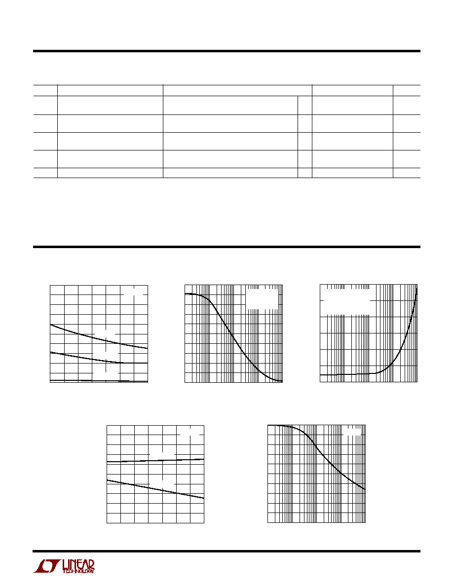
TYPICAL PERFOR
M
A
N
CE CHARACTERISTICS
U
W
I
+
vs Temperature
Delay Time vs R
SET
R
SET
(
)
5
4
3
2
1
0
100
10k
100k
1M
1045 G02
1k
V
+
TO V
CURRENT (mA)
T
A
= 25
°
C
V
+
= V
OH
= 5V
V
= V
OL
= 0V
I
+
vs R
SET
R
SET
(
)
DELAY TIME (
µ
s)
1.2
1.0
0.8
0.6
0.4
0.2
0
100
10k
100k
1M
1045 G03
1k
T
A
= 25
°
C
V
+
= V
OH
= 5V
V
= V
OL
= 0V
V
IN
= V
TRIP
±
100mV
V
REF
vs Temperature
TEMPERATURE (
°
C)
50
VOLTAGE ON I
SET
PIN (V)
2.5
2.0
1.5
1.0
0.5
0.1
25
0
75
100
1045 G04
25
50
125
V
+
= 5V
R
SET
= 10k
R
SET
= 1M
R
SET
(
)
20
18
16
14
12
10
8
6
4
2
0
100
10k
100k
1M
1045 G05
1k
COMPARATOR HYSTERESIS (mV)
V
+
= 5V
Hysteresis vs R
SET
TEMPERATURE (
°
C)
50
V
+
TO V
CURRENT (mA)
5
4
3
2
1
0
25
0
75
100
1045 G01
25
50
125
V
+
= 5V
R
SET
= 0
R
SET
= 10k
R
SET
= 1M
t
d
Response Time
Test Circuit Figure 1
250
ns
R
SET
= 10k,
±
100mV Drive
q
350
ns
t
SETUP
Time Before Rising Edge of I
SET
that
Test Circuit Figure 2
80
ns
Data Must Be Present
t
HOLD
Time After Rising Edge of I
SET
that
Test Circuit Figure 2
0
ns
Data Must Be Present
t
ACC
Falling Edge of DISABLE to Logic
Test Circuit Figure 3
165
ns
Level (from Hi-Z State)
t
IH
, t
OH
Rising Edge of DISABLE to Hi-Z State
Test Circuit Figure 3
200
ns
SYMBOL PARAMETER
CONDITIONS
MIN
TYP
MAX
UNITS
AC ELECTRICAL CHARACTERISTICS
V
+
= V
OH
= 5V, V
= V
OL
= 0V, T
A
= 25
°
C, unless otherwise specified.
4
LTC1045
V
OH
(Pin 1): High Level to which the Output Switches.
IN1 to IN7 (Pins 2 to 7): Six Comparator Inputs; Voltage
Range = V
to V
+ 18V.
V
TRIP2
(Pin 8): Trip Point for Last Two Comparators
(Inputs 5,6); Voltage Range = V
to V
+
2V.
V
TRIP1
(Pin 9): Trip Point for First Four Comparators
(Inputs 1 to 4); Voltage Range = V
to V
+
2V.
V
(Pin 10): Comparator Negative Supply.
V
OL
(Pin 11): Low Level to which the Output Switches.
I
SET
(Pin 12): This has three functions: 1) R
SET
from this
pin to V
sets bias current, 2) when forced to V
+
power is
shut off completely and 3) when forced to V
+
outputs are
latched.
DISABLE (Pin 13): When high, outputs are Hi-Z.
OUT6 to OUT1 (Pins 14 to 19): Six Driver Outputs.
V
+
(Pin 20): Comparator Positive Supply.
PI
N
FU
N
CTIO
N
S
U
U
U
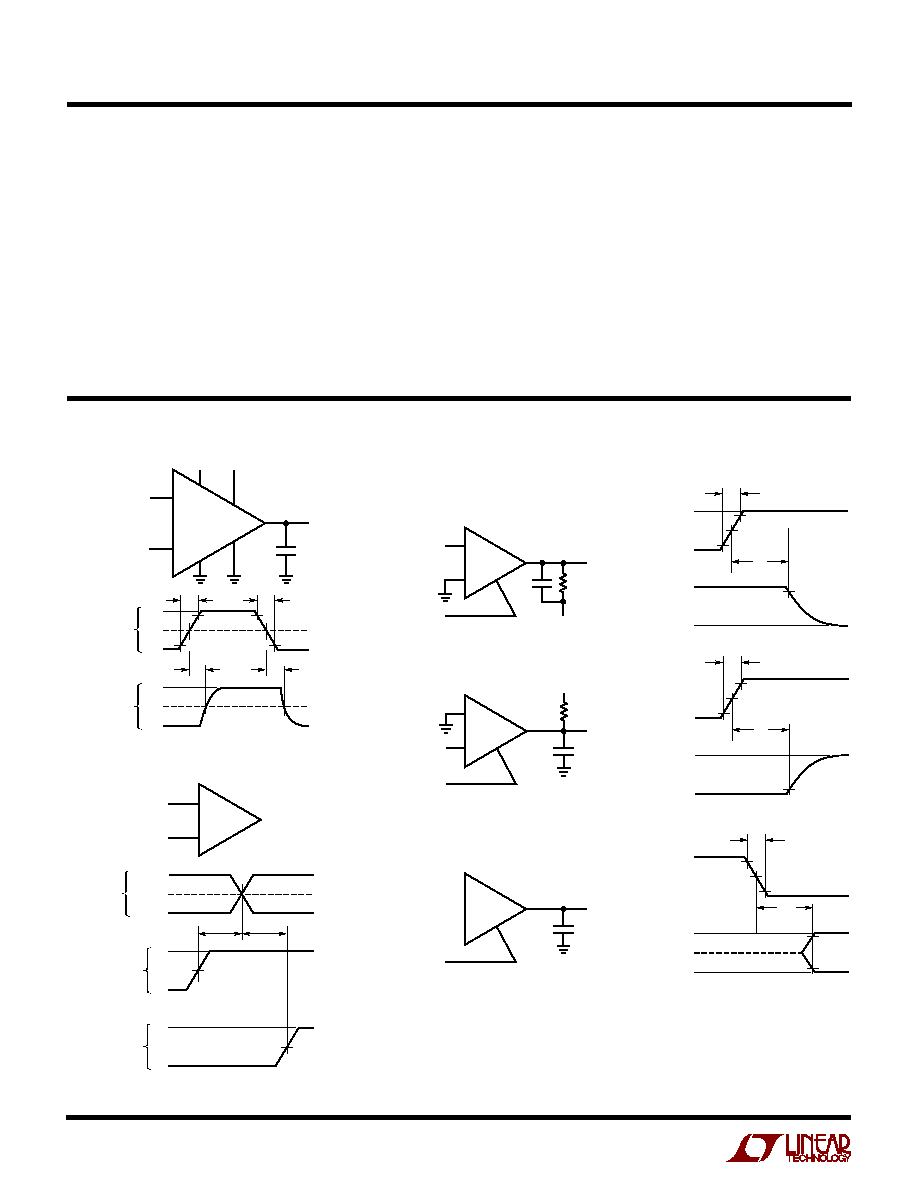
TEST CIRCUITS
50%
10%
90%
10%
t
OH
DISABLE
OUTPUTS
10pF
V
+
DISABLE
10k
V
OH
OUTPUT
1045 F03b
5V
5V
t
OH
t
r
10ns
50%
10%
90%
90%
t
IH
DISABLE
OUTPUTS
10pF
V
+
DISABLE
10k
V
OL
OUTPUT
1045 F03a
5V
5V
0V
5V
t
r
10ns
t
IH
+
50%
10%
90%
t
ACC
DISABLE
OUTPUTS
50pF
DISABLE
OUTPUT
1045 F03c
5V
5V
t
ACC
t
r
10ns
Figure 3. Three-State Output Test Circuit
Conditions: V
+
= V
OH
= 5V, V
= V
OL
= 0V
+
5V
5V
V
IN
V
TRIP
= 1.2V
V
+
V
V
OL
V
OH
OUTPUT
50pF
1045 F01
10%
t
r
= t
f
10ns
t
r
90%
90%
10%
V
IN
OUTPUT
1.3V
1.2V
1.1V
5V
2.5V
0V
t
d
t
f
t
d
50%
50%
1045 F02
V
IN
I
SET
100mV
V
TRIP
V
TRIP
= 1.2V
V
IN
100mV
5V
5V
0V
0V
t
HOLD
I
SET
t
SETUP
+
Figure 2. Latch Test Circuit
Figure 1. Response Time Test Circuit
5
LTC1045
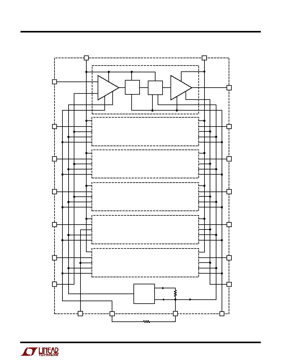
BLOCK DIAGRA
M
W
9
+
LEVEL
SHIFT
LATCH
V
+
V
V
BIAS
V
+
V
OH
V
OH
1
BIAS
GENERATOR
DISABLE
1045 BD
V
REF
1.6V
V
BIAS
SHUTDOWN
LATCH
ENABLE
8k
V
OL
13
11
V
TRIP1
V
TRIP2
8
OUT1
IN1
19
2
20
DIS
LE
V
OL
V
+
+
V
BIAS
V
V
OH
DIS
LE
V
OL
OUT2
IN2 3
18
V
+
+
V
BIAS
V
V
OH
DIS
LE
V
OL
OUT3
IN3 4
17
V
+
+
V
BIAS
V
V
OH
DIS
LE
V
OL
OUT4
IN4 5
16
V
+
+
V
BIAS
V
V
OH
DIS
LE
V
OL
OUT5
IN5 6
15
V
+
+
V
BIAS
V
V
OH
DIS
LE
V
OL
OUT6
IN6 7
14
I
SET
R
SET
12
V
10
9