 | ÐлекÑÑоннÑй компоненÑ: LTC1050 | СкаÑаÑÑ:  PDF PDF  ZIP ZIP |
1050fb.pm7
1
LTC1050
1050fb
+
7
8
13
14
16
17
11
4
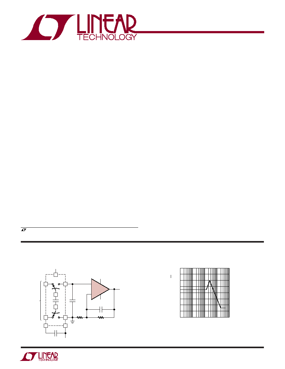
1/2 LTC1043
5V
C
S
1µF
C
H
1µF
DIFFERENTIAL
INPUT
12
0.01µF
R1
CMRR > 120dB AT DC
CMRR > 120dB AT 60Hz
DUAL SUPPLY OR SINGLE 5V
GAIN = 1 + R2/R1
V
OS
= 5µV
COMMON MODE INPUT VOLTAGE EQUALS THE SUPPLIES
R2
1050 TA01
5V
1µF
5V
5V
4
7
3
2
6
V
OUT
LTC1050
Precision Zero-Drift
Operational Amplifier
with Internal Capacitors
No External Components Required
Noise Tested and Guaranteed
Low Aliasing Errors
Maximum Offset Voltage: 5µV
Maximum Offset Voltage Drift: 0.05µV/°C
Low Noise: 1.6µV
P-P
(0.1Hz to 10Hz)
Minimum Voltage Gain: 130dB
Minimum PSRR: 125dB
Minimum CMRR: 120dB
Low Supply Current: 1mA
Single Supply Operation: 4.75V to 16V
Input Common Mode Range Includes Ground
Output Swings to Ground
Typical Overload Recovery Time: 3ms
The LTC
®
1050 is a high performance, low cost zero-drift
operational amplifier. The unique achievement of the
LTC1050 is that it integrates on-chip the two sample-and-
hold capacitors usually required externally by other chop-
per amplifiers. Further, the LTC1050 offers better com-
bined overall DC and AC performance than is available
from other chopper stabilized amplifiers with or without
internal sample-and-hold capacitors.
The LTC1050 has an offset voltage of 0.5µV, drift of
0.01µV/°C, DC to 10Hz, input noise voltage of 1.6µV
P-P
and a typical voltage gain of 160dB. The slew rate of 4V/µs
and a gain bandwidth product of 2.5MHz are achieved with
only 1mA of supply current.
Overload recovery times from positive and negative satu-
ration conditions are 1.5ms and 3ms respectively, which
represents an improvement of about 100 times over chop-
per amplifiers using external capacitors. Pin 5 is an optional
external clock input, useful for synchronization purposes.
The LTC1050 is available in standard 8-pin metal can,
plastic and ceramic dual-in-line packages as well as an
SO-8 package. The LTC1050 can be an improved plug-in
replacement for most standard op amps.
Thermocouple Amplifiers
Electronic Scales
Medical Instrumentation
Strain Gauge Amplifiers
High Resolution Data Acquisition
DC Accurate RC Active Filters
High Performance, Low Cost Instrumentation Amplifier
Noise Spectrum
FEATURES
DESCRIPTIO
U
APPLICATIO S
U
TYPICAL APPLICATIO
U
FREQUENCY (Hz)
40
VOLTAGE NOISE DENSITY (nV/
Hz)
80
100
140
160
10
1k
10k
100k
1050 TA02
0
100
120
60
20
, LTC and LT are registered trademarks of Linear Technology Corporation.
2
LTC1050
1050fb
ORDER PART
NUMBER
A
U
G
W
A
W
U
W
A
R
BSOLUTE
XI
TI
S
Operating Temperature Range
LTC1050AC/C .................................. 40°C to 85°C
LTC1050H ..................................... 40°C to 125°C
LTC1050AM/M (OBSOLETE) .......... 55°C to 125°C
Total Supply Voltage (V
+
to V
) .............................. 18V
Input Voltage ........................ (V
+
+ 0.3V) to (V
0.3V)
Output Short-Circuit Duration ......................... Indefinite
Storage Temperature Range ................ 65°C to 150°C
Lead Temperature (Soldering, 10 sec)................. 300°C
W
U
U
PACKAGE/ORDER I FOR ATIO
LTC1050ACH
LTC1050CH
LTC1050AMH
LTC1050MH
ORDER PART
NUMBER
1050
1050H
T
JMAX
= 150°C
(Note 1)
TOP VIEW
V
+
(CASE)
NC
NC
IN
OUT
EXT CLOCK
INPUT
+IN
V
8
7
6
5
3
2
1
4
H PACKAGE
8-LEAD TO-5 METAL CAN
S8 PART MARKING
LTC1050CS8
LTC1050HS8
1
2
3
4
8
7
6
5
TOP VIEW
NC
V
+
OUT
EXT CLOCK
INPUT
NC
IN
+IN
V
S8 PACKAGE
8-LEAD PLASTIC SO
+
T
JMAX
= 150°C,
JA
= 150°C/W
1
2
3
4
8
7
6
5
TOP VIEW
NC
IN
+IN
V
NC
V
+
OUT
EXT CLOCK
INPUT
N8 PACKAGE
8-LEAD PDIP
1
2
3
4
5
6
7
TOP VIEW
N PACKAGE
14-LEAD PDIP
14
13
12
11
10
9
8
NC
NC
NC
IN
+IN
NC
V
NC
NC
NC
V
+
OUT
NC
NC
T
JMAX
= 150°C,
JA
= 70°C/W
T
JMAX
= 150°C,
JA
= 100°C/W
ORDER PART
NUMBER
LTC1050ACN8
LTC1050CN8
ORDER PART
NUMBER
LTC1050CN
Consult LTC Marketing for parts specified with wider operating temperature ranges.
J8 PACKAGE 8-LEAD CERDIP
T
JMAX
= 150°C,
JA
= 100°C/W
LTC1050ACJ8
LTC1050CJ8
LTC1050AMJ8
LTC1050MJ8
OBSOLETE PACKAGE
OBSOLETE PACKAGE
ELECTRICAL C
C
HARA TERISTICS
LTC1050AM
LTC1050AC
PARAMETER
CONDITIONS
MIN
TYP
MAX
MIN
TYP
MAX
UNITS
Input Offset Voltage
(Note 3)
±0.5
±5
±0.5
±5
µV
Average Input Offset Drift
(Note 3)
±0.01
±0.05
±0.01
±0.05
µV/°C
Long Term Offset Voltage Drift
50
50
nV/Mo
Input Offset Current
(Note 5)
±20
±60
±20
±60
pA
±300
±150
pA
Input Bias Current
(Note 5)
±10
±30
±10
±30
pA
±2000
±100
pA
Input Noise Voltage
0.1Hz to 10Hz (Note 6)
1.6
2.1
1.6
2.1
µV
P-P
DC to 1Hz
0.6
0.6
µV
P-P
The
denotes specifications which apply over the full operating temperature
range, otherwise specifications are at T
A
= 25°C. V
S
= ±5V
Consider the N8 Package for Alternate Source
3
LTC1050
1050fb
ELECTRICAL C
C
HARA TERISTICS
LTC1050AM
LTC1050AC
PARAMETER
CONDITIONS
MIN
TYP
MAX
MIN
TYP
MAX
UNITS
Input Noise Current
f = 10Hz (Note 4)
1.8
1.8
fA/Hz
Common Mode Rejection Ratio
V
CM
= V
to 2.7V
114
140
114
140
dB
110
110
dB
Power Supply Rejection Ratio
V
S
= ±2.375V to ±8V
125
140
125
140
dB
Large-Signal Voltage Gain
R
L
= 10k, V
OUT
= ±4V
130
160
130
160
dB
Maximum Output Voltage Swing
R
L
= 10k
± 4.7
±4.85
±4.7
±4.85
V
R
L
= 100k
±4.95
±4.95
V
Slew Rate
R
L
= 10k, C
L
= 50pF
4
4
V/µs
Gain Bandwidth Product
2.5
2.5
MHz
Supply Current
No Load
1
1.5
1
1.5
mA
2.3
2.3
mA
Internal Sampling Frequency
2.5
2.5
kHz
The
denotes specifications which apply over the full operating temperature
range, otherwise specifications are at T
A
= 25°C. V
S
= ±5V
The
denotes specifications which apply over the full operating temperature range, otherwise specifications are at T
A
= 25°C.
V
S
= ±5V
LTC1050M/H
LTC1050C
PARAMETER
CONDITIONS
MIN
TYP
MAX
MIN
TYP
MAX
UNITS
Input Offset Voltage
(Note 3)
±0.5
±5
±0.5
±5
µV
Average Input Offset Drift
(Note 3)
±0.01
±0.05
±0.01
±0.05
µV/°C
Long Term Offset Voltage Drift
50
50
nV/Mo
Input Offset Current
(Note 5)
±20
±100
±20
±125
pA
±300
±200
pA
Input Bias Current
(Note 5)
±10
±50
±10
±75
pA
±2000
±150
pA
Input Noise Voltage
R
S
= 100, 0.1Hz to 10Hz (Note 6)
1.6
1.6
µV
P-P
R
S
= 100, DC to 1Hz
0.6
0.6
µV
P-P
Input Noise Current
f = 10Hz (Note 4)
1.8
1.8
fA/Hz
Common Mode Rejection Ratio
V
CM
= V
to 2.7V
114
130
114
130
dB
LTC1050M/C
110
110
dB
LTC1050H
100
dB
Power Supply Rejection Ratio
V
S
= ±2.375V to ±8V, LTC1050M/C
120
140
120
140
dB
LTC1050H
110
dB
Large-Signal Voltage Gain
R
L
= 10k, V
OUT
= ±4V
120
160
120
160
dB
Maximum Output Voltage Swing
R
L
= 10k
± 4.7
±4.85
±4.7
±4.85
V
R
L
= 100k
±4.95
±4.95
V
Slew Rate
R
L
= 10k, C
L
= 50pF
4
4
V/µs
Gain Bandwidth Product
2.5
2.5
MHz
Supply Current
No Load
1
1.5
1
1.5
mA
2.3
2.3
mA
Internal Sampling Frequency
2.5
2.5
kHz
Note 1: Absolute Maximum Ratings are those values beyond which the life
of the device may be impaired.
Note 2: Connecting any terminal to voltages greater than V
+
or less than
V
may cause destructive latchup. It is recommended that no sources
operating from external supplies be applied prior to power-up of the
LTC1050.
Note 3: These parameters are guaranteed by design. Thermocouple effects
preclude measurement of these voltage levels in high speed automatic test
systems. V
OS
is measured to a limit determined by test equipment
capability.
Note 4: Current Noise is calculated from the formula: In = (2q · Ib)
where q = 1.6 · 10
19
Coulomb.
Note 5: At T
A
0°C these parameters are guaranteed by design and not
tested.
Note 6: Every lot of LTC1050AM and LTC1050AC is 100% tested for
Broadband Noise at 1kHz and sample tested for Input Noise Voltage at
0.1Hz to 10Hz.
4
LTC1050
1050fb
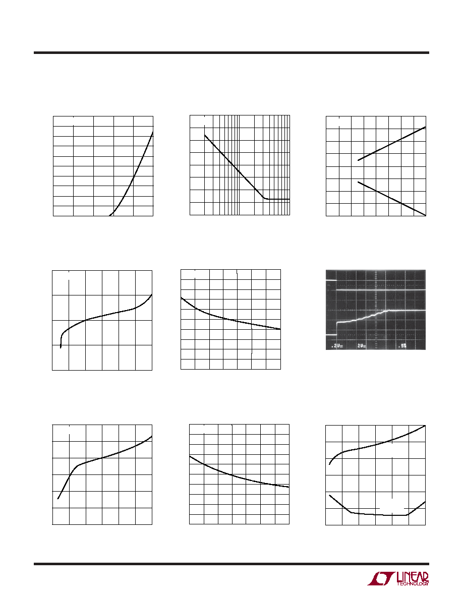
C
C
HARA TERISTICS
U
W
A
TYPICAL PERFOR
CE
Offset Voltage
vs Sampling Frequency
10Hz
P-P
Noise
vs Sampling Frequency
Common Mode Input Range
vs Supply Voltage
Supply Current vs Temperature
Supply Current vs Supply Voltage
Short-Circuit Output Current
vs Supply Voltage
SAMPLING FREQUENCY, f
S
(kHz)
2.0
OFFSET VOLTAGE (
µ
V)
6
8
10
4.0
1050 G01
4
2
0
2.5
3.0
3.5
4.5
V
S
= ± 5V
SAMPLING FREQUENCY, f
S
(Hz)
100
0
10Hz PEAK-TO-PEAK NOISE (
µ
V)
2
4
8
1k
10k
1050 G02
6
1
3
7
5
V
S
= ± 5V
SUPPLY VOLTAGE (V)
0
COMMON MODE RANGE (V)
0
4
± 8
1050 G03
4
8
± 2
± 4
± 6
±1
± 3
± 5
± 7
8
2
2
6
6
V
CM
= V
Sampling Frequency
vs Supply Voltage
Sampling Frequency
vs Temperature
Overload Recovery
TOTAL SUPPLY VOLTAGE, V
+
TO V
(V)
4
1.5
SAMPLING FREQUENCY, f
S
(kHz)
2.0
2.5
3.0
3.5
6
8
10
12
1050 G04
14
16
T
A
= 25°C
AMBIENT TEMPERATURE, T
A
(°C)
50
0
SAMPLING FREQUENCY, f
S
(kHz)
2
5
0
50
75
1050 G05
1
4
3
25
25
100
125
V
S
= ± 5V
TOTAL SUPPLY VOLTAGE, V
+
TO V
(V)
4
0
SUPPLY CURRENT, I
S
(mA)
0.25
0.50
0.75
1.00
1.50
6
8
10
12
1050 G07
14
16
1.25
T
A
= 25°C
AMBIENT TEMPERATURE, T
A
(°C)
50
0
SUPPLY CURRENT, I
S
(mA)
0.2
0.6
0.8
1.0
2.0
1.4
0
50
75
1050 G08
0.4
1.6
1.8
1.2
25
25
100
125
V
S
= ± 5V
TOTAL SUPPLY VOLTAGE, V
+
TO V
(V)
4
30
SHORT-CIRCUIT OUTPUT CURRENT, I
OUT
(mA)
20
10
0
2
6
6
8
10
12
1050 G09
14
16
4
I
SOURCE
V
OUT
= V
I
SINK
V
OUT
= V
+
200mV
0V
0V
5V
INPUT
OUTPUT
A
V
= 100
0.5ms/DIV
V
S
= ±5V
1050 G6
5
LTC1050
1050fb
C
C
HARA TERISTICS
U
W
A
TYPICAL PERFOR
CE
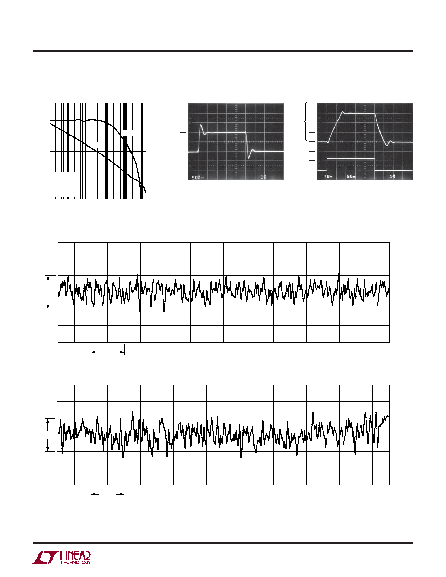
Gain/Phase vs Frequency
FREQUENCY (Hz)
0
VOLTAGE GAIN (dB)
PHASE SHIFT (DEGREES)
20
60
100
120
100
10k
100k
10M
1050 G10
20
1k
1M
80
40
40
180
160
120
80
60
200
100
140
220
PHASE
GAIN
V
S
= ± 5V
T
A
= 25°C
C
L
= 100pF
R
L
1k
Small-Signal Transient Response
Large-Signal Transient Response
LTC1050 DC to 1Hz Noise
0.5µV
10 SEC
1050 G13
LTC1050 DC to 10Hz Noise
1µV
1 SEC
1050 G14
100mV
STEP
A
V
= 1
R
L
= 10k
C
L
= 100pF
V
S
= ±5V
1050 G11
2V
A
V
= 1
R
L
= 10k
C
L
= 100pF
V
S
= ±5V
1050 G12
V
OUT
V
IN
= 6V