 | –≠–ª–µ–∫—Ç—Ä–æ–Ω–Ω—ã–π –∫–æ–º–ø–æ–Ω–µ–Ω—Ç: LTC1051 | –°–∫–∞—á–∞—Ç—å:  PDF PDF  ZIP ZIP |

1
LTC1051/LTC1053
10513fa
FREQUENCY (Hz)
10
VOLTAGE NOISE DENSITY (nV
Hz)
120
100
80
60
40
20
100
1k
10k
1051/53 TA01b
The LTC
Æ
1051/LTC1053 are high performance, low cost
dual/quad zero-drift operational amplifiers. The unique
achievement of the LTC1051/LTC1053 is that they integrate
on chip the sample-and-hold capacitors usually required
externally by other chopper amplifiers. Further, the
LTC1051/LTC1053 offer better combined overall DC and
AC performance than is available from other chopper
stabilized amplifiers with or without internal sample/hold
capacitors.
The LTC1051/LTC1053 have an offset voltage of 0.5µV,
drift of 0.01µV/∞C, DC to 10Hz, input noise voltage typically
1.5µV
P-P
and typical voltage gain of 140dB. The slew rate
of 4V/µs and gain bandwidth product of 2.5MHz are
achieved with only 1mA of supply current per op amp.
Overload recover times from positive and negative
saturation conditions are 1.5ms and 3ms respectively,
about a 100 or more times improvement over chopper
amplifiers using external capacitors.
The LTC1051 is available in an 8-lead standard plastic
dual-in-line package as well as a 16-pin SW package. The
LTC1053 is available in a standard 14-pin plastic package
and an 18-pin SO. The LTC1051/LTC1053 are plug in
replacements for most standard dual/quad op amps with
improved performance.
Thermocouple Amplifiers
Electronic Scales
Medical Instrumentation
Strain Gauge Amplifiers
High Resolution Data Acquisition
DC Accurate R C Active Filters
Dual/Quad Low Cost Precision Op Amp
No External Components Required
Maximum Offset Voltage: 5µV
Maximum Offset Voltage Drift: 0.05µV/∞C
Low Noise 1.5µV
P-P
(0.1Hz to 10Hz)
Minimum Voltage Gain: 120dB
Minimum PSRR: 120dB
Minimum CMRR: 114dB
Low Supply Current: 1mA/Op Amp
Single Supply Operation: 4.75V to 16V
Input Common Mode Range Includes Ground
Output Swings to Ground
Typical Overload Recovery Time: 3ms
Pin Compatible with Industry Standard Dual and
Quad Op Amps
Dual/Quad Precision
Zero-Drift Operational Amplifiers
With Internal Capacitors
High Performance Low Cost Instrumentation Amplifier
LTC1051 Noise Spectrum
≠
+
≠
+
5V
1/2
LTC1051
1/2
LTC1051
V
IN
V
IN
≠ 5V
R1
R2
R1
R2
1
2
3
4
5
6
7
8
1051/53 TA01a
R1 = 499, 0.1%
R2 = 100k, 0.1%
GAIN = 201
MEASURED CMRR ~ 120dB AT DC
MEASURED INPUT V
OS
3µV
MEASURED INPUT NOISE 2µV
P-P
(DC ≠ 10Hz)
FEATURES
DESCRIPTIO
U
TYPICAL APPLICATIO
U
, LTC and LT are registered trademarks of Linear Technology Corporation.
APPLICATIO S
U
LTC1051/LTC1053
2
10513fa
Total Supply Voltage (V
+
to V
≠
) ............................ 16.5V
Input Voltage ........................ (V
+
+ 0.3V) to (V
≠
≠ 0.3V)
Output Short-Circuit Duration .......................... Indefinite
Consult LTC Marketing for parts specified with wider operating temperature ranges.
(Note 1)
The
denotes the specifications which apply over the full operating
temperature range, otherwise specifications are at T
A
= 25∞C. V
S
= ±5V unless otherwise noted.
Operating Temperature Range
LTC1051M, LTC1051AM
(OBSOLETE) ..
≠55∞C to 125∞C
LTC1051C/LTC1053C ......................... ≠ 40∞C to 85∞C
Storage Temperature Range ................. ≠ 65∞C to 150∞C
Lead Temperature (Soldering, 10 sec).................. 300∞C
OBSOLETE PACKAGE
Consider the N8 Package as an Alternate Source
ABSOLUTE AXI U RATI GS
W
W
W
U
PACKAGE/ORDER I FOR ATIO
U
U
W
1
2
3
4
8
7
6
5
TOP VIEW
OUT A
≠ IN A
+IN A
V
≠
V
+
OUT B
≠IN B
+IN B
N8 PACKAGE
8-LEAD PDIP
J8 PACKAGE
8-LEAD CERDIP
ORDER PART
NUMBER
LTC1051CN8
LTC1051MJ8
LTC1051CJ8
LTC1051AMJ8
LTC1051ACJ8
ORDER PART
NUMBER
1
2
3
4
5
6
7
TOP VIEW
N PACKAGE
14-LEAD PDIP
14
13
12
11
10
9
8
OUT A
≠ IN A
+IN A
V
+
+IN B
≠ IN B
OUT B
OUT D
≠ IN D
+IN D
V
≠
+IN C
≠ IN C
OUT C
T
JMAX
= 150∞C,
JA
= 65∞C/W
LTC1053CN
1
2
3
4
5
6
7
8
TOP VIEW
SW PACKAGE
16-LEAD PLASTIC SO
16
15
14
13
12
11
10
9
NC
NC
OUT A
≠IN A
+IN A
V
≠
NC
NC
NC
NC
V
+
OUT B
≠IN B
+IN B
NC
NC
T
JMAX
= 150∞C,
JA
= 85∞C/W
T
JMAX
= 150∞C,
JA
= 90∞C/W
LTC1051CSW
LTC1053CSW
1
2
3
4
5
6
7
8
9
TOP VIEW
18
17
16
15
14
13
12
11
10
NC
OUT A
≠IN A
+IN A
V
+
+IN B
≠IN B
OUT B
NC
NC
OUT D
≠IN D
+IN D
V
≠
+IN C
≠IN C
OUT C
NC
SW PACKAGE
18-LEAD PLASTIC SO
T
JMAX
= 150∞C,
JA
= 110∞C/W
ORDER PART
NUMBER
ORDER PART
NUMBER
ELECTRICAL CHARACTERISTICS
LTC1051/LTC1053
LTC1051A
PARAMETER
CONDITIONS
MIN
TYP
MAX
MIN
TYP
MAX
UNITS
Input Offset Voltage
±0.5
±5
±0.5
±5
µV
Average Input Offset Drift
±0.0
±0.05
±0.0
±0.05
µV/∞C
Long Term Offset Drift
50
50
nV/Mo
Input Bias Current
±15
±65
±15
±50
pA
LTC1051C/LTC1053C
±135
±100
pA
Input Offset Current
(All Grades)
±30
±125
±30
±100
pA
±175
±150
pA
Input Noise Voltage (Note 2)
R
S
= 100, DC to 10Hz
1.5
1.5
2
µV
P-P
R
S
= 100, DC to 1Hz
0.4
0.4
µV
P-P

3
LTC1051/LTC1053
10513fa
The
denotes the specifications which apply over the full operating
temperature range, otherwise specifications are at T
A
= 25∞C. V
S
= ±5V unless otherwise noted.
ELECTRICAL CHARACTERISTICS
LTC1051/LTC1053
LTC1051A
PARAMETER
CONDITIONS
MIN
TYP
MAX
MIN
TYP
MAX
UNITS
Input Noise Current
f = 10Hz
2.2
2.2
fA/Hz
Common Mode Rejection Ratio, CMRR
V
CM
= V
≠
to 2.7V
106
130
114
130
dB
100
110
dB
Differential CMRR
V
CM
= V
≠
to 2.7V
112
112
dB
LTC1051, LTC1053 (Note 3)
Power Supply Rejection Ratio
V
S
= ±2.375V to ±8V
116
140
120
140
dB
Large Signal Voltage Gain
R
L
= 10k, V
OUT
= ±4V
116
160
120
160
dB
Maximum Output Voltage Swing
R
L
= 10k
±4.5
±4.85
±4.7
±4.85
V
R
L
= 100k
±4.5
±4.95
±4.95
V
Slew Rate
R
L
= 10k, C
L
= 50pF
4
4
V/µs
Gain Bandwidth Product
2.5
2.5
MHz
Supply Current/Op Amp
No Load
1
2
1
2
mA
2.5
2.5
mA
Internal Sampling Frequency
3.3
3.3
kHz
The
denotes the specifications which apply over the full operating temperature range, otherwise specifications are at T
A
= 25∞C.
V
S
= ±5V unless otherwise noted.V
S
= 5V, GND unless otherwise noted.
Note 1: Absolute Maximum Ratings are those values beyond which the life
of a device may be impaired.
Note 2: For guaranteed noise specification contact LTC Marketing.
Note 3: Differential CMRR for the LTC1053 is measured between
amplifiers A and D, and amplifiers B and C.
LTC1051A/LTC1051/LTC1053
PARAMETER
CONDITIONS
MIN
TYP
MAX
UNITS
Input Offset Voltage
±0.5
±5
µV
Input Offset Drift
±0.01
±0.05
µV/∞C
Input Bias Current
±10
±50
pA
Input Offset Current
±20
±80
pA
Input Noise Voltage
DC to 10Hz
1.8
µV
P-P
Supply Current/Op Amp
No Load
1.5
mA

LTC1051/LTC1053
4
10513fa
SUPPLY VOLTAGE (±V)
0
COMMON MODE RANGE (V)
1051/53 G01
1
2
3
4
5
6
7
8
8
6
4
2
0
≠ 2
≠ 4
≠ 6
≠ 8
V
CM
= V
≠
TOTAL SUPPLY VOLTAGE, V
+
TO V
≠
(V)
4
SAMPLING FREQUENCY, f
S
(kHz)
4.0
3.5
3.0
2.5
2.0
6
8
10
12
1051/53 G02
14
16
T
A
= 25∞C
AMBIENT TEMPERATURE, T
A
(∞C)
≠50
SAMPLING FREQUENCY, f
S
(kHz)
5
4
3
2
1
0
50
75
1051/53 G03
≠25
25
100
125
V
S
= ±5V
TOTAL SUPPLY VOLTAGE V
+
TO V
≠
(V)
4
SUPPLY CURRENT, I
S
(mA)
1.50
1.25
1.00
0.75
0.50
0.25
0
6
8
10
12
1051/53 G04
14
16
T
A
= 25∞C
AMBIENT TEMPERATURE, T
A
(∞C)
≠50
SUPPLY CURRENT, I
S
(mA)
2.0
1.8
1.6
1.4
1.2
1.0
0.8
0.6
0.4
0.2
0
0
50
75
1051/53 G05
≠25
25
100
125
V
S
= ±5V
FREQUENCY (Hz)
CMRR (dB)
160
140
120
100
80
60
40
20
0
1
100
1k
1051/53 G08
10
10k
100k
V
S
= ±5V
T
A
= 25∞C
AC COMMON MODE IN = 0.5V
P-P
Supply Current vs Supply Voltage
Per Op Amp
Output Short-Circuit Current vs
Supply Voltage
Common Mode Input Range vs
Supply Voltage
Sampling Frequency vs Supply
Voltage
Sampling Frequency vs
Temperature
Supply Current vs Temperature
Per Op Amp
Gain/Phase vs Frequency
CMRR vs Frequency
Gain/Phase vs Frequency
FREQUENCY (Hz)
VOLTAGE GAIN (dB)
120
100
80
60
40
20
0
≠ 20
≠ 40
100
10k
100k
10M
1051/53 G06
1k
1M
V
S
= ±5V
C
L
= 100pF
R
L
1k
T
A
= 25∞C
60
80
100
120
140
160
180
200
220
PHASE SHIFT (DEGREES)
TOTAL SUPPLY VOLTAGE, V
+
TO V
≠
(V)
4
SHORT-CIRCUIT OUTPUT CURRENT, I
OUT
(mA)
6
4
2
0
≠ 10
≠ 20
≠ 30
6
8
10
12
1051/53 G07
14
16
V
OUT
= V
≠
V
OUT
= V
+
I
SOURCE
I
SINK
TYPICAL PERFOR A CE CHARACTERISTICS
U
W
FREQUENCY (Hz)
VOLTAGE GAIN (dB)
120
100
80
60
40
20
0
≠ 20
≠ 40
100
10k
100k
10M
1051/53 G09
1k
1M
V
S
= ±2.5V
C
L
= 100pF
R
L
1k
T
A
= 25∞C
≠ 60
≠ 80
≠100
≠120
≠140
≠160
≠180
≠200
≠220
PHASE SHIFT (DEGREES)

5
LTC1051/LTC1053
10513fa
400mV
0
0
≠ 5V
INPUT
OUTPUT
1051/53 G10
A
V
= ≠100
V
S
= ±5V
0.5ms
10 SEC
1µV
1 SEC
V
S
= ±5V
T
A
= 25∞C
1.4µV
P-P
OUTPUT
50mV
/DIV
INPUT
100mV
2µs/DIV
A
V
= 1, R
L
= 10k, C
L
= 100pF
V
S
= ±5V, T
A
= 25∞C
1051/53 G11
OUTPUT
2V/DIV
INPUT
6V
2µs/DIV
A
V
= 1, R
L
= 10k, C
L
= 100pF
V
S
= ±5V, T
A
= 25∞C
1051/53 G12
Overload Recovery
Small Signal Transient Response
Large Signal Transient Response
LTC1051/LTC1053 DC to 10Hz Noise
≠
+
≠
+
1/2
LTC1051
LT1012
100k
158k
316k
475k
10
6
2
3
1051/53 TC01
≠
+
V
+
1/2
LTC1051
1M
1k
6
4
2
3
8
V
≠
R
L
OUTPUT
475k
TO X-Y
RECORDER
0.1µF
0.01µF
0.01µF
FOR 1Hz NOISE BW INCREASE ALL THE CAPACITORS BY A FACTOR OF 10.
Electrical Characteristics Test Circuit
DC 10Hz Noise Test Circuit
TYPICAL PERFOR A CE CHARACTERISTICS
U
W
TEST CIRCUITS

LTC1051/LTC1053
6
10513fa
ACHIEVING PICOAMPERE/MICROVOLT PERFORMANCE
Picoamperes
In order to realize the picoampere level of accuracy of the
LTC1051/LTC1053, proper care must be exercised. Leak-
age currents in circuitry external to the amplifier can
significantly degrade performance. High quality insulation
should be used (e.g., Teflon, Kel-F); cleaning of all insulat-
ing surfaces to remove fluxes and other residues will
probably be necessary --particularly for high temperature
performance. Surface coating may be necessary to provide
a moisture barrier in high humidity environments.
Board leakage can be minimized by encircling the input
connections with a guard ring operated at a potential close
to that of the inputs: in inverting configurations, the guard
ring should be tied to ground; in noninverting connections,
to the inverting input. Guarding both sides of the printed
circuit board is required. Bulk leakage reduction depends
on the guard ring width.
Microvolts
Thermocouple effects must be considered if the LTC1051/
LTC1053's ultra low drift op amps are to be fully utilized.
Any connection of dissimilar metals forms a thermoelec-
tric junction producing an electric potential which varies
with temperature (Seebeck effect.) As temperature sen-
sors, thermocouples exploit this phenomenon to produce
useful information. In low drift amplifier circuits, this effect
is a primary source of error.
Connectors, switches, relay contacts, sockets, resistors,
solder, and even copper wire are all candidates for thermal
EMF generation. Junctions of copper wire from different
manufacturers can generate thermal EMFs of 200nV/∞C--
4 times the maximum drift specification of the LTC1051/
LTC1053. The copper/kovar junction, formed when wire or
printed circuit traces contact a package lead, has a thermal
EMF of approximately 35µV/∞C--700 times the maximum
drift specification of the LTC1051/LTC1053.
Minimizing thermal EMF-induced errors is possible if
judicious attention is given to circuit board layout and
component selection. It is good practice to minimize the
number of junctions in the amplifier's input signal path.
Avoid connectors, sockets, switches and relays where
possible. In instances where this is not possible, attempt
to balance the number and type of junctions so that
differential cancellation occurs. Doing this may involve
deliberately introducing junctions to offset unavoidable
junctions.
When connectors, switches, relays and/or sockets are
necessary, they should be selected for low thermal EMF
activity. The same techniques of thermally balancing and
coupling the matching junctions are effective in reducing
the thermal EMF errors of these components.
Resistors are another source of thermal EMF errors.
Table 1 shows the thermal EMF generated for different
resistors. The temperature gradient across the resistor is
important, not the ambient temperature. There are two
junctions formed at each end of the resistor and if these
junctions are at the same temperature, their thermal EMFs
will cancel each other. The thermal EMF numbers are
approximate and vary with resistor value. High values give
higher thermal EMF.
Table 1. Resistor Thermal EMF
RESISTOR TYPE
THERMAL EMF/∞C GRADIENT
Tin Oxide
~mV/∞C
Carbon Composition
~450µV/∞C
Metal Film
~20µV/∞C
Wire Wound
Evenohm
~2µV/∞C
Manganin
~2µV/∞C
Input Bias Current, Clock Feedthrough
At ambient temperatures below 60∞C, the input bias cur-
rent of the LTC1051/LTC1053 op amps' is dominated by
the small amount of charge injection occurring during the
sampling and holding of the op amps' input offset voltage.
The average value of the resulting current pulses is 10pA
to 15pA with sign convention shown in Figure 1.
Figure 1. LTC1051 Bias Current
≠
+
≠
+
1/2
LTC1051
1/2
LTC1051
T
A
< 60∞C
T
A
> 85∞C
I
B
+
I
B
≠
I
B
+
I
B
≠
1051/53 F01
(a)
(b)
APPLICATIO S I FOR ATIO
W
U
U
U

7
LTC1051/LTC1053
10513fa
As the ambient temperature rises, the leakage current of
the input protection devices increases, while the charge
injection component of the bias current, for all practical
purposes, stays constant. At elevated temperatures (above
85∞C) the leakage current dominates and the bias current
of both inputs assumes the same sign.
The charge injection at the op amp input pins will cause
small output spikes. This phenomenon is often referred to
as "clock feedthrough" and can be easily observed when
the closed-loop gain exceeds 10V/V (Figure 2). The mag-
nitude of the clock feedthrough is temperature indepen-
dent but it increases when the closed-loop gain goes up,
when the source resistance increases and when the gain
setting resistors increase (Figure 2a, 2b). It is important to
note that the output small spikes are centered at 0V level
and do not add to the output offset error budget. For
instance, with R
S
= 1M, the typical output offset voltage
of Figure 2c is:
V
OS(OUT)
10
8
∑ I
B
+
+ 101V
OS(IN)
A 10pA bias current will yield an output of 1mV ±100µV.
The output clock feedthrough can be attenuated by lower-
ing the value of the gain setting resistors, i.e. R2 = 10k,
R1 = 100, instead of 100k and 1k (Figure 2).
Clock feedthrough can also be attenuated by adding a
capacitor across the feedback resistor to limit the circuit
bandwidth below the internal sampling frequency
(Figure 3).
Input Capacitance
The input capacitance of the LTC1051/LTC1053 op amps
is approximately 12pF. When the LTC1051/LTC1053 op
amps are used with feedback factors approaching unity,
the feedback resistor value should not exceed 7k for
industrial temperature range and 5k for military tempera-
ture range. If a higher feedback resistor value is required,
a feedback capacitor of 20pF should be placed across the
feedback resistor. Note that the most common circuits
with feedback factors approaching unity are unity gain
followers and instrumentation amplifier front ends.
(See Figure 4.)
Figure 2. Clock Feedthrough
Figure 3. Adding a Feedback Capacitor to
Eliminate Clock Feedthrough
≠
+
1/2
LTC1051
R
S
1051/53 F02
(c)
100µs/DIV
(b)
100µs/DIV
(a)
R1
1k
R2
100k
R
S
= 0,
A
V
=11V/V
20mV/DIV
R
S
= 0,
A
V
=101V/V
20mV/DIV
R
S
= 100k,
A
V
=11V/V
20mV/DIV
R
S
= 100k,
A
V
=101V/V
20mV/DIV
Figure 4. Operating the LTC1051
with Feedback Factors Approaching Unity
≠
+
1/2
LTC1051
1051/53 F04
R1
R2 < 7k, IF R1 > >R2
1
2
3
≠
+
1/2
LTC1051
R
S
1051/53 F03
R1
1k
R2
100k
C
1000pF
1
2
3
100µs/DIV
R
S
= 100k
A
V
=101V/V
R
S
= 1M
A
V
=101V/V
20mV/DIV
APPLICATIO S I FOR ATIO
W
U
U
U

LTC1051/LTC1053
8
10513fa
LTC1051/LTC1053 as AC Amplifiers
Although initially chopper stabilized op amps were de-
signed to minimize DC offsets and offset drifts, the
LTC1051/LTC1053 family, on top of its outstanding DC
characteristics, presents efficient AC performance. For
instance, at single 5V supply, each op amp typically
consumes 0.5mA and still provides 1.8MHz gain band-
width product and 3V/µs slew rate. This, combined with
almost distortionless swing to the supply rails (Figure 8),
makes the LTC1051/LTC1053 op amps nearly general
purpose. To further expand this idea (the "aliasing" phe-
nomenon) which can occur under AC conditions, should
be described and properly evaluated.
Aliasing
The LTC1051/LTC1053 are equipped with internal cir-
cuitry to minimize aliasing. Aliasing, no matter how small,
occurs when the input signal approaches and exceeds the
internal sampling rate. Aliasing is caused by the sampled
data nature of the chopper op amps. A generalized study
of this phenomenon is beyond the scope of a data sheet;
however, a set of rules of thumb can answer many
questions:
1. Alias signals can be generally defined as output AC
signals at a frequency of nf
CLK
± mf
IN
. The nf
CLK
term is the
internal sampling frequency of the chopper stabilized op
amps and its harmonics; mf
IN
is the frequency of the input
signal and its harmonics, if any.
≠
+
1/2
LTC1051
1051/53 F05a
R1
1k
R2
10k
1
2
3
f
IN
0.8V
P-P
0.1µF
0.1µF
50pF
5V
≠ 5V
V
OUT
B: MAG
RANGE: 9dBV
STATUS: PAUSED
RMS: 25
20dBV
15dB
/DIV
≠100
START: 100Hz
X: 1825Hz
BW: 47.742Hz
Y: ≠ 70.72dBV
STOP: 5 100Hz
f
IN
= 750Hz
f
CLK
≠ f
IN
2f
IN
2f
CLK
≠ f
IN
80dB
A: MAG
RANGE: 11dBV
STATUS: PAUSED
RMS: 25
20dBV
15dB
/DIV
≠100
CENTER: 10 000Hz
X: 5550Hz
BW: 95.485Hz
Y: ≠ 63.91dBV
SPAN: 10 000Hz
f
IN
= 10kHz
6f
CLK
≠ f
IN
74dB
Figure 5a. Output Voltage Spectrum of 1/2 LTC1051 Operating as an Inverting Amplifier with Gain of 10,
and Amplifying a 750Hz/800mV, Input AC Signal
Figure 5b. Same as Figure 5a, but the AC Input Signal is 900mV, 10kHz
APPLICATIO S I FOR ATIO
W
U
U
U
9
LTC1051/LTC1053
10513fa
2. If we arbitrarily accept that "aliasing" occurs when
output alias signals reach an amplitude of 0.01% or more
of the output signal, then: the approximate minimum
frequency of an AC input signal which will cause aliasing
is equal to the internal clock frequency multiplied by the
square root of the op amp feedback factor. For instance,
with closed-loop gain of ≠10, the feedback factor is 1/11
and if f
CLK
= 2.6kHz, alias signals can be detected when
the frequency of the input signal exceeds 750Hz to 800Hz
(Figure 5a).
3. The number of alias signals increases when the input
signal frequency increases (Figure 5b).
4. When the frequency, f
IN
, of the input signal is less than
f
CLOCK
, the alias signal(s) amplitude(s) directly scale with
the amplitude of the incoming signal. The output "signal to
alias ratio" cannot be increased by just boosting the input
signal amplitude. However, when the input AC signal
frequency well exceeds the clock frequency, the amplitude
of the alias signals does not directly scale with the input
amplitude. The "signal to alias ratio" increases when the
output swings closely to the rails. (See Figure 5b and
Figure 7.) It is important to note that the LTC1051/
LTC1053 op amps, under light loads (R
L
10k), swing
closely to the supply rails without generating harmonic
distortion (Figure 8).
B: MAG
RANGE: 9dBV
STATUS: PAUSED
RMS: 25
13dBV
15dB
/DIV
≠107
CENTER: 2 625Hz
X: 2535Hz
BW: 19.097Hz
Y: ≠ 74.16dBV
SPAN: 2 000Hz
f
IN
= 2.685kHz
f
CLK
2f
CLK
≠ f
IN
83.5dB
≠
+
1/2
LTC1051
1051/53 F05a
10k
10k
0.1µF
0.1µF
50pF
5V
≠ 5V
NOTE: THE f
CLK
≠ f
IN
= 85Hz
ALIAS FREQUENCY IS 95dB
DOWN FROM THE OUTPUT LEVEL
V
IN
= 10kHz
8V
P-P
Figure 6b. Output Voltage Spectrum of 1/2 LTC1051 Operating as a Unity-Gain Inverting Amplifier.
V
S
= ±5V, R
L
= 10k, C
L
= 50pF, V
IN
= 8V
P-P
, 10kHz
Figure 6a. Output Voltage Spectrum of 1/2 LTC1051 Operating as a Unity-Gain Inverting Amplifier.
V
S
= ±5V, R
L
= 10k, C
L
= 50pF, V
IN
= 8V
P-P
, 2.685kHz
B: MAG
RANGE: 9dBV
STATUS: PAUSED
RMS: 50
13dBV
15dB
/DIV
≠107
CENTER: 10 000Hz
X: 10000Hz
BW: 95.485Hz
Y: 7.98dBV
SPAN: 10 000Hz
f
IN
= 10kHz
f
IN
≠ f
CLK
2 ∑ f
CLK
6f
CLK
≠ f
IN
80dB
15dB
1kHz
5f
CLK
≠ f
IN
f
IN
≠ 2f
CLK
NOTE: ALL ALIAS FREQUENCY
80dB TO 84dB DOWN FROM OUTPUT
APPLICATIO S I FOR ATIO
W
U
U
U
LTC1051/LTC1053
10
10513fa
SYSTEM BUSY, ONLY ABORT COMMANDS ALLOWED
RANGE: 11dBV
STATUS: PAUSED
20dBV
15dB
/DIV
≠100
CENTER: 10 000Hz
X: 5475Hz
BW: 95.485Hz
Y: ≠58.05dBV
SPAN: 10 000Hz
f
IN
=10kHz
6f
CLK
≠ f
IN
68dB
≠
+
1/2
LTC1051
1051/53 F07
R1
100
R2
10k
90mV
P-P
10kHz
0.1µF
0.1µF
50pF
5V
≠ 5V
V
OUT
R
L
(LOAD RESISTANCE,)
V
OUT
±
SWING (
±
V)
1051/53 G08
0
1k 2k 3k
4k
5k
6k 7k
8k 9k 10k
NEGATIVE SWING
POSITIVE SWING
V
S
= ±8V, T
A
85∞C
V
S
= ±5V, T
A
85∞C
V
S
= ±2.5V, T
A
85∞C
10
9
8
7
6
5
4
3
2
1
0
INVERTING CLOSED-LOOP GAIN
1
OUTPUT SIGNAL TO ALIAS SIGNAL(S) RATIO (dB)
100
10
1051/53 G09
90
80
70
60
50
40
30
20
10
V
S
= ±5V
f
IN
10kHz
5. For unity-gain inverting configuration, all the alias
frequencies are 80dB to 84dB down from the output signal
(Figures 6a, 6b). Combined with excellent THD under wide
swing, the LTC1051/LTC1053 op amps make efficient
unity gain inverters.
For gain higher than ≠1, the "signal to alias" ratio de-
creases at an approximate rate of ≠6dB per decade of
closed-loop gain (Figure 9).
6. For closed-loop gains of ≠10 or higher, the "signal to
alias" ratio degrades when the value of the feedback gain
setting resistor increases beyond 50k. For instance, the
68dB value of Figure 7 decreases to 56dB if a (1k, 100k)
resistor set is used to set the gain of ≠100.
7. When the LTC1051/LTC1053 are used as noninverting
amplifiers, all the previous approximate rules of thumb
apply with the following exceptions: when the closed-loop
gain is 10(V/V) and below, the "signal to alias" ratio is 1dB
to 3dB less than the inverting case; when the closed-loop
gain is 100(V/V), the degradation can be up to 9dB,
especially when the input signal is much higher than the
clock frequency (i.e. f
IN
= 10kHz).
8. The signal/alias ratio performance improves when the
op amp has bandlimited loop gain.
Figure 7. Output Voltage Spectrum of 1/2 LTC1051 Operating as an Inverting Amplifier with a Gain of ≠100 and
Amplifiying a 90mV
P-P
, 10kHz Input Signal. With a 9V
P-P
Output Swing the Measured 2nd Harmonic (20kHz)
was 75 Down from the 10kHz Input Signal
Figure 8. Output Voltage Swing vs Load
Figure 9. Signal to Alias Ratio vs
Closed-Loop Gain
APPLICATIO S I FOR ATIO
W
U
U
U

11
LTC1051/LTC1053
10513fa
≠
+
≠
+
≠
+
A
B
1/2
LTC1051
1/2
LTC1051
A1
R1
R2
1
1
2
2
3
3
OUT
OUT
R3
R4
R5
C1
C2
5
6
6
7
8
5V
+
≠
1051/53 AC01a
A1
R1
R2
R3
R4
R5
C1
C2
e
OUT
(DC ≠ 1Hz)**
e
OUT
(DC ≠ 10Hz)**
LT1007
3k
2k
340k
10k
100k
0.01µF
0.001µF
0.1µV
P-P
0.15µV
P-P
LT1012*
750
57
250k
10k
100k
0.01µF
0.001µF
0.3µV
P-P
0.4µV
P-P
Obtaining Ultralow V
OS
Drift and Low Noise
The dual chopper op amp buffers the inputs of A1 and
corrects its offset voltage and offset voltage drift. With the
R, C values shown, the power-up warm up time is typically
20 seconds. The step response of the composite amplifier
does not present settling tails. The LT1007 should be used
when extremely low noise; V
OS
and V
OS
drift are sought
when the input source resistance is low--for instance a
350 strain gauge bridge. The LT1012 or equivalent
should be used when low bias current (100pA) is also
required in conjunction with DC to 10Hz low noise and low
V
OS
and V
OS
drift. The measured typical input offset
voltages were less than 2µV.
V
S
= ±5V
DC TO 10Hz
NOISE
1 SEC/DIV
0.2
µ
V/DIV
1051/53 AC01b
DC TO 1Hz
NOISE
LTC1051/LT1007 Peak-to-Peak Noise
TYPICAL APPLICATIO S
U
* Interchange connections A and B .
** Noise measured in a 10 sec window. Peak-to-peak noise was also measured for 10 continuous minutes: With the LT1007 op amp the recorded noise was less than 0.2µV
P-P
for both DC-1Hz
and DC-10Hz.
LTC1051/LTC1053
12
10513fa
+
≠
R1
R2
R
R
1/4
LTC1053
2
3
1
+
≠
R1
R2
R
1/4
LTC1053
+
≠
1/4
LTC1053
6
5
7
+
≠
R1
R2
R
1/4
LTC1053
9
10
13
12
14
4
11
8
V
IN
0.1µF
0.1µF
5V
≠5V
V
OUT
V
OUT
/ V
IN
= 3(R2/R1); INPUT DC ≠ 10Hz NOISE
0.8µV
P-P
= NOISE OF EACH PARALLELED OP AMP/3
NOTE: THIS CIRCUIT CAN ALSO BE USED AS A
DIFFERENCE AMPLIFIER FOR STRAIN GAUGES.
CONNECT R2/3 AND R1/3 FROM NONINVERTING
INPUTS, SHORTED TOGETHER, TO GROUND AND
TO SOURCE RESPECTIVELY.
1051/53 AC02
+
≠
≠
+
1/4
LTC1053
+
≠
1/4
LTC1053
+
≠
1/4
LTC1053
1/4
LTC1053
9
10
12
13
2
3
5
6
7
1
14
10k
10k
10k
10k
10k
20k
20k
10k
8
4
11
0.1µF
0.1µF
0.1µF
0.1µF
5V
≠5V
I
OUT
R
LOAD
1051/53 AC03
20k
10k
10k
R
G
V1
V2
∑ I
OUT
= 2(V2 ≠ V1)/R
G
∑ BW = 100Hz
∑
I
OUTMAX
= 1mA
≠
+
≠
+
≠
+
≠
+
5V
2
7
5
4
GND
LT1025A
R
≠
K
100
100
100
255k
0.068µF
255k
0.068µF
255k
0.068µF
0.1µF
0.1µF
0.1µF
1k
1k
1k
1/4
LTC1053
1/4
LTC1053
1/4
LTC1053
1/4
LTC1053
10k
10k
10k
10k
5V
ABSOLUTE
TEMPERATURE
ABSOLUTE
TEMPERATURE
OUTPUT
(DIFFERENTIAL
TEMPERATURE)
13
12
14
4
11
T
REF
TYPE K
+
≠
TYPE K
+
≠
TYPE K
+
≠
6
5
7
2
3
1
9
10
8
T2
T1
ALL FIXED RESISTORS ARE 1% METAL FILM
OUTPUT = T
REF
≠ T1 OR T
REF
≠ T2(10mV PER ∞C)
ACCURACY = (±0.1% FROM 25∞C TO 150∞C)
1051/53 AC04
S1
Paralleling Choppers to Improve Noise
Differential Voltage to Current Converter
Multiplexed Differential Thermometer
TYPICAL APPLICATIO S
U
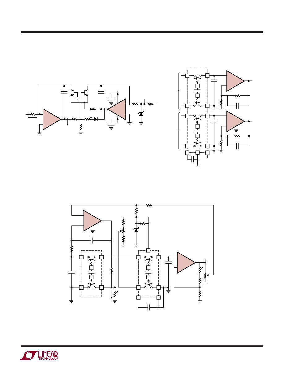
13
LTC1051/LTC1053
10513fa
≠
+
≠
+
0.1µF
0.1µF
1/2
LTC1051
1/2
LTC1051
Q1
Q1
0.0022µF
22pF
10k
0.1%
1k
0.1%
V
IN
1nA < I
IN
<1mA
V
OUT
=
LOG V
IN
≠2V
2M
15.8k
0.1%
3k
0.1%
1N4148
5V
5V
2.5V
≠5V
1
2
3
4
5
6
7
8
2.5M
0.1%
LT1009
Q1: TEL LAB TYPE Q81
ADJUST 2M POR. FOR NONLINEARITIES
1051/53 AC05
Six Decade Log Amplifier
Dual Instrumentation Amplifier
Linearized Platinum Signal Conditioner
≠
+
1/2
LTC1051
5
6
7
5V
1µF
1µF
≠
+
1/2
LTC1051
3
2
1
5V
8
4
6
5
2
3
4
18
17
16
1µF
7
11
12
14
13
0.01µF
1k
GAIN
ADJUST
5k
1k
8.06k*
0V TO 4V =
0∞C TO 400∞C
±0.05∞C
8.25k*
274k*
10k*
50k
ZERO
ADJUST
250k*
LT1009
2.5V
2.4k
RP = ROSEMOUNT 118MFRTD
*1% FILM RESISTOR
TRIM SEQUENCE:
SET SENSOR TO 0∞C VALUE. ADJUST ZERO FOR 0V OUT
SET SENSOR TO 100∞C VALUE. ADJUST GAIN FOR 1.000V OUT
SET SENSOR TO 400∞C VALUE. ADJUST LINEARITY FOR 4.000V OUT
REPEAT AS REQUIRED. FOR MORE INFORMATION REFER TO AN3
15
887
1µF
0.1µF
2k
1/2 LTC1043
1/2 LTC1043
R
P
100
AT 0∞C
I
K
1051/53 AC07
(LINEARITY CORRECTION LOOP)
8
≠
+
1/2
LTC1051
3
2
1
1k
0.22µF
100k
5V
5V
V
OUT1
V
OUT2
1µF
1µF
≠
+
1/2
LTC1051
5
6
7
4
8
1k
0.22µF
0.0047µF
100k
1µF
8
7
11
12
14
13
1µF
5
6
2
3
17
15
18
4
16
≠
+
≠
+
INPUT 1
INPUT 2
GAIN = 101V/DIV
CMRR >100dB
V
OS
3µV
INPUT REFERRED NOISE 2µV
P-P
1051/53 AC06
LTC1043
TYPICAL APPLICATIO S
U

LTC1051/LTC1053
14
10513fa
J Package
8-Lead CERDIP (Narrow 0.300, Hermetic)
(LTC DWG # 05-08-1110)
N Package
8-Lead PDIP (Narrow 0.300)
(LTC DWG # 05-08-1510)
N Package
14-Lead PDIP (Narrow 0.300)
(LTC DWG # 05-08-1510)
J8 0801
.014 ≠ .026
(0.360 ≠ 0.660)
.015 ≠ .060
(0.381 ≠ 1.524)
.125
3.175
MIN
.100
(2.54)
BSC
.300 BSC
(7.62 BSC)
.008 ≠ .018
(0.203 ≠ 0.457)
0∞ ≠ 15∞
.045 ≠ .065
(1.143 ≠ 1.651)
.045 ≠ .068
(1.143 ≠ 1.650)
FULL LEAD
OPTION
.023 ≠ .045
(0.584 ≠ 1.143)
HALF LEAD
OPTION
CORNER LEADS OPTION
(4 PLCS)
.200
(5.080)
MAX
.005
(0.127)
MIN
.405
(10.287)
MAX
.220 ≠ .310
(5.588 ≠ 7.874)
1
2
3
4
8
7
6
5
.025
(0.635)
RAD TYP
NOTE: LEAD DIMENSIONS APPLY TO SOLDER
DIP/PLATE OR TIN PLATE LEADS
OBSOLETE PACKAGE
U
PACKAGE DESCRIPTIO
N8 1002
.065
(1.651)
TYP
.045 ≠ .065
(1.143 ≠ 1.651)
.130 ± .005
(3.302 ± 0.127)
.020
(0.508)
MIN
.018 ± .003
(0.457 ± 0.076)
.120
(3.048)
MIN
1
2
3
4
8
7
6
5
.255 ± .015*
(6.477 ± 0.381)
.400*
(10.160)
MAX
.008 ≠ .015
(0.203 ≠ 0.381)
.300 ≠ .325
(7.620 ≠ 8.255)
.325
+.035
≠.015
+0.889
≠0.381
8.255
(
)
.100
(2.54)
BSC
NOTE:
1. DIMENSIONS ARE
*THESE DIMENSIONS DO NOT INCLUDE MOLD FLASH OR PROTRUSIONS.
MOLD FLASH OR PROTRUSIONS SHALL NOT EXCEED .010 INCH (0.254mm)
INCHES
MILLIMETERS
N14 1002
.008 ≠ .015
(0.203 ≠ 0.381)
.300 ≠ .325
(7.620 ≠ 8.255)
.325
+.035
≠.015
+0.889
≠0.381
8.255
(
)
.255 ± .015*
(6.477 ± 0.381)
.770*
(19.558)
MAX
3
1
2
4
5
6
7
8
9
10
11
12
13
14
NOTE:
1. DIMENSIONS ARE
INCHES
MILLIMETERS
*THESE DIMENSIONS DO NOT INCLUDE MOLD FLASH OR PROTRUSIONS.
MOLD FLASH OR PROTRUSIONS SHALL NOT EXCEED .010 INCH (0.254mm)
.020
(0.508)
MIN
.120
(3.048)
MIN
.130 ± .005
(3.302 ± 0.127)
.045 ≠ .065
(1.143 ≠ 1.651)
.065
(1.651)
TYP
.018 ± .003
(0.457 ± 0.076)
.005
(0.125)
MIN
.100
(2.54)
BSC
15
LTC1051/LTC1053
10513fa
Information furnished by Linear Technology Corporation is believed to be accurate and reliable.
However, no responsibility is assumed for its use. Linear Technology Corporation makes no represen-
tation that the interconnection of its circuits as described herein will not infringe on existing patent rights.
S18 (WIDE) 0502
NOTE 3
.447 ≠ .463
(11.354 ≠ 11.760)
NOTE 4
15
14
13
12
11
10
16
9
N/2
1
2
3
4
5
6
7
8
.394 ≠ .419
(10.007 ≠ 10.643)
17
18
N
.037 ≠ .045
(0.940 ≠ 1.143)
.004 ≠ .012
(0.102 ≠ 0.305)
.093 ≠ .104
(2.362 ≠ 2.642)
.050
(1.270)
BSC
.014 ≠ .019
(0.356 ≠ 0.482)
TYP
0∞ ≠ 8∞ TYP
NOTE 3
.009 ≠ .013
(0.229 ≠ 0.330)
.016 ≠ .050
(0.406 ≠ 1.270)
.291 ≠ .299
(7.391 ≠ 7.595)
NOTE 4
◊ 45∞
.010 ≠ .029
(0.254 ≠ 0.737)
.420
MIN
.325 ±.005
RECOMMENDED SOLDER PAD LAYOUT
.045 ±.005
N
1
2
3
N/2
.050 BSC
.030 ±.005
TYP
.005
(0.127)
RAD MIN
INCHES
(MILLIMETERS)
NOTE:
1. DIMENSIONS IN
2. DRAWING NOT TO SCALE
3. PIN 1 IDENT, NOTCH ON TOP AND CAVITIES
ON THE BOTTOM OF PACKAGES ARE THE
MANUFACTURING OPTIONS.
THE PART MAY BE SUPPLIED WITH OR
WITHOUT ANY OF THE OPTIONS
4. THESE DIMENSIONS DO NOT INCLUDE
MOLD FLASH OR PROTRUSIONS.
MOLD FLASH OR PROTRUSIONS SHALL NOT
EXCEED .006" (0.15mm)
S16 (WIDE) 0502
NOTE 3
.398 ≠ .413
(10.109 ≠ 10.490)
NOTE 4
16
15
14
13
12
11
10
9
1
N
2
3
4
5
6
7
8
N/2
.394 ≠ .419
(10.007 ≠ 10.643)
.037 ≠ .045
(0.940 ≠ 1.143)
.004 ≠ .012
(0.102 ≠ 0.305)
.093 ≠ .104
(2.362 ≠ 2.642)
.050
(1.270)
BSC
.014 ≠ .019
(0.356 ≠ 0.482)
TYP
0∞ ≠ 8∞ TYP
NOTE 3
.009 ≠ .013
(0.229 ≠ 0.330)
.005
(0.127)
RAD MIN
.016 ≠ .050
(0.406 ≠ 1.270)
.291 ≠ .299
(7.391 ≠ 7.595)
NOTE 4
◊ 45∞
.010 ≠ .029
(0.254 ≠ 0.737)
INCHES
(MILLIMETERS)
NOTE:
1. DIMENSIONS IN
2. DRAWING NOT TO SCALE
3. PIN 1 IDENT, NOTCH ON TOP AND CAVITIES
ON THE BOTTOM OF PACKAGES ARE THE
MANUFACTURING OPTIONS.
THE PART MAY BE SUPPLIED WITH OR
WITHOUT ANY OF THE OPTIONS
4. THESE DIMENSIONS DO NOT INCLUDE
MOLD FLASH OR PROTRUSIONS.
MOLD FLASH OR PROTRUSIONS SHALL NOT
EXCEED .006" (0.15mm)
.420
MIN
.325 ±.005
RECOMMENDED SOLDER PAD LAYOUT
.045 ±.005
N
1
2
3
N/2
.050 BSC
.030 ±.005
TYP
SW Package
16-Lead Plastic Small Outline (Wide 0.300)
(LTC DWG # 05-08-1620)
SW Package
18-Lead Plastic Small Outline (Wide 0.300)
(LTC DWG # 05-08-1620)
U
PACKAGE DESCRIPTIO
LTC1051/LTC1053
16
10513fa
Linear Technology Corporation
1630 McCarthy Blvd., Milpitas, CA 95035-7417
(408) 432-1900
FAX: (408) 434-0507
www.linear.com
LINEAR TECHNOLOGY CORPORATION 1990
LW/TP 1202 1K REV A ∑ PRINTED IN USA
PART NUMBER
DESCRIPTION
COMMENTS
LTC1047
Dual µPower Zero-Drift 0p Amp
I
S
= 80µA/0p Amp, 16-Lead SW Package
LTC1049
Low Power Zero-Drift 0p Amp
I
S
= 200µA, SO-8 Package
LTC1050
Precision Zero-Drift Op Amp with Internal
V
OS
(Max) = 5µV, V
SUPPLY
(Max) = 16.5V
Capacitors
LTC2050/LTC2051/LTC2052
Single/Dual/Quad Zero-Drift 0p Amps
SOT-23/MS8/GN16 Packages
LTC2053
Zero-Drift Instrumentation Amp
Resistor Programmable Gain, R-R
+
≠
+
≠
1/2
LTC1051
1/2
LTC1051
R2A
10k
R2B
50k
R1A
10k
R3A
26.7k
R1B
50k
R3B
412k
CA
0.22µF
CB
0.022µF
C1A
0.022µF
C1B
0.0022µF
V
IN
WIDEBAND RMS NOISE 4.5µV
RMS
THD + NOISE 0.0005% (= 106dB DYNAMIC RANGE), 2V
RMS
V
IN
3V
RMS
V
OS
OUT < 10µV
1051/53 AC10
V
OUT
V
IN
(V
RMS
), f
IN
= 30Hz
0.0001
THD + NOISE (%) 0.001
0.01
0.1
1051/53 AC09
0.1
1.0
5.0
60dB
80dB
100dB
120dB
V
S
= ±5V
V
S
= ±8V
≠
+
1/2
LTC1051
R1
16.5k
R2
118k
R3
21k
C1
0.1µF
C
0.1µF
C2
0.1µF
0.1µF
0.1µF
V
IN
V
OUT
WIDEBAND NOISE 9µV
RMS
THD + NOISE 0.0012%, 1V
RMS
< V
IN
< 2V
RMS
, V
S
= ±8V
V
OS
(OUT) < 5µV
8V
≠8V
1
2
3
1051/53 AC08
V
IN
(V
RMS
), f
IN
= 30Hz
0.0001
THD + NOISE (%) 0.001
0.01
0.1
1051/53 AC11
0.1
1.0
5.0
60dB
80dB
100dB
120dB
V
S
= ±5V
V
S
= ±8V
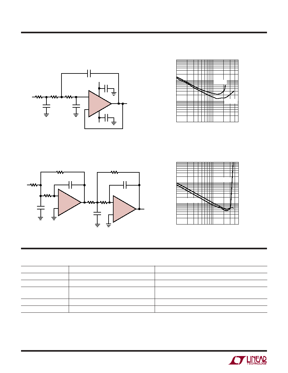
DC Accurate, 3rd Order, 100Hz, Butterworth Antialiasing Filter
Dynamic Range
DC Accurate, 18-Bit, 4th Order Antialiasing Bessel (Linear Phase),
100Hz, Lowpass Filter
Dynamic Range
TYPICAL APPLICATIO S
U
RELATED PARTS