 | ÐлекÑÑоннÑй компоненÑ: LTC1069-6 | СкаÑаÑÑ:  PDF PDF  ZIP ZIP |
Äîêóìåíòàöèÿ è îïèñàíèÿ www.docs.chipfind.ru
1
LTC1069-6
Single Supply, Very Low
Power, Elliptic Lowpass Filter
FEATURES
DESCRIPTIO
N
U
The LTC
®
1069-6 is a monolithic low power, 8th order low-
pass filter optimized for single 3V or single 5V supply
operation. The LTC1069-6 typically consumes 1mA under
single 3V supply operation and 1.2mA under 5V operation.
The cutoff frequency of the LTC1069-6 is clock tunable and it
is equal to the clock frequency divided by 50. The input signal
is sampled twice per clock cycle to lower the risk of aliasing.
The typical passband ripple is
±
0.1dB up to 0.9f
CUTOFF
.
The gain at f
CUTOFF
is 0.7dB. The transition band of the
LTC1069-6 features progressive attenuation reaching 42dB
at 1.3f
CUTOFF
and 70dB at 2.1f
CUTOFF
. The maximum
stopband attenuation is 72dB.
The LTC1069-6 can be clock tuned for cutoff frequencies
up to 20kHz (single 5V supply) and for cutoff frequencies
up to 14kHz (single 3V supply).
The low power feature of the LTC1069-6 does not penalize
the device's dynamic range. With single 5V supply and an
input range of 0.4V
RMS
to 1.4V
RMS
, the Signal-to-(Noise
+ THD) ratio is
70dB. The wideband noise of the
LTC1069-6 is 125
µ
V
RMS
.
Other filter responses with higher speed can be obtained.
Please contact LTC Marketing for details.
The LTC1069-6 is available in an 8-pin SO package.
s
8th Order Elliptic Filter in SO-8 Package
s
Single 3V Operation: Supply Current: 1mA (Typ)
f
CUTOFF
: 14kHz (Max)
S/N Ratio: 72dB
s
Single 5V Operation: Supply Current: 1.2mA (Typ)
f
CUTOFF
: 20kHz (Max)
S/N Ratio: 79dB
s
±
0.1dB Passband Ripple Up to 0.9f
CUTOFF
(Typ)
s
42dB Attenuation at 1.3f
CUTOFF
s
66dB Attenuation at 2.0f
CUTOFF
s
70dB Attenuation at 2.1f
CUTOFF
s
Wide Dynamic Range, 75dB or More (S/N + THD),
Under Single 5V Operation
s
Wideband Noise: 120
µ
V
RMS
s
Clock-to-f
CUTOFF
Ratio: 50:1
s
Internal Sample Rate: 100:1
, LTC and LT are registered trademarks of Linear Technology Corporation.
s
Handheld Instruments
s
Telecommunication Filters
s
Antialiasing Filters
s
Smoothing Filters
s
Audio
s
Multimedia
APPLICATIO
N
S
U
TYPICAL APPLICATIO
N
U
Frequency Response
FREQUENCY (kHz)
5
80
GAIN (dB)
70
50
40
30
15
10
1069-6 TA02
60
10
20
25
20
10
0
V
IN
= 500mV
RMS
Single 3V Supply 10kHz Elliptic Lowpass Filter
AGND
V
+
NC
V
IN
V
OUT
V
NC
CLK
LTC1069-6
f
CLK
= 500kHz
3V
0.47
µ
F
0.1
µ
F
1069-6 TA01
2
LTC1069-6
ABSOLUTE
M
AXI
M
U
M
RATINGS
W
W
W
U
PACKAGE/ORDER I
N
FOR
M
ATIO
N
W
U
U
LTC1069-6CS8
LTC1069-6IS8
f
CUTOFF
is the filter's cutoff frequency and is equal to f
CLK
/50. The f
CLK
signal level is TTL or CMOS (clock rise or fall time
1
µ
s)
R
L
= 10k, V
S
= 5V, T
A
= 25
°
C, unless otherwise specified. All AC gains are measured relative to the passband gain.
PARAMETER
CONDITIONS
MIN
TYP
MAX
UNITS
Passband Gain (f
IN
0.2f
CUTOFF
)
V
S
= 5V, f
CLK
= 200kHz
0.25
0.1
0.45
dB
f
TEST
= 0.25kHz, V
IN
= 1V
RMS
q
0.30
0.1
0.50
dB
V
S
= 3V, f
CLK
= 200kHz
0.25
0.1
0.45
dB
f
TEST
= 0.25kHz, V
IN
= 0.5V
RMS
q
0.30
0.1
0.50
dB
Gain at 0.50f
CUTOFF
V
S
= 5V, f
CLK
= 200kHz
0.10
0.07
0.25
dB
f
TEST
= 2.0kHz, V
IN
= 1V
RMS
q
0.15
0.07
0.30
dB
V
S
= 3V, f
CLK
= 200kHz
0.15
0.07
0.25
dB
f
TEST
= 2.0kHz, V
IN
= 0.5V
RMS
q
0.20
0.07
0.30
dB
Gain at 0.75f
CUTOFF
V
S
= 5V, f
CLK
= 200kHz
0.25
0
0.25
dB
f
TEST
= 3.0kHz, V
IN
= 1V
RMS
q
0.30
0
0.30
dB
V
S
= 3V, f
CLK
= 200kHz
0.25
0
0.25
dB
f
TEST
= 3.0kHz, V
IN
= 0.5V
RMS
q
0.30
0
0.30
dB
Gain at 0.90f
CUTOFF
V
S
= 5V, f
CLK
= 200kHz
0.25
0.1
0.45
dB
f
TEST
= 3.6kHz, V
IN
= 1V
RMS
q
0.25
0.1
0.45
dB
V
S
= 3V, f
CLK
= 200kHz
0.25
0.1
0.45
dB
f
TEST
= 3.6kHz, V
IN
= 0.5V
RMS
q
0.30
0.1
0.50
dB
Gain at 0.95f
CUTOFF
V
S
= 5V, f
CLK
= 200kHz
0.35
0.05
0.25
dB
f
TEST
= 3.8kHz, V
IN
= 1V
RMS
q
0.45
0.05
0.25
dB
V
S
= 3V, f
CLK
= 200kHz
0.45
0.05
0.25
dB
f
TEST
= 3.8kHz, V
IN
= 0.5V
RMS
q
0.55
0.05
0.35
dB
Gain at f
CUTOFF
V
S
= 5V, f
CLK
= 200kHz
1.50
0.07
0.20
dB
f
TEST
= 4.0kHz, V
IN
= 1V
RMS
q
1.65
0.07
0.25
dB
V
S
= 3V, f
CLK
= 200kHz
1.5
0.07
0
dB
f
TEST
= 4.0kHz, V
IN
= 0.5V
RMS
q
1.7
0.07
0
dB
Gain at 1.30f
CUTOFF
V
S
= 5V, f
CLK
= 200kHz
42
40
dB
f
TEST
= 5.2kHz, V
IN
= 1V
RMS
q
42
39
dB
V
S
= 3V, f
CLK
= 200kHz
41
38
dB
f
TEST
= 5.2kHz, V
IN
= 0.5V
RMS
q
41
37
dB
Consult factory for Military grade parts.
ORDER PART
NUMBER
S8 PART MARKING
10696
10696I
T
JMAX
= 125
°
C,
JA
= 110
°
C/ W
1
2
3
4
8
7
6
5
TOP VIEW
V
OUT
V
NC
CLK
AGND
V
+
NC
V
IN
S8 PACKAGE
8-LEAD PLASTIC SO
Total Supply Voltage (V
+
to V
) .............................. 12V
Operating Temperature Range
LTC1069-6C ............................................ 0
°
C to 70
°
C
LTC1069-6I ........................................ 40
°
C to 85
°
C
Storage Temperature ............................ 65
°
C to 150
°
C
Lead Temperature (Soldering, 10 sec).................. 300
°
C
ELECTRICAL CHARACTERISTICS
3
LTC1069-6
f
CUTOFF
is the filter's cutoff frequency and is equal to f
CLK
/50. The f
CLK
signal level is TTL or CMOS (clock rise or fall time
1
µ
s)
R
L
= 10k, V
S
= 5V, T
A
= 25
°
C, unless otherwise specified. All AC gains are measured relative to the passband gain.
PARAMETER
CONDITIONS
MIN
TYP
MAX
UNITS
Gain at 2.00f
CUTOFF
V
S
= 5V, f
CLK
= 200kHz
66
61
dB
f
TEST
= 8.0kHz, V
IN
= 1V
RMS
q
66
60
dB
V
S
= 3V, f
CLK
= 200kHz
66
60
dB
f
TEST
= 8.0kHz, V
IN
= 0.5V
RMS
q
66
59
dB
Gain at 0.95f
CUTOFF
V
S
= 5V, f
CLK
= 400kHz, f
TEST
= 7.6kHz, V
IN
= 1V
RMS
0.5
0.15
0.5
dB
V
S
= 3V, f
CLK
= 400kHz, f
TEST
= 7.6kHz, V
IN
= 0.5V
RMS
0.5
0
0.5
dB
Output DC Offset (Note 1)
V
S
= 5V, f
CLK
= 100kHz
50
175
mV
V
S
= 3V, f
CLK
= 100kHz
30
135
mV
Output DC Offset Tempco
V
S
= 5V, V
S
= 3V
30
µ
V/
°
C
Output Voltage Swing (Note 2)
V
S
= 5V, f
CLK
= 100kHz
3.4
4.2
V
P-P
q
3.2
4.2
V
P-P
V
S
= 3V, f
CLK
= 100kHz
1.6
2.0
V
P-P
q
1.5
2.0
V
P-P
Power Supply Current
V
S
= 5V, f
CLK
= 100kHz
1.2
1.60
mA
q
1.65
mA
V
S
= 3V, f
CLK
= 100kHz
1.0
1.40
mA
q
1.55
mA
Maximum Clock Frequency
V
S
= 5V
1.0
MHz
V
S
= 3V
0.7
MHz
Input Frequency Range
0
<(f
CLK
2f
C
)
Input Resistance
35
50
80
k
Operating Supply Voltage (Note 3)
3
10
V
FREQUENCY (kHz)
20
80
GAIN (dB)
78
74
72
70
60
66
40
60
1069-6 G03
76
64
62
68
80
100
V
S
= SINGLE 3V
f
CLK
= 500kHz
f
CUTOFF
= 10kHz
V
IN
= 0.5V
RMS
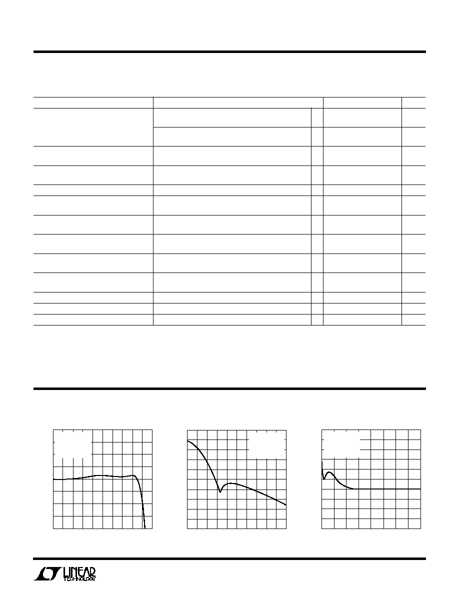
Transition Band Gain vs Frequency
FREQUENCY (kHz)
10
GAIN (dB)
30
10
10
18
1069-6 G02
50
70
40
20
0
60
80
90
12
14
16
20
V
S
= SINGLE 3V
f
CLK
= 500kHz
f
CUTOFF
= 10kHz
V
IN
= 0.5V
RMS
Stopband Gain vs Frequency
FREQUENCY (kHz)
1
GAIN (dB)
1
2
9
1069-6 G01
0
1
2
3
5
7
11
V
S
= SINGLE 3V
f
CLK
= 500kHz
f
CUTOFF
= 10kHz
V
IN
= 0.5V
RMS
Passband Gain vs Frequency
The
q
denotes specifications which apply over the full operating
temperature range.
Note 1: The input offset voltage is measured with respect to AGND (Pin 1).
The input (Pin 4) is also shorted to the AGND pin. The analog ground pin
potential is internally set to (0.437)(V
SUPPLY
).
Note 2: The input voltage can swing to either rail (V
+
or ground); the
output typically swings 50mV from ground and 0.8V from V
+
.
Note 3: The LTC1069-6 is optimized for 3V and 5V operation. Although the
device can operate with a single 10V supply or
±
5V, the total harmonic
distortion will be degraded. For single 10V or
±
5V supply operation we
recommend to use the LTC1069-1.
TYPICAL PERFOR
M
A
N
CE CHARACTERISTICS
U
W
ELECTRICAL CHARACTERISTICS
4
LTC1069-6
TYPICAL PERFOR
M
A
N
CE CHARACTERISTICS
U
W
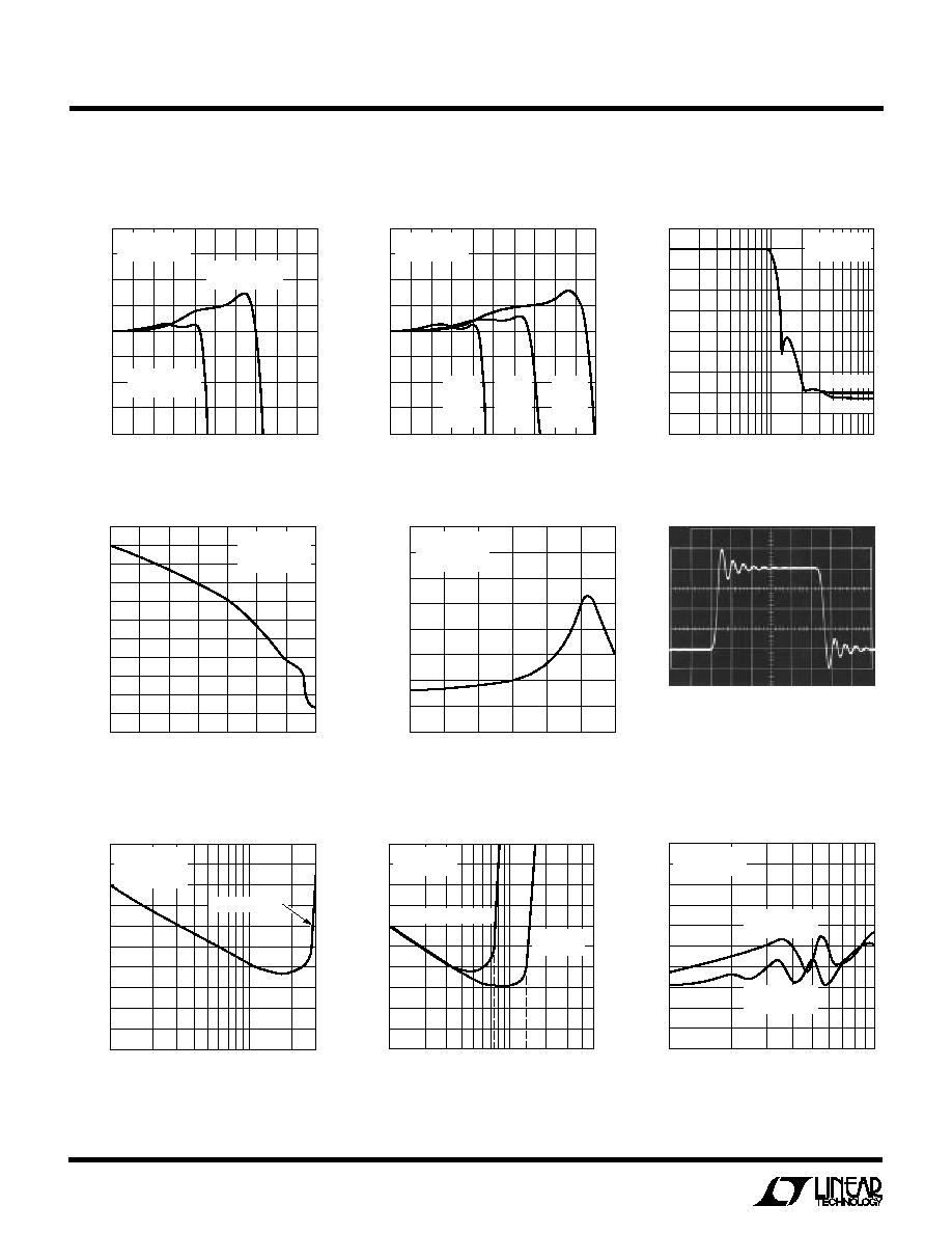
Amplitude Response
vs Supply Voltage
Passband Gain vs Clock Frequency
FREQUENCY (kHz)
1
GAIN (dB)
1
2
17 19
1069-6 G05
0
1
2
5
9
13 15
3
7
11
21
V
S
= SINGLE 5V
V
IN
= 1V
RMS
f
CLK
500kHz
f
CUTOFF
10kHz
f
CLK
750kHz
f
CUTOFF
15kHz
f
CLK
1MHz
f
CUTOFF
20kHz
FREQUENCY (kHz)
1
90
GAIN (db)
70
50
30
10
10
100
1069-6 G06
10
80
60
40
20
0
f
CLK
= 500kHz
V
IN
= 0.5V
RMS
SINGLE 5V
SINGLE 3V
Transient Response
FREQUENCY (kHz)
0
PHASE (DEG)
630
90
0
90
4
8
10
1069-6 G07
810
270
450
720
180
900
360
540
2
6
12
14
V
S
= SINGLE 5V
f
CLK
= 500kHz
f
CUTOFF
= 10kHz
Phase vs Frequency
Passband Gain vs Clock Frequency
FREQUENCY (kHz)
1
GAIN (dB)
1
2
17 19
1069-6 G04
0
1
2
5
9
13 15
3
7
11
21
V
S
= SINGLE 3V
V
IN
= 0.5V
RMS
f
CLK
= 500kHz
f
CUTOFF
= 10kHz
f
CLK
= 750kHz
f
CUTOFF
= 15kHz
1069-6 G09
V
S
= SINGLE 5V
0.1ms/DIV
f
CLK
= 1MHz
f
IN
= 1kHz
2V
P-P
SQUAREWAVE
0.5
V
/DIV
Group Delay vs Frequency
FREQUENCY (kHz)
0
GROUP DELAY (SEC)
6
10
1069-6 G08
2
4
8
4.00E-04
3.50E-04
3.00E-04
2.50E-04
2.00E-04
1.50E-04
1.00E-04
5.00E-05
0.00E+00
12
V
S
= SINGLE 5V
f
CLK
= 500kHz
f
CUTOFF
= 10kHz
THD + Noise vs Frequency
FREQUENCY (kHz)
1
5
10
1069-6 G11
90
THD + NOISE (dB)
80
70
60
50
85
75
65
55
45
40
f
CLK
= 500kHz
f
CUTOFF
= 10kHz
V
S
= SINGLE 3V
V
IN
= 0.5V
RMS
V
S
= SINGLE 5V
V
IN
= 1V
RMS
Dynamic Range THD + Noise
vs Input Voltage
INPUT VOLTAGE (V
RMS
)
0.1
0.5 0.76
1.43
90
THD + NOISE (dB)
80
70
60
50
1
5
1069-6 G10
85
75
65
55
45
40
f
CLK
= 500kHz
f
IN
= 1kHz
V
S
= SINGLE 3V
V
S
=
SINGLE 5V
INPUT/OUTPUT VOLTAGE (V
P-P
)
0.1
90
THD + NOISE (dB)
80
70
60
50
1
3
1069-6 G14
85
75
65
55
45
40
f
CLK
= 170kHz
f
CUTOFF
= 3.4kHz
f
IN
= 1kHz
V
IN
= 2.945V
P-P
Dynamic Range THD + Noise
vs Input/Output Voltage
5
LTC1069-6
TYPICAL PERFOR
M
A
N
CE CHARACTERISTICS
U
W
Output Voltage Swing
vs Temperature
AMBIENT TEMPERATURE (
°
C)
40
20
0
20
40
60
80
0
POSITIVE SWING (V)
NEGATIVE SWING (mV)
20
40
60
80
4.5
2.5
4.0
2.0
1069-6 G13
R
L
= 10k
V
S
= SINGLE 5V
V
S
= SINGLE 3V
V
S
= SINGLE 3V
V
S
= SINGLE 5V
Supply Current vs Supply Voltage
TOTAL SUPPLY VOLTAGE (V)
0
0
SUPPLY CURRENT (mA)
2
5
4
8
10
1069-6 G12
1
4
3
2
6
12
14
16
85
°
C
40
°
C
25
°
C
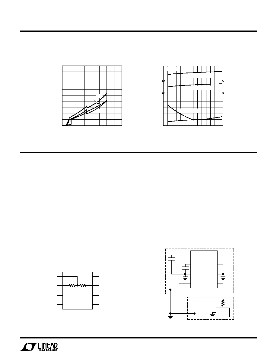
AGND (Pin 1): Analog Ground. The quality of the analog
signal ground can affect the filter performance. For either
single or dual supply operation, an analog ground plane
surrounding the package is recommended. The analog
ground plane should be connected to any digital ground at
a single point. For single supply operation, Pin 1 should be
bypassed to the analog ground plane with a 0.47
µ
F capaci-
tor or larger. An internal resistive divider biases Pin 1 to
0.4366 times the total power supply of the device (Figure
1). That is, with a single 5V supply, the potential at Pin 1
is 2.183V
±
1%. As the LTC1069-6 is optimized for single
supply operation, the internal biasing of Pin 1 allows
optimum output swing. The AGND pin should be buffered
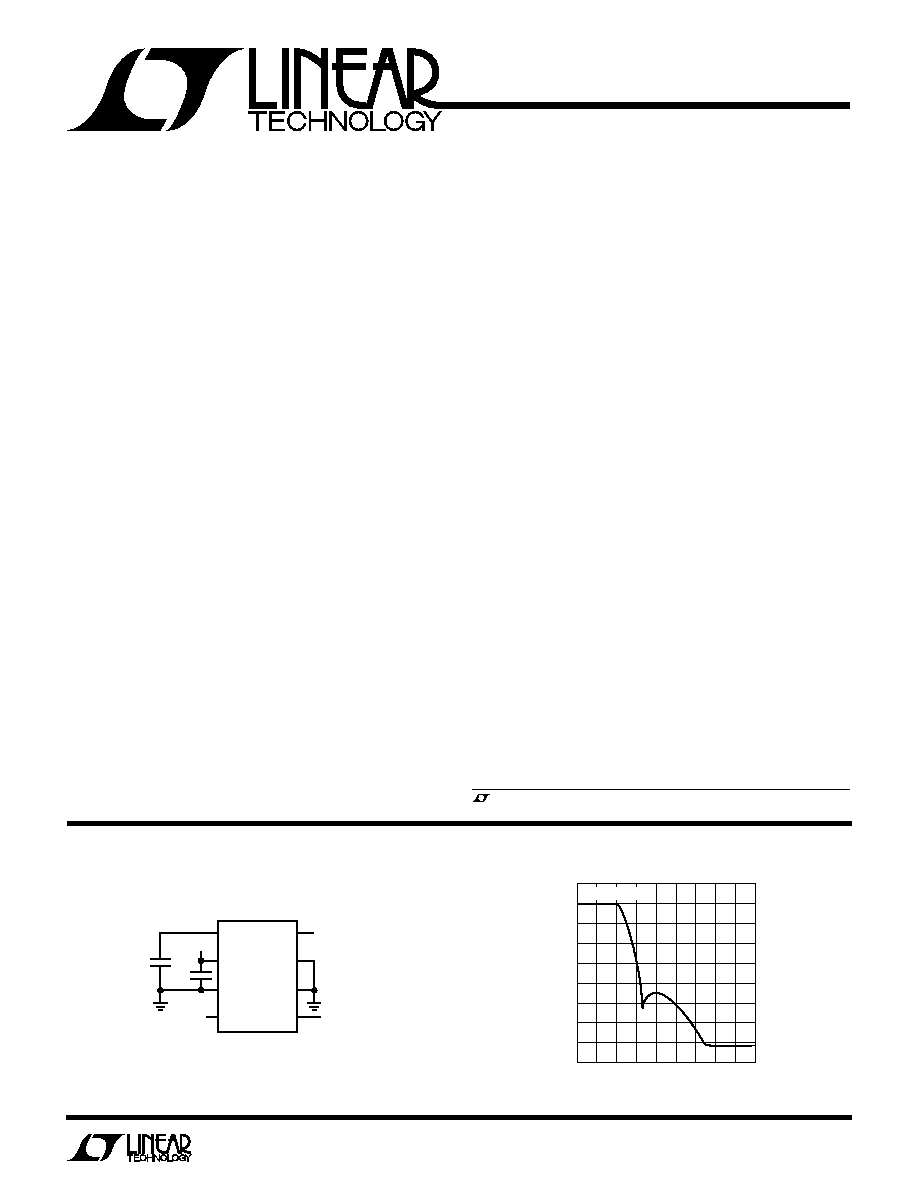
if used to bias other ICs. Figure 2 shows the connections
for single supply operation.
PI
N
FU
N
CTIO
N
S
U
U
U
Figure 1. Internal Biasing of the Analog Ground (Pin 1)
V
+
NC
V
IN
V
OUT
V
1
2
3
4
8
7
6
5
NC
CLK
LTC1069-6
1069-6 F01
AGND
11.325k 8.775k
V
+
, V
(Pins 2, 7): Power Supply Pins. The V
+
(Pin 2) and
the V
(Pin 7, if used) should be bypassed with a 0.1
µ
F
capacitor to an adequate analog ground. The filter's power
supplies should be isolated from other digital or high
voltage analog supplies. A low noise linear supply is
recommended. Switching power supplies will lower the
signal-to-noise ratio of the filter. Unlike previous mono-
lithic filters, the power supplies can be applied in any
order, that is, the positive supply can be applied before the
negative supply and vice versa. Figure 3 shows the con-
nection for dual supply operation.
AGND
V
+
V
+
NC
V
IN
V
IN
V
OUT
V
OUT
V
1
2
3
4
8
7
6
5
1k
NC
CLK
LTC1069-6
ANALOG GROUND PLANE
DIGITAL
GROUND
PLANE
0.47
µ
F
0.1
µ
F
1069-6 F02
CLOCK
SOURCE
STAR
SYSTEM
GROUND
Figure 2. Connections for Single Supply Operation