 | –≠–ª–µ–∫—Ç—Ä–æ–Ω–Ω—ã–π –∫–æ–º–ø–æ–Ω–µ–Ω—Ç: LTC1093 | –°–∫–∞—á–∞—Ç—å:  PDF PDF  ZIP ZIP |
1
LTC1091/LTC1092
LTC1093/LTC1094
1-, 2-, 6- and 8-Channel, 10-Bit
Serial I/O Data Acquisition Systems
s
Programmable Features
≠ Unipolar/Bipolar Conversions
≠ Differential/Single-Ended Multiplexer
Configurations
s
Sample-and-Holds
s
Single Supply 5V, 10V or
±
5V Operation
s
Direct 3- or 4-Wire Interface to Most MPU Serial
Ports and All MPU Parallel I/O Ports
s
Analog Inputs Common Mode to Supply Rails
s
Resolution: 10 Bits
s
Total Unadjusted Error (A Grade):
±
1LSB Over Temp
s
Fast Conversion Time: 20
µ
s
s
Low Supply Current
LTC1091: 3.5mA Max, 1.5mA Typ
LTC1092/LTC1093/LTC1094: 2.5mA Max, 1mA Typ
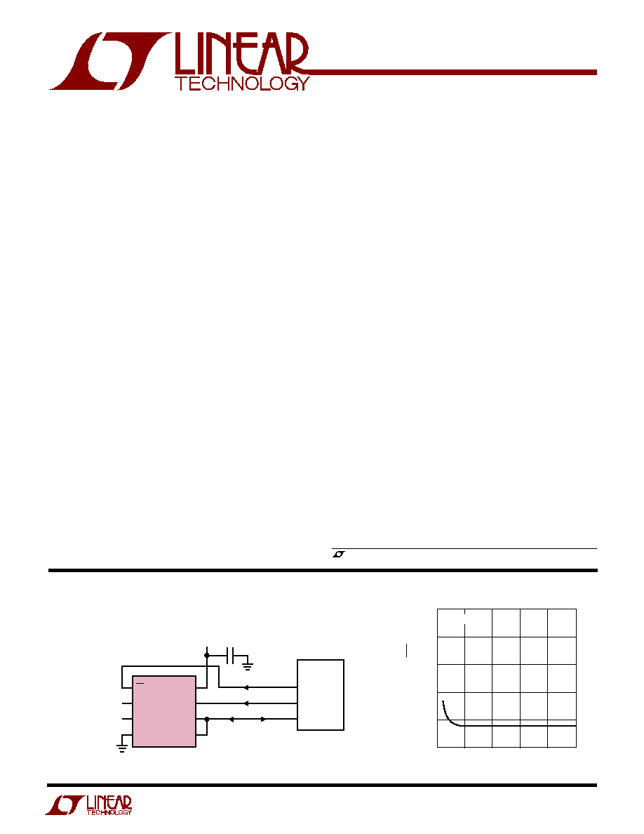
5V
ANALOG INPUT #1
0V TO 5V RANGE
ANALOG INPUT #2
0V TO 5V RANGE
CLK
D
OUT
D
IN
CS
CH0
CH1
GND
LTC1091
MPU
(e.g., 8051)
P1.4
P1.3
P1.2
1091 TA01
8
7
6
5
1
2
3
4
SERIAL DATA LINK
FOR 8051 CODE SEE
APPLICATIONS INFORMATION
SECTION
V
CC
(V
REF
)
4.7
µ
F
REFERENCE VOLTAGE (V)
0
LINEARITY ERROR (LSB = ∑ V
REF
)
1.25
1.00
0.75
0.50
0.25
0
4
1091 TA02
1
2
3
5
1
1024
V
CC
= 5V
The LTC
Æ
1091/LTC1092/LTC1093/LTC1094 10-bit data
acquisition systems are designed to provide complete
function, excellent accuracy and ease of use when digitiz-
ing analog data from a wide variety of signal sources and
transducers. Built around a 10-bit, switched capacitor,
successive approximation A/D core, these devices include
software configurable analog multiplexers and bipolar and
unipolar conversion modes as well as on-chip sample-
and-holds. On-chip serial ports allow efficient data trans-
fer to a wide range of microprocessors and microcontrol-
lers. These circuits can provide a complete data acquisi-
tion system in ratiometric applications or can be used with
an external reference in others.
The high impedance analog inputs and the ability to
operate with reduced spans (below 1V full scale) allow
direct connection to sensors and transducers in many
applications, eliminating the need for gain stages.
An efficient serial port communicates without external
hardware to most MPU serial ports and all MPU parallel
I/O ports allowing eight channels of data to be transmitted
over as few as three wires. This, coupled with low power
consumption, makes remote location possible and facili-
tates transmitting data through isolation barriers.
Temperature drift of offset, linearity and full-scale error
are all extremely low (1ppm/
∞
C typically) allowing all
grades to be specified with offset and linearity errors of
±
0.5LSB maximum over temperature. In addition, the A
grade devices are specified with full-scale error and total
unadjusted error (including the effects of offset, linearity
and full-scale errors) of
±
1LSB maximum over tempera-
ture. The lower grade has a full-scale specification of
±
2LSB for applications where full scale is adjustable or
less critical.
, LTC and LT are registered trademarks of Linear Technology Corporation.
FEATURES
DESCRIPTIO
U
TYPICAL APPLICATIO
N
U
2
LTC1091/LTC1092
LTC1093/LTC1094
W
U
U
PACKAGE/ORDER I FOR ATIO
ORDER PART
NUMBER
ORDER PART
NUMBER
LTC1091ACN8
LTC1091CN8
1
2
3
4
8
7
6
5
TOP VIEW
CS
+IN
≠IN
GND
V
CC
CLK
D
OUT
V
REF
N8 PACKAGE
8-LEAD PDIP
T
JMAX
= 110
∞
C,
JA
= 150
∞
C/W (N)
LTC1092ACN8
LTC1092CN8
1
2
3
4
8
7
6
5
TOP VIEW
CS
CH0
CH1
GND
V
CC
(V
REF
)
CLK
D
OUT
D
IN
N8 PACKAGE
8-LEAD PDIP
T
JMAX
= 110
∞
C,
JA
= 150
∞
C/W (N)
LTC1093ACN
LTC1093CN
LTC1093CSW
1
2
3
4
5
6
7
8
9
10
TOP VIEW
N PACKAGE
20-LEAD PDIP
20
19
18
17
16
15
14
13
12
11
CH0
CH1
CH2
CH3
CH4
CH5
CH6
CH7
COM
DGND
DV
CC
AV
CC
CLK
CS
D
OUT
D
IN
REF
+
REF
≠
AGND
V
≠
LTC1094ACN
LTC1094CN
REDUCED SPAN
CONVERSION MODES
CAPABILITY
±
5V
PART NUMBER
#CHANNELS
UNIPOLAR
BIPOLAR
(SEPARATE V
REF
)
CAPABILITY
LTC1091
2
q
Pin-for-Pin 10-Bit Upgrade of ADC0832
LTC1092
1
q
q
Pin-for-Pin 10-Bit Upgrade of ADC0831
LTC1093
6
q
q
q
q
LTC1094
8
q
q
q
q
PRODUCT GUIDE
T
JMAX
= 110
∞
C,
JA
= 150
∞
C/W (N)
T
JMAX
= 110
∞
C,
JA
= 130
∞
C/W (SW)
1
2
3
4
5
6
7
8
TOP VIEW
SW PACKAGE
16-LEAD PLASTIC SO WIDE
N PACKAGE
16-LEAD PDIP
16
15
14
13
12
11
10
9
CH0
CH1
CH2
CH3
CH4
CH5
COM
DGND
V
CC
CLK
CS
D
OUT
D
IN
V
REF
AGND
V
≠
T
JMAX
= 110
∞
C,
JA
= 150
∞
C/W (N)
Supply Voltage (V
CC
) to GND or V
≠
........................ 12V
Negative Supply Voltage (V
≠
) .................... ≠ 6V to GND
Voltage
Analog Reference and LTC1091/2 CS
Inputs ................................. (V
≠
) ≠ 0.3V to (V
CC
+ 0.3V)
Digital Inputs (except LTC1091/2 CS) .. ≠ 0.3V to 12V
Digital Outputs ........................ ≠ 0.3V to (V
CC
+ 0.3V)
A
U
G
W
A
W
U
W
A
R
BSOLUTE
XI
TI
S
Power Dissipation ............................................. 500mW
Operating Temperature Range
LTC1091/2/3/4AC, LTC1091/2/3/4C..... ≠ 40
∞
C to 85
∞
C
Storage Temperature Range ................ ≠ 65
∞
C to 150
∞
C
Lead Temperature (Soldering, 10 sec.)................ 300
∞
C
(Notes 1, 2)
Consult factory for Industrial and Military grade parts.

3
LTC1091/LTC1092
LTC1093/LTC1094
CO
N
VERTER A
N
D
M
ULTIPLEXER CHARACTERISTICS
U
W
U
LTC1091A/LTC1092A
LTC1091/LTC1092
LTC1093A/LTC1094A
LTC1093/LTC1094
PARAMETER
CONDITIONS
MIN
TYP
MAX
MIN
TYP
MAX
UNITS
Offset Error
(Note 4)
q
±
0.5
±
0.5
LSB
Linearity Error
(Notes 4, 5)
q
±
0.5
±
0.5
LSB
Full-Scale Error
(Note 4)
q
±
1.0
±
2.0
LSB
Total Unadjusted Error
V
REF
= 5.000V (Notes 4, 6)
q
±
1.0
LSB
Reference Input Resistance
LTC1092/LTC1093/LTC1094
q
5
10
5
10
k
V
REF
= 5V
Analog and REF Input Range
(Note 7)
(V
≠
) ≠ 0.05V to V
CC
+ 0.05V
V
On-Channel Leakage Current
On-Channel = 5V
q
1
1
µ
A
(Note 8)
Off-Channel = 0V
On-Channel = 0V
q
≠ 1
≠ 1
µ
A
Off-Channel = 5V
Off-Channel Leakage Current
On-Channel = 5V
q
≠ 1
≠ 1
µ
A
(Note 8)
Off-Channel = 0V
On-Channel = 0V
q
1
1
µ
A
Off-Channel = 5V
The
q
denotes specifications which apply over the full operating temperature range, otherwise specifications are T
A
= 25
∞
C. (Note 3)
RECO
E
DED OPERATI
G CO DITIO
S
U
U
U
U
W
W
LTC1091A/LTC1092A/LTC1093A/LTC1094A
LTC1091/LTC1092/LTC1093/LTC1094
SYMBOL
PARAMETER
CONDITIONS
MIN
MAX
UNITS
V
CC
Supply Voltage
4.5
10
V
V
≠
Negative Supply Voltage
LTC1093/LTC1094, V
CC
= 5V
≠ 5.5
0
V
f
CLK
Clock Frequency
V
CC
= 5V
0.01
0.5
MHz
t
CYC
Total Cycle Time
LTC1091
15 CLK Cycles
+ 2
µ
s
LTC1092
12 CLK Cycles
+ 2
µ
s
LTC1093/LTC1094
18 CLK Cycles
+ 2
µ
s
t
hDI
Hold Time, D
IN
Alter SCLK
V
CC
= 5V
150
ns
t
suCS
Setup Time CS
Before CLK
V
CC
= 5V
1
µ
s
t
suDI
Setup Time D
IN
Stable Before CLK
V
CC
= 5V
400
ns
t
WHCLK
CLK High Time
V
CC
= 5V
0.8
µ
s
t
WLCLK
CLK Low Time
V
CC
= 5V
1
µ
s
t
WHCS
CS High Time Between Data Transfer Cycles V
CC
= 5V
2
µ
s
t
WLCS
CS Low Time During Data Transfer
LTC1091
15
CLK Cycles
LTC1092
12
CLK Cycles
LTC1093/LTC1094
18
CLK Cycles
4
LTC1091/LTC1092
LTC1093/LTC1094
AC CHARACTERISTICS
The
q
denotes specifications which apply over the full operating temperature range, otherwise specifications are T
A
= 25
∞
C. (Note 3)
LTC1091A/LTC1092A/LTC1093A/LTC1094A
LTC1091/LTC1092/LTC1093/LTC1094
SYMBOL
PARAMETER
CONDITIONS
MIN
TYP
MAX
UNITS
t
SMPL
Analog Input Sample Time
See Operating Sequence
1.5
CLK Cycles
t
CONV
Conversion Time
See Operating Sequence
10
CLK Cycles
t
dDO
Delay Time, CLK
to D
OUT
Data Valid
See Test Circuits
q
400
850
ns
t
dis
Delay Time, CS
to D
OUT
Hi-Z
See Test Circuits
q
180
450
ns
t
en
Delay Time, CLK
to D
OUT
Enabled
See Test Circuits
q
160
450
ns
t
hDO
Time Output Data Remains Valid After SCLK
150
ns
t
f
D
OUT
Fall Time
See Test Circuits
q
90
300
ns
t
r
D
OUT
Rise Time
See Test Circuits
q
60
300
ns
C
IN
Input Capacitance
Analog Inputs On-Channel
65
pF
Analog Inputs Off-Channel
5
pF
Digital Inputs
5
pF
The
q
denotes specifications which apply over the full operating temperature range, otherwise specifications are T
A
= 25
∞
C. (Note 3)
ELECTRICAL C
C
HARA TER STICS
DIGITAL A D
U
I
DC
LTC1091A/LTC1092A/LTC1093A/LTC1094A
LTC1091/LTC1092/LTC1093/LTC1094
SYMBOL PARAMETER
CONDITIONS
MIN
TYP
MAX
UNITS
V
IH
High Level Input Voltage
V
CC
= 5.25V
q
2.0
V
V
IL
Low Level Input Voltage
V
CC
= 4.75V
q
0.8
V
I
IH
High Level Input Current
V
IN
= V
CC
q
2.5
µ
A
I
IL
Low Level Input Current
V
IN
= 0V
q
≠2.5
µ
A
V
OH
High Level Output Voltage
V
CC
= 4.75V, I
OUT
= 10
µ
A
4.7
V
V
CC
= 4.75V, I
OUT
= 360
µ
A
q
2.4
4.0
V
V
OL
Low Level Output Voltage
V
CC
= 4.75V, I
OUT
= 1.6mA
q
0.4
V
I
OZ
Hi-Z Output Leakage
V
OUT
= V
CC
, CS High
q
3
µ
A
V
OUT
= 0V, CS High
q
≠3
µ
A
I
SOURCE
Output Source Current
V
OUT
= 0V
≠10
mA
I
SINK
Output Sink Current
V
OUT
= V
CC
10
mA
I
CC
Positive Supply Current
LTC1091, CS High
q
1.5
3.5
mA
LTC1092/LTC1093/LTC1094, CS High, REF
+
Open
q
1.0
2.5
mA
I
REF
Reference Current
LTC1092/LTC1093/LTC1094, V
REF
= 5V
q
0.5
1.0
mA
I
≠
Negative Supply Current
LTC1093/LTC1094, CS High, V
≠
= ≠ 5V
q
1
50
µ
A
Note 1: Absolute Maximum Ratings are those values beyond which the life
of a device may be impaired.
Note 2: All voltage values are with respect to ground with DGND, AGND,
GND and REF
≠
wired together (unless otherwise noted). REF
≠
is internally
connected to the AGND pin on the LTC1093. DGND, AGND, REF
≠
and V
≠
are internally connected to the GND pin on the LTC1091/LTC1092.
Note 3: V
CC
= 5V, V
REF
+
= 5V, V
REF
≠
= 0V, V
≠
= 0V for unipolar mode and
≠ 5V for bipolar mode, CLK = 0.5MHz unless otherwise specified.
Note 4: These specs apply for both unipolar (LTC1091/LTC1092/LTC1093/
LTC1094) and bipolar (LTC1093/LTC1094 only) modes. In bipolar mode,
one LSB is equal to the bipolar input span (2V
REF
) divided by 1024. For
example, when V
REF
= 5V, 1LSB (bipolar) = 2(5V)/1024 = 9.77mV.
Note 5: Linearity error is specified between the actual end points of the
A/D transfer curve.
Note 6: Total unadjusted error includes offset, full scale, linearity,
multiplexer and hold step errors.
Note 7: Two on-chip diodes are tied to each reference and analog input
which will conduct for reference or analog input voltages one diode drop
below V
≠
or one diode drop above V
CC
. Be careful during testing at low
V
CC
levels (4.5V), as high level reference or analog inputs (5V) can cause
this input diode to conduct, especially at elevated temperatures, and cause
errors for inputs near full scale. This spec allows 50mV forward bias of
either diode. This means that as long as the reference or analog input does
not exceed the supply voltage by more than 50mV, the output code will be
correct. To achieve an absolute 0V to 5V input voltage range will therefore
require a minimum supply voltage of 4.950V over initial tolerance,
temperature variations and loading.
Note 8: Channel leakage current is measured after the channel selection.
5
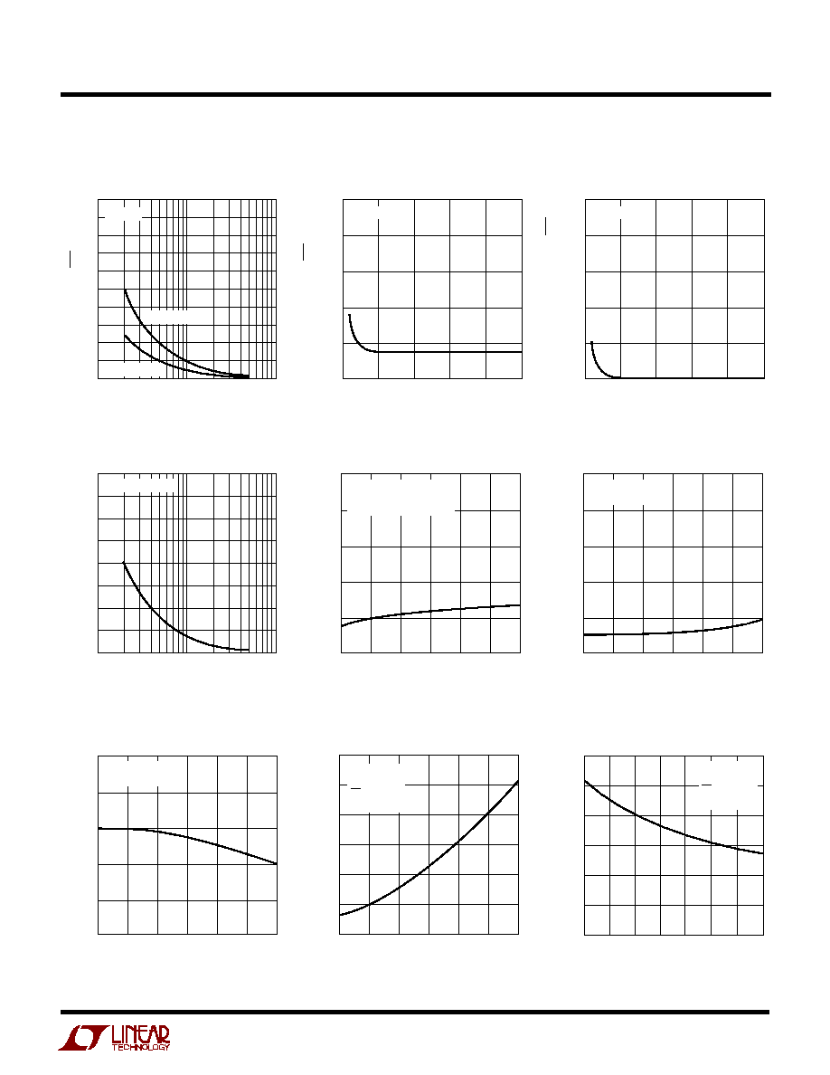
LTC1091/LTC1092
LTC1093/LTC1094
Change in Full-Scale Error vs
Temperature
AMBIENT TEMPERATURE (
∞
C)
≠50
MAGNITUDE OF OFFSET CHANGE (LSB)
0.6
0.5
0.4
0.3
0.2
0.1
0
50
1091/2/3/4 G01
≠25
0
25
75
125
100
V
CC
(V
REF
) = 5V
f
CLK
= 500kHz
Change in Offset Error vs
Temperature
AMBIENT TEMPERATURE (
∞
C)
≠50
MAGNITUDE OF FULL-SCALE CHANGE (LSB)
0.6
0.5
0.4
0.3
0.2
0.1
0
50
1091/2/3/4 G03
≠25
0
25
75
125
100
V
CC
(V
REF
) = 5V
f
CLK
= 500kHz
AMBIENT TEMPERATURE (
∞
C)
≠50
MAGNITUDE OF LINEARITY CHANGE (LSB)
0.6
0.5
0.4
0.3
0.2
0.1
0
50
1091/2/3/4 G02
≠25
0
25
75
125
100
V
CC
(V
REF
) = 5V
f
CLK
= 500kHz
Change in Linearity Error vs
Temperature
AMBIENT TEMPERATURE (
∞
C)
≠50
D
OUT
DELAY TIME FROM SCLK
(ns)
600
500
400
300
200
100
0
50
1091/2/3/4 G05
≠25
0
25
75
125
100
V
CC
= 5V
MSB-FIRST DATA
LSB-FIRST DATA
Digital Input Logic Threshold vs
Supply Voltage
D
OUT
Delay Time vs Temperature
D
OUT
Delay Time vs
Supply Voltage
SUPPLY VOLTAGE (V)
4
5
6
7
8
1091/2/3/4 G06
9
10
T
A
= 25
∞
C
D
OUT
DELAY TIME FROM SCLK
(ns)
600
500
400
300
200
100
0
MSB-FIRST DATA
LSB-FIRST DATA
SUPPLY VOLTAGE (V)
4
LOGIC THRESHOLD (V)
4
3
2
1
0
5
6
7
8
1091/2/3/4 G04
9
10
T
A
= 25
∞
C
Maximum Clock Rate vs
Temperature
AMBIENT TEMPERATURE (
∞
C)
≠50
MAXIMUM CLK FREQUENCY* (MHz)
3.0
2.5
2.0
1.5
1.0
0.5
0
50
1091/2/3/4 G07
≠25
0
25
75
125
100
V
CC
= 5V
Maximum Clock Rate vs
Supply Voltage
AMBIENT TEMPERATURE (
∞
C)
≠50
MINIMUM CLK FREQUENCY** (MHz)
0.3
0.25
0.20
0.15
0.10
0.05
0
50
1091/2/3/4 G09
≠25
0
25
75
125
100
V
CC
= 5V
Minimum Clock Rate vs
Temperature
SUPPLY VOLTAGE (V)
4
5
6
7
8
1091/2/3/4 G08
9
10
T
A
= 25
∞
C
MAXIMUM CLK FREQUENCY* (MHz)
3.0
2.5
2.0
1.5
1.0
0.5
0
*MAXIMUM CLK FREQUENCY REPRESENTS THE HIGHEST FREQUENCY AT WHICH CLK CAN
BE OPERATED (WITH 50% DUTY CYCLE) WHILE STILL PROVIDING 100ns SETUP TIME FOR
THE DEVICE RECEIVING THE D
OUT
DATA.
**AS THE CLK FREQUENCY IS DECREASED FROM 500kHz, MINIMUM CLK FREQUENCY
(
ERROR
0.1LSB) REPRESENTS THE FREQUENCY AT WHICH A 0.1LSB SHIFT IN ANY
CODE TRANSITION FROM ITS 500kHz VALUE IS FIRST DETECTED.
C
C
HARA TERISTICS
U
W
A
TYPICAL PERFOR
CE

6
LTC1091/LTC1092
LTC1093/LTC1094
C
C
HARA TERISTICS
U
W
A
TYPICAL PERFOR
CE
LTC1091/LTC1092/LTC1093/LTC1094
Maximum Clock Rate vs
Source Resistance
LTC1091/LTC1092/LTC1093/LTC1094
Maximum Filter Resistor vs
Cycle Time
LTC1091/LTC1092/LTC1093/LTC1094
Sample-and-Hold Acquisition Time
vs Source Resistance
R
SOURCE
(
)
10
MAXIMUM CLK FREQUENCY
(MHz)
1.25
1.00
0.75
0.50
0.25
0
100
1k
10k
1091/2/3/4 G10
V
CC
= 5V
T
A
= 25
∞
C
"+" OR "≠"
INPUT
V
IN
R
SOURCE
CYCLE TIME (
µ
s)
100
MAXIMUM R
FILTER
(
)
1k
10k
100k
10
1000
10000
1091/2/3/4 G11
10
100
+
≠
V
IN
C
FILTER
1
µ
F
R
FILTER
R
SOURCE
+ (
)
100
1k
10k
1091/2/3/4 G12
0.1
S & H ACQUISITION TIME TO 0.1% (
µ
s)
1
10
+
≠
V
IN
R
SOURCE
+
V
CC
= 5V
T
A
= 25
∞
C
0V TO 5V INPUT STEP
LTC1091 Change in Full-Scale
Error vs Supply Voltage
AMBIENT TEMPERATURE (
∞
C)
≠50
INPUT CHANNEL LEAKAGE CURRENT (nA)
100
80
60
40
20
0
50
1091/2/3/4 G13
≠25
0
25
75
125
100
ON-CHANNEL OR
OFF-CHANNEL
SUPPLY VOLTAGE (V)
4
OFFSET ERROR [LSB = ∑ V
CC
(
V
REF
)]
1.25
1.00
0.75
0.5
0.25
0
5
6
7
8
1091/2/3/4 G14
9
10
f
CLK
= 500kHz
T
A
= 25
∞
C
V
OS
= 0.85mV AT V
CC
(V
REF
) = 5V
1
1024
SUPPLY VOLTAGE (V)
4
LINEARITY ERROR [LSB = ∑ V
CC
(
V
REF
)]
1.25
1.00
0.75
0.5
0.25
0
5
6
7
8
1091/2/3/4 G15
9
10
f
CLK
= 500kHz
T
A
= 25
∞
C
1
1024
LTC1091/LTC1092 Input Channel
Leakage Current vs Temperature
LTC1091 Offset Error vs
Supply Voltage
LTC1091 Linearity Error vs
Supply Voltage
SUPPLY VOLTAGE (V)
4
CHANGE IN FULL-SCALE ERROR
[LSB = ∑ V
CC
(
V
REF
)]
0.50
0.25
0
≠0.25
≠0.50
≠0.75
5
6
7
8
1091/2/3/4 G16
9
10
f
CLK
= 500kHz
T
A
= 25
∞
C
1
1024
AMBIENT TEMPERATURE (
∞
C)
≠50
SUPPLY CURRENT (mA)
1.8
1.6
1.4
1.2
1.0
0.8
0.6
50
1091/2/3/4 G18
≠25
0
25
75
125
100
f
CLK
= 500kHz
V
CC
(V
REF
) = 5V
CS = 5V
LTC1091 Supply Current vs
Temperature
AS THE CLK FREQUENCY AND SOURCE RESISTANCE ARE INCREASED, MAXIMUM CLK
FREQUENCY (
ERROR
0.1LSB) REPRESENTS THE FREQUENCY AT WHICH A 0.1LSB
SHIFT IN ANY CODE TRANSITION FROM ITS 500kHz, 0
VALUE IS FIRST DETECTED.
MAXIMUM R
FILTER
REPRESENTS THE FILTER RESISTOR VALUE AT WHICH A 0.1LSB
CHANGE IN FULL-SCALE ERROR FROM ITS VALUE AT R
FILTER
= 0 IS FIRST DETECTED.
SUPPLY VOLTAGE (V)
SUPPLY CURRENT (mA)
7
6
5
4
3
2
1
0
1092/2/3/4 G17
4
5
6
7
8
9
10
f
CLK
= 500kHz
CS = V
CC
(V
REF
)
T
A
= 25
∞
C
LTC1091 Supply Current vs
Supply Voltage
7
LTC1091/LTC1092
LTC1093/LTC1094
C
C
HARA TERISTICS
U
W
A
TYPICAL PERFOR
CE
LTC1092/LTC1093/LTC1094
Unadjusted Offset Error vs
Reference Voltage
LTC1092/LTC1093/LTC1094
Linearity Error vs
Reference Voltage
REFERENCE VOLTAGE (V)
0
LINEARITY ERROR (LSB = ∑ V
REF
)
1.25
1.00
0.75
0.50
0.25
0
4
1092/2/3/4 G20
1
2
3
5
1
1024
V
CC
= 5V
REFERENCE VOLTAGE (V)
0
CHANGE IN FULL-SCALE ERROR (LSB = ∑ V
REF
)
1.25
1.00
0.75
0.50
0.25
0
4
1092/2/3/4 G21
1
2
3
5
1
1024
V
CC
= 5V
REFERENCE VOLTAGE (V)
0.1
0.2
1
5
10
1091/2/3/4 G19
10
9
8
7
6
5
4
3
2
1
0
V
CC
= 5V
V
OS
= 1mV
V
OS
= 0.5mV
OFFSET ERROR (LSB = ∑ V
REF
)
1
1024
LTC1092/LTC1093/LTC1094
Change in Full-Scale Error vs
Reference Voltage
SUPPLY VOLTAGE (V)
4
OFFSET ERROR (LSB)
1.25
1.00
0.75
0.50
0.25
0
5
6
7
8
1091/2/3/4 G23
9
10
V
REF
= 4V
f
CLK
= 500kHz
V
OS
= 1.25mV AT V
CC
= 5V
REFERENCE VOLTAGE (V)
0.1
0.2
1
5
10
1091/2/3/4 G22
2.00
1.75
1.50
1.25
1.00
0.75
0.50
0.25
0
NOISE = 200
µ
V
P-P
PEAK-TO-PEAK NOISE ERROR (LSB)
SUPPLY VOLTAGE (V)
4
LINEARITY ERROR (LSB)
1.25
1.00
0.75
0.50
0.25
0
5
6
7
8
1091/2/3/4 G24
9
10
V
REF
= 4V
f
CLK
= 500kHz
LTC1092/LTC1093/LTC1094
Linearity Error vs Supply Voltage
LTC1092/LTC1093/LTC1094
Offset Error vs Supply Voltage
LTC1092/LTC1093/LTC1094
Noise Error vs Reference Voltage
LTC1092/LTC1093/LTC1094
Change in Full-Scale Error vs
Supply Voltage
SUPPLY VOLTAGE (V)
4
CHANGE IN FULL-SCALE ERROR (LSB)
0.50
0.25
0
≠ 0.25
≠0.50
≠0.75
5
6
7
8
1091/2/3/4 G25
9
10
V
REF
= 4V
f
CLK
= 500kHz
SUPPLY VOLTAGE (V)
4
5
6
7
8
1091/2/3/4 G26
9
10
SUPPLY CURRENT (mA)
6
5
4
3
2
1
0
V
REF
OPEN
f
CLK
= 500kHz
CS = V
CC
T
A
= 25
∞
C
AMBIENT TEMPERATURE (
∞
C)
≠50
SUPPLY CURRENT (mA)
1.4
1.2
1.0
0.8
0.6
0.4
0.2
50
1091/2/3/4 G27
≠25
0
25
75
125
100
V
REF
OPEN
f
CLK
= 500kHz
CS = 5V
V
CC
= 5V
LTC1092/LTC1093/LTC1094
Supply Current vs Supply Voltage
LTC1092/LTC1093/LTC1094
Supply Current vs Temperature

8
LTC1091/LTC1092
LTC1093/LTC1094
LTC1092/LTC1093/LTC1094
Reference Current vs Temperature
AMBIENT TEMPERATURE (
∞
C)
≠50
REFERENCE CURRENT (mA)
0.6
0.5
0.4
0.3
0.2
0.1
0
50
1091/2/3/4 G28
≠25
0
25
75
125
100
V
REF
= 5V
AMBIENT TEMPERATURE (
∞
C)
≠50
0
INPUT CHANNEL LEAKAGE CURRENT (nA)
100
300
400
500
1000
700
0
25
50
125
1091/2/3/4 G29
200
800
900
600
≠25
75
100
ON-CHANNEL
OFF-CHANNEL
GUARANTEED
LTC1093/LTC1094 Input Channel
Leakage Current vs Temperature
PI FU CTIO S
U
U
U
LTC1091/LTC1092
CS (Pin 1): Chip Select Input. A logic low on this input
enables the LTC1091/LTC1092.
CH0, CH1/+ IN, ≠ IN (Pins 2, 3): Analog Inputs. These
inputs must be free of noise with respect to GND.
GND (Pin 4): Analog Ground. GND should be tied directly
to an analog ground plane.
D
IN
(Pin 5)(LTC1091): Digital Data Input. The multiplexer
address is shifted into this input.
V
REF
(Pin 5)(LTC1092): Reference Input. The reference
input defines the span of the A/D converter and must be
kept free of noise with respect to AGND.
D
OUT
(Pin 6): Digital Data Output. The A/D conversion
result is shifted out of this output.
CLK (Pin 7): Shift Clock. This clock synchronizes the serial
data transfer.
V
CC
(V
REF
)(Pin 8)(LTC1091): Positive Supply and Refer-
ence Voltage. This pin provides power and defines the
span of the A/D converter. It must be kept free of noise and
ripple by bypassing directly to the analog ground plane.
V
CC
(Pin 8 )(LTC1092): Positive Supply Voltage. This pin
provides power to the A/D converter. It must be kept free
of noise and ripple by bypassing directly to the analog
ground plane.
LTC1093/LTC1094
CH0 to CH5/CH0 to CH7 (Pins 1 to 6/Pins 1 to 8): Analog
Inputs. The analog inputs must be free of noise with
respect to AGND.
COM (Pin 7/Pin 9): Common. The common pin defines the
zero reference point for all single-ended inputs. It must be
free of noise and is usually tied to the analog ground plane.
DGND (Pin 8/Pin 10): Digital Ground. This is the ground
for the internal logic. Tie to the ground plane.
V
≠
(Pin 9/Pin 11): Negative Supply. Tie V
≠
to most
negative potential in the circuit. (Ground in single supply
applications.)
AGND (Pin 10/Pin 12): Analog Ground. AGND should be
tied directly to the analog ground plane.
C
C
HARA TERISTICS
U
W
A
TYPICAL PERFOR
CE
9
LTC1091/LTC1092
LTC1093/LTC1094
INPUT
SHIFT
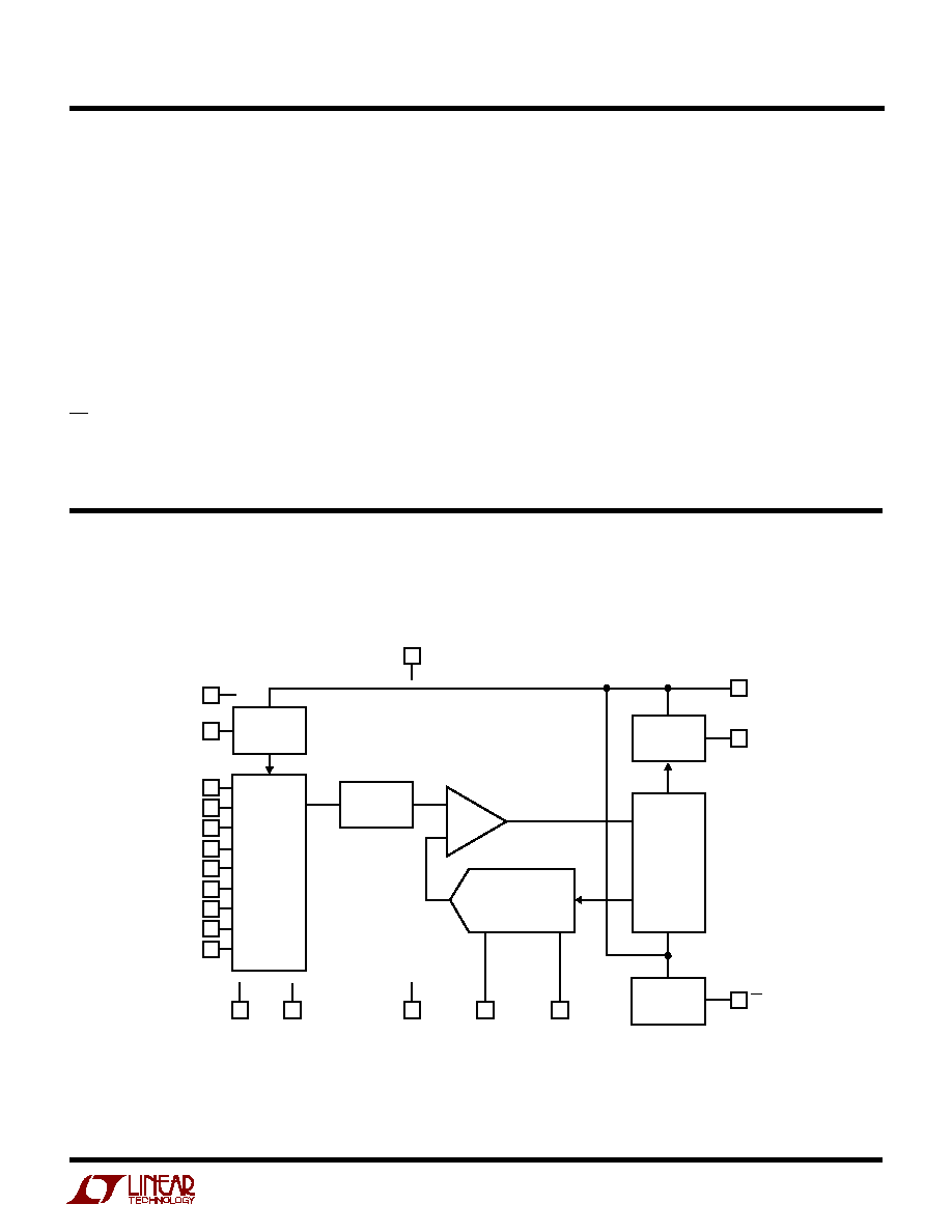
REGISTER
SAMPLE-
AND-HOLD
10-BIT
CAPACITIVE
DAC
AV
CC
ANALOG
INPUT MUX
CH0
CH1
CH2
CH3
CH4
CH5
CH6
CH7
COM
D
OUT
CLK
CONTROL
AND
TIMING
CS
1091/2/3/4 BD
REF
+
DGND
AGND
V
≠
REF
≠
COMP
OUTPUT
SHIFT
REGISTER
D
IN
10-BIT
SAR
1
2
3
4
5
6
7
8
9
10
11
12
13
14
DV
CC
19
17
16
18
15
20
(Pin numbers refer to LTC1094)
BLOCK DIAGRA
W
V
REF
(Pin 11)(LTC1093): Reference Input. The reference
input must be kept free of noise with respect to AGND.
REF
+
, REF
≠
(Pins 13, 14 )(LTC1094): Reference Input.
The reference input must be kept free of noise with respect
to AGND.
D
IN
(Pin 12/Pin 15): Data Input. The A/D configuration
word is shifted into this input.
D
OUT
(Pin 13/Pin 16): Digital Data Output. The A/D con-
version result is shifted out of this output.
CS (Pin 14/Pin 17): Chip Select Input. A logic low on this
input enables the LTC1093/LTC1094.
PI FU CTIO S
U
U
U
CLK (Pin 15/Pin 18): Shift Clock. This clock synchronizes
the serial data transfer.
V
CC
(Pin 16)(LTC1093): Positive Supply. This supply
must be kept free of noise and ripple by bypassing directly
to the analog ground plane.
AV
CC
, DV
CC
(Pins 19, 20)(LTC1094): Positive Supply.
This supply must be kept free of noise and ripple by
bypassing directly to the analog ground plane. AV
CC
and
DV
CC
should be tied together on the LTC1094.

10
LTC1091/LTC1092
LTC1093/LTC1094
On- and Off-Channel Leakage Current
Load Circuit for t
dDO
, t
r
, t
f
5V
I
OFF
I
ON
POLARITY
OFF-
CHANNELS
ON-CHANNEL
1091/2/3/4 TC01
A
A
D
OUT
1.4V
3k
100pF
TEST POINT
1091/2/3/4 TC02
CLK
D
OUT
0.8V
t
dDO
0.4V
2.4V
1091/2/3/4 TC03
Voltage Waveforms for D
OUT
Delay Time, t
dDO
D
OUT
0.4V
2.4V
t
r
t
f
1091/2/3/4 TC04
Voltage Waveforms for t
dis
D
OUT
WAVEFORM 1
(SEE NOTE 1)
2.0V
t
dis
90%
10%
D
OUT
WAVEFORM 2
(SEE NOTE 2)
CS
NOTE 1: WAVEFORM 1 IS FOR AN OUTPUT WITH INTERNAL CONDITIONS SUCH THAT
THE OUTPUT IS HIGH UNLESS DISABLED BY THE OUTPUT CONTROL
NOTE 2: WAVEFORM 2 IS FOR AN OUTPUT WITH INTERNAL CONDITIONS SUCH THAT
THE OUTPUT IS LOW UNLESS DISABLED BY THE OUTPUT CONTROL
1091/2/3/4 TC06
Voltage Waveforms for D
OUT
Rise and Fall Times, t
r
, t
f
Voltage Waveforms for t
en
1
2
3
4
LTC1091
D
IN
CLK
D
OUT
START
t
en
B9
0.4V
1091/2/3/4 TC07
CS
D
OUT
3k
100pF
TEST POINT
5V t
dis
WAVEFORM 2, t
en
t
dis
WAVEFORM 1
1091/2/3/4 TC05
Load Circuit for t
dis
, t
en
TEST CIRCUITS

11
LTC1091/LTC1092
LTC1093/LTC1094
TEST CIRCUITS
Voltage Waveforms for t
en
1
LTC1092
CLK
D
OUT
t
en
B9
0.4V
1091/2/3/4 TC08
CS
CS
B9
D
OUT
t
en
0.4V
CLK
LTC1093/LTC1094
1091/2/3/4 TC09
START
7
4
5
6
3
2
1
D
IN
U
S
A
O
PPLICATI
W
U
U
I FOR ATIO
The LTC1091/LTC1092/LTC1093/LTC1094 are data
acquisiton components that contain the following func-
tional blocks:
1. 10-Bit Successive Approximation A/D Converter
2. Analog Multiplexer (MUX)
3. Sample-and-Hold (S/H)
4. Synchronous, Half-Duplex Serial Interface
5. Control and Timing Logic
DIGITAL CONSIDERATIONS
1. Serial Interface
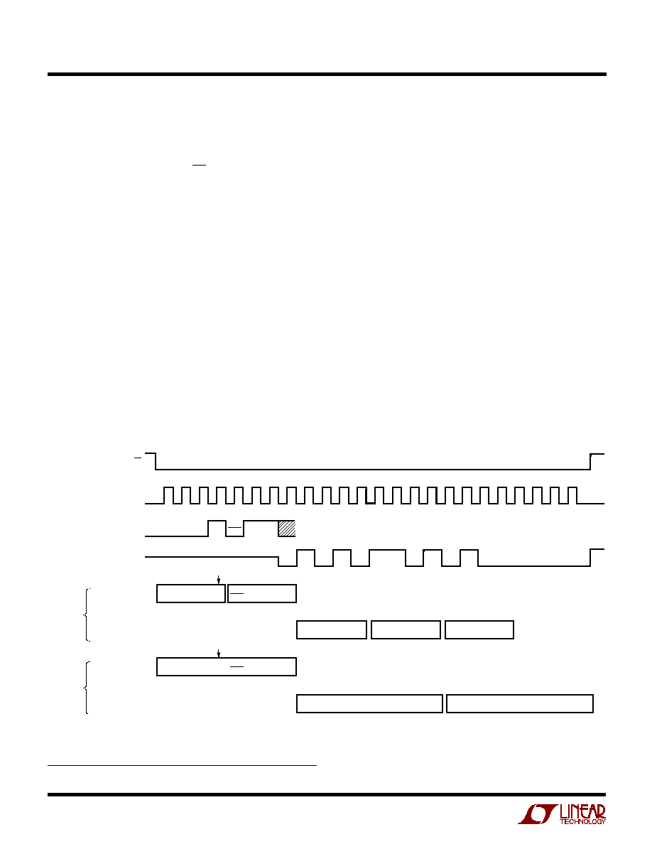
The LTC1091/LTC1093/LTC1094 communicate with
microprocessors and other external circuitry via a syn-
chronous, half-duplex, 4-wire serial interface while the
LTC1092 uses a 3-wire interface (see Operating Sequence).
The clock (CLK) synchronizes the data transfer with each
bit being transmitted on the falling CLK edge and captured
on the rising CLK edge in both transmitting and receiving
systems. The LTC1091/LTC1093/LTC1094 first receive
input data and then transmit back the A/D conversion
result (half-duplex). Because of the half-duplex operation,
D
IN
and D
OUT
may be tied together allowing transmission
over just three wires: CS, CLK and DATA (D
IN
/D
OUT
).
Data transfer is initiated by a falling chip select (CS) signal.
After CS falls, the LTC1091/LTC1093/LTC1094 looks for a
start bit. After the start bit is received, a 3-bit input word
(6 bits for the LTC1093/LTC1094) is shifted into the D
IN
input which configures the LTC1091/LTC1093/LTC1094
and starts the conversion. After one null bit, the result of
the conversion is output on the D
OUT
line. At the end of the
data exchange, CS should be brought high. This resets the
LTC1091/LTC1093/LTC1094 in preparation for the next
data exchange.
The LTC1092 does not require a configuration input word
and has no D
IN
pin. A falling CS initiates data transfer as
shown in the LTC1092 Operating Sequence. After CS falls,

12
LTC1091/LTC1092
LTC1093/LTC1094
U
S
A
O
PPLICATI
W
U
U
I FOR ATIO
D
IN
1
D
IN
2
D
OUT
1
D
OUT
2
CS
SHIFT MUX
ADDRESS IN
1 NULL BIT
SHIFT A/D CONVERSION
RESULT OUT
1091/2/3/4 AI01
the first CLK pulse enables D
OUT
. After one null bit, the A/D
conversion result is output on the D
OUT
line. Bringing CS
high resets the LTC1092 for the next data exchange.
2. Input Data Word
The LTC1092 requires no D
IN
word. It is permanently
configured to have a single differential input and to operate
in unipolar mode. The conversion result is output on the
D
OUT
line in MSB-first sequence, followed by LSB-first
sequence, providing easy interface to MSB- or LSB-first
serial ports. The following disussion applies to the con-
figuration of the LTC1091/LTC1093/LTC1094.
The LTC1091/LTC1093/LTC1094 clock data into the D
IN
input on the rising edge of the clock. The input data words
are defined as follows:
SELECT
1
START
SELECT
0
UNI
MSBF
MUX ADDRESS
LTC1093/LTC1094 DATA INPUT (D
IN
)WORD:
MSB-FIRST/
LSB-FIRST
UNIPOLAR/
BIPOLAR
1091/2/3/4 AI02
ODD/
SIGN
SGL/
DIFF
START
MSBF
MUX ADDRESS
LTC1091 DATA INPUT (D
IN
) WORD:
MSB-FIRST/
LSB-FIRST
ODD/
SIGN
SGL/
DIFF
t
CONV
tCYC
tSMPL
Hi-Z
FILLED WITH ZEROS
1091/2/3/4 AI03
CLK
START
Hi-Z
ODD/SIGN
MSBF
SGL/
DIFF
DIN
DOUT
CS
B1
B9
B0
DON'T CARE
t
CONV
tCYC
tSMPL
Hi-Z
FILLED WITH
ZEROS
1091/2/3/4 AI04
CLK
START
Hi-Z
ODD/SIGN
MSBF
SGL/
DIFF
DIN
DOUT
CS
B1
B9
B0
B1
B9
DON'T CARE
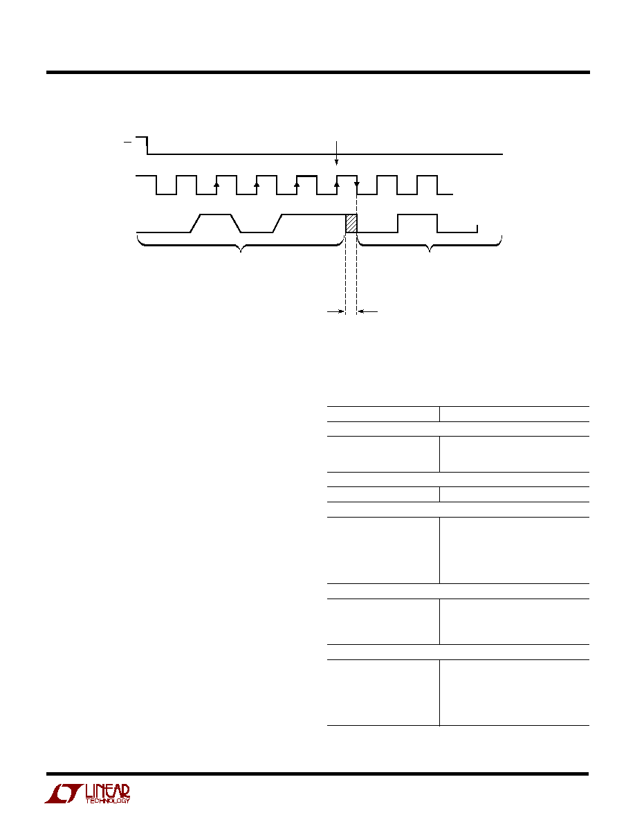
LTC1091 Operating Sequence
Example: Differential Inputs (CH1
+
, CH0
≠
)
MSB-First Data (MSBF = 1)
LSB-First Data (MSBF = 0)

13
LTC1091/LTC1092
LTC1093/LTC1094
U
S
A
O
PPLICATI
W
U
U
I FOR ATIO
LTC1092 Operating Sequence
t
CONV
t
CYC
t
SMPL
Hi-Z
FILLED WITH ZEROS
1091/2/3/4 AI06
CLK
START
Hi-Z
UNI
SEL1
SEL0
MSBF
SGL/
DIFF
ODD/
SIGN
D
IN
D
OUT
CS
B1
B9
B0
DON'T CARE
t
CONV
tCYC
tSMPL
Hi-Z
FILLED WITH
ZEROS
1091/2/3/4 AI07
CLK
START
Hi-Z
Hi-Z
UNI
SEL1
SEL0
MSBF
SGL/
DIFF
ODD/
SIGN
DIN
DOUT
CS
B1
B9
B0
DON'T CARE
B9
B1
LTC1093/LTC1094 Operating Sequence
Example: Differential Inputs (CH4
+
, CH5
≠
), Unipolar Mode
MSB-First Data (MSBF = 1)
LSB-First Data (MSBF = 0)
t
CONV
tCYC
tSMPL
tSMPL
1091/2/3/4 AI05
CLK
Hi-Z
DOUT
CS
B1
B9
B9
B0
B1
14
LTC1091/LTC1092
LTC1093/LTC1094
U
S
A
O
PPLICATI
W
U
U
I FOR ATIO
Start Bit
The first "logical one" clocked into the D
IN
input after CS
goes low is the start bit. The start bit initiates the data
transfer. The LTC1091/LTC1093/LTC1094 will ignore all
leading zeros which precede this logical one. After the start
bit is received, the remaining bits of the input word will be
clocked in. Further inputs on the D
IN
pin are then ignored
until the next CS cycle.
Multiplexer (MUX) Address
The bits of the input word following the START bit assign
the MUX configuration for the requested conversion. For
a given channel selection, the converter will measure the
voltage between the two channels indicated by the + and
≠ signs in the selected row of the following tables. In
single-ended mode, all input channels are measured with
respect to GND on the LTC1091 and COM on the
LTC1093/LTC1094.
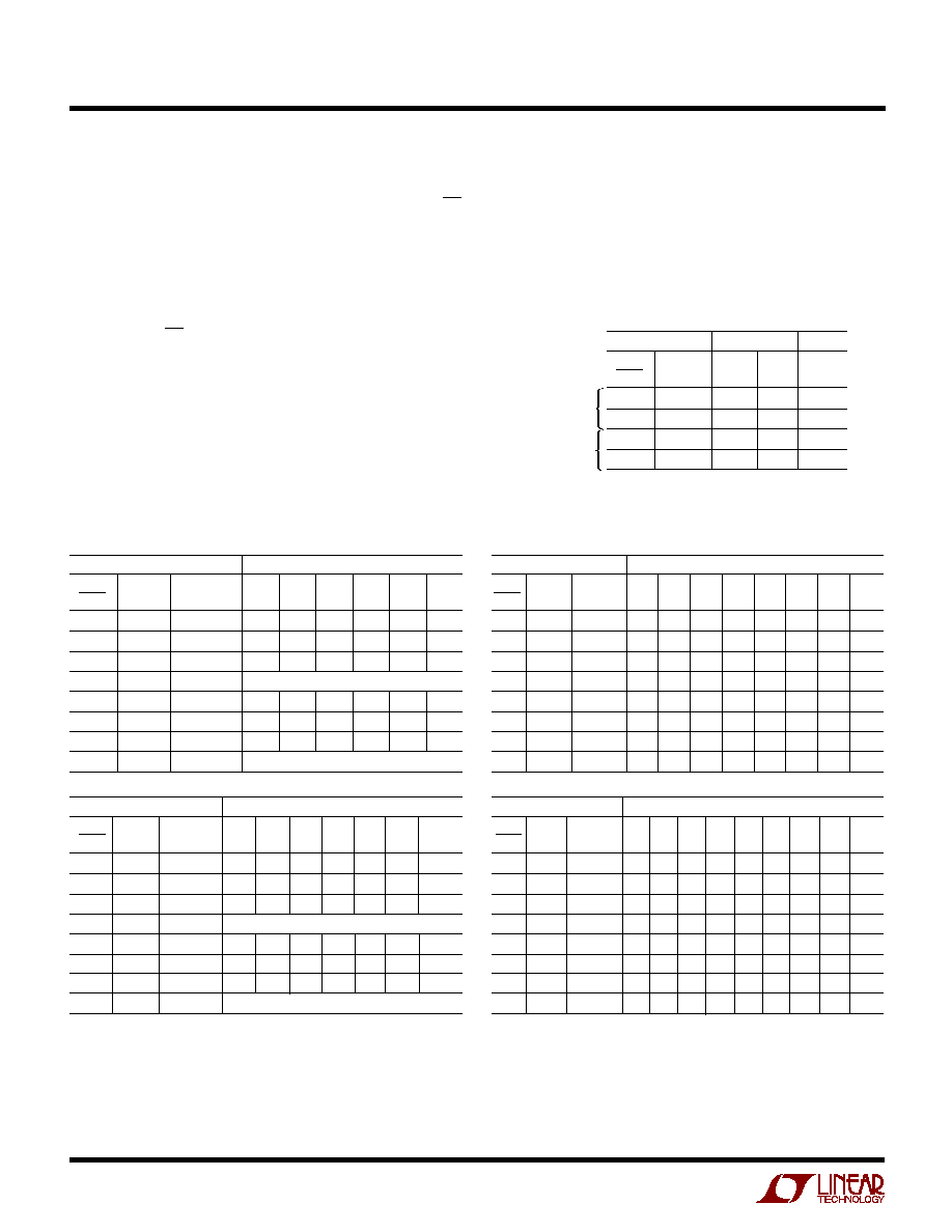
SINGLE-ENDED
MUX MODE
MUX ADDRESS
CHANNEL #
GND
DIFFERENTIAL
MUX MODE
SGL/
DIFF
1
1
0
0
ODD/
SIGN
0
1
0
1
0
+
+
≠
1
+
≠
+
≠
≠
1091-4 AI08
LTC1091 Channel Selection
MUX ADDRESS
SELECT
DIFFERENTIAL CHANNEL SELECTION
SGL/
DIFF
0
0
0
0
0
0
0
0
ODD/
SIGN
0
0
0
0
1
1
1
1
1
0
0
1
1
0
0
1
1
0
0
1
0
1
0
1
0
1
0
+
≠
1
≠
+
2
+
≠
3
≠
+
4
+
≠
5
≠
+
1091-4 AI09
NOT USED
NOT USED
MUX ADDRESS
SELECT
SINGLE-ENDED CHANNEL SELECTION
SGL/
DIFF
1
1
1
1
1
1
1
1
ODD/
SIGN
0
0
0
0
1
1
1
1
1
0
0
1
1
0
0
1
1
0
0
1
0
1
0
1
0
1
0
+
1
+
2
+
3
+
4
+
5
+
COM
≠
≠
≠
≠
≠
≠
NOT USED
NOT USED
LTC1093 Channel Selection
MUX ADDRESS
SELECT
DIFFERENTIAL CHANNEL SELECTION
SGL/
DIFF
0
0
0
0
0
0
0
0
ODD/
SIGN
0
0
0
0
1
1
1
1
1
0
0
1
1
0
0
1
1
0
0
1
0
1
0
1
0
1
0
+
≠
1
≠
+
2
+
≠
3
≠
+
4
+
≠
5
≠
+
6
+
≠
7
≠
+
1091-4 AI0
MUX ADDRESS
SELECT
SINGLE-ENDED CHANNEL SELECTION
SGL/
DIFF
1
1
1
1
1
1
1
1
1
0
0
1
1
0
0
1
1
0
0
1
0
1
0
1
0
1
0
+
1
+
2
+
3
+
4
+
5
+
6
+
7
+
COM
≠
≠
≠
≠
≠
≠
≠
≠
ODD/
SIGN
0
0
0
0
1
1
1
1
LTC1094 Channel Selection
15
LTC1091/LTC1092
LTC1093/LTC1094
U
S
A
O
PPLICATI
W
U
U
I FOR ATIO
Unipolar Transfer Curve (UNI = 1)
MSB-First/LSB-First (MSBF)
The output data of the LTC1091/LTC1093/LTC1094 is
programmed for MSB-first or LSB-first sequence using
the MSBF bit. When the MSBF bit is a logical one, data will
appear on the D
OUT
line in MSB-first format. Logical zeros
will be filled in indefinitely following the last data bit to
accommodate longer word lengths required by some
microprocessors. When the MSBF bit is a logical zero,
LSB-first data will follow the normal MSB-first data on the
D
OUT
line. (See operating sequence).
Unipolar/Bipolar (UNI)
The UNI bit of the LTC1093/LTC1094 determines whether
the conversion will be unipolar or bipolar. When UNI is a
logical one, a unipolar conversion will be performed on the
selected input voltage. When UNI is a logical zero, a bipolar
conversion will result. The input span and code assign-
ment for each conversion type are shown in the figures
below.
The LTC1091/LTC1092 are permanently configured for
unipolar mode.
0V
1LSB
V
REF
≠ 2LSB
V
REF
≠ 1LSB
V
REF
V
IN
0 0 0 0 0 0 0 0 0 1
0 0 0 0 0 0 0 0 0 0
1 1 1 1 1 1 1 1 1 1
1 1 1 1 1 1 1 1 1 0
1091-4 AI11
1LSB
V
REF
≠ 2LSB
V
REF
≠ 1LSB
V
REF
V
IN
1 1 1 1 1 1 1 1 1 1
0 0 0 0 0 0 0 0 0 1
0 0 0 0 0 0 0 0 0 0
0 1 1 1 1 1 1 1 1 0
0 1 1 1 1 1 1 1 1 1
1 1 1 1 1 1 1 1 1 0
1 0 0 0 0 0 0 0 0 1
1 0 0 0 0 0 0 0 0 0
≠1LSB
≠2LSB
≠V
REF
≠V
REF
+ 1LSB
1091-4 AI12
OUTPUT CODE
1 1 1 1 1 1 1 1 1 1
1 1 1 1 1 1 1 1 1 0
∑
∑
∑
0 0 0 0 0 0 0 0 0 1
0 0 0 0 0 0 0 0 0 0
INPUT VOLTAGE
V
REF
≠ 1LSB
V
REF
≠ 2LSB
∑
∑
∑
1LSB
0V
INPUT VOLTAGE
(V
REF
= 5V)
4.9951V
4.9902V
∑
∑
∑
0.0049V
0V
1091-4AI13
Bipolar Transfer Curve (UNI = 0) LTC1093/LTC1094 Only
Unipolar Output Code (UNI = 1)
OUTPUT CODE
0 1 1 1 1 1 1 1 1 1
0 1 1 1 1 1 1 1 1 0
∑
∑
∑
0 0 0 0 0 0 0 0 0 1
0 0 0 0 0 0 0 0 0 0
1 1 1 1 1 1 1 1 1 1
1 1 1 1 1 1 1 1 1 0
∑
∑
∑
1 0 0 0 0 0 0 0 0 1
1 0 0 0 0 0 0 0 0 0
INPUT VOLTAGE
V
REF
≠ 1LSB
V
REF
≠ 2LSB
∑
∑
∑
1LSB
0V
≠1LSB
≠2LSB
∑
∑
∑
≠(V
REF
) + 1LSB
≠(V
REF
)
INPUT VOLTAGE
(V
REF
= 5V)
4.9902V
4.9805V
∑
∑
∑
0.0098V
0V
≠0.0098V
≠0.0195V
∑
∑
∑
≠4.9902V
≠5.000V
1091-4AI14
Bipolar Output Code (UNI = 0) LTC1093/LTC1094 Only
16
LTC1091/LTC1092
LTC1093/LTC1094
U
S
A
O
PPLICATI
W
U
U
I FOR ATIO
3. Accommodating Microprocessors with
Different Word Lengths
The LTC1091/LTC1093/LTC1094 will fill zeros indefinitely
after the transmitted data until CS is brought high. At that
time the D
OUT
line is disabled. This makes interfacing easy
to MPU serial ports with different transfer increments
including 4 bits (e.g., COP400) and 8 bits (e.g., SPI and
MICROWIRE/PLUS
TM
). Any word length can be accommo-
dated by the correct positioning of the start bit in the
LTC1091 input word.
Figure 1 shows examples of LTC1091 input and output
words for 4-bit and 8-bit processors. A complete data
exchange can be implemented with two 4-bit MPU outputs
and three inputs in 4-bit systems and one 8-bit output and
two inputs in 8-bit systems. The resulting data winds up
left justified in the MPU with zeros automatically filled in
the unused low order bits by the LTC1091. In section 5
another example is given using the MC68HC05C4 which
MICROWIRE/PLUS is a trademark of National Semiconductor Corp.
eliminates one 8-bit transfer and positions data right
justified inside the MPU.
4. Operation with D
IN
and D
OUT
Tied Together
The LTC1091/LTC1093/LTC1094 can be operated with
D
IN
and D
OUT
tied together. This eliminates one of the lines
required to communicate to the MPU. Data is transmitted
in both directions on a single wire. The processor pin
connected to this data line should be configurable as either
an input or an output. The LTC1091, for example, will take
control of the data line and drive it low on the 4th falling
CLK edge after the start bit is received (see Figure 2).
Therefore, the processor port line must be switched to an
input before this happens, to avoid a conflict.
In the next section, an example is made of interfacing
the LTC1091 with D
IN
and D
OUT
tied together to the Intel
8051 MPU.
FILL ZEROS
X = DON'T CARE
1091/2/3/4 F01
CLK
CS
D
OUT
MPU SENDS
2 D
IN
WORDS
4-BIT
TRANSFERS
MPU READS BACK
3 D
OUT
WORDS
START
BIT
D
IN
Hi-Z
START
MSBF
MSBF X
0 0 0 1
∑ ∑ ∑
B9
B8
B7
B6
B5
B4
B3
B2
B1
B0
SGL/
DIFF
ODD/
SIGN
SGL/
DIFF
ODD/
SIGN
MSBF X
SGL/
DIFF
ODD/
SIGN
B9 B8 B7 B6
B5 B4 B3 B2
B1 B0 0 0
B9 B8 B7 B6
B5 B4 B3 B2
B1 B0 0 0 0 0 0 0
START
BIT
0 0 0 1
MPU SENDS
1 D
IN
WORD
8-BIT
TRANSFERS
MPU READS BACK
2 D
OUT
WORDS
Figure 1. LTC1091 Input and Output Word Arrangements for 4-Bit and 8-Bit Serial Port Microprocessors
17
LTC1091/LTC1092
LTC1093/LTC1094
U
S
A
O
PPLICATI
W
U
U
I FOR ATIO
MICROWIRE is a trademark of National Semiconductor Corp.
Table 1. Microprocessors with Hardware Serial Interfaces
Compatible with the LTC1091/LTC1092/LTC1093/LTC1094
PART NUMBER
TYPE OF INTERFACE
Motorola
MC6805S2, S3
SPI
MC68HC11
SPI
MC68HC05
SPI
RCA
CDP68HC05
SPI
Hitachi
HD6305
SCI Synchronous
HD63705
SCI Synchronous
HD6301
SCI Synchronous
HD63701
SCI Synchronous
HD6303
SCI Synchronous
HD64180
CSI/O
National Semiconductor
COP400 Family
MICROWIRE
TM
COP800 Family
MICROWIRE/PLUS
NS8050U
MICROWIRE/PLUS
HPC16000 Family
MICROWIRE/PLUS
Texas Instruments
TMS7002
Serial Port
TMS7042
Serial Port
TMS70C02
Serial Port
TMS70C42
Serial Port
TMS32011*
Serial Port
TMS32020
Serial Port
*Requires external hardware
5. Microprocessor Interfaces
The LTC1091/LTC1092/LTC1093/LTC1094 can interface
directly (without external hardware) to most popular
microprocessor (MPU) synchronous serial formats (see
Table 1). If an MPU without a dedicated serial port is used,
then three or four of the MPU's parallel port lines can be
programmed to form the serial link to the LTC1091/
LTC1092/LTC1093/LTC1094. Included here are one serial
interface example and one example showing a parallel port
programmed to form the serial interface.
1091/2/3/4 F02
CLK
START
MSBF
B9
B8
∑ ∑ ∑
PROCESSOR
MUST RELEASE
DATA LINE AFTER 4TH
RISING CLK AND BEFORE
THE 4TH FALLING CLK
MPU CONTROLS
DATA LINE AND SENDS
MUX ADDRESS TO LTC1091
LTC1091 TAKES CONTROL OF DATA LINE
ON 4TH FALLING CLK
SGL/
DIFF
ODD/
SIGN
CS
DATA (D
IN
/D
OUT
)
1
2
MSBF
LATCHED
BY LTC1091
3
4
LTC1091 CONTROLS
DATA LINE AND SENDS
A/D RESULT BACK TO MPU
Figure 2. LTC1091 Operation with D
IN
and D
OUT
Tied Together
18
LTC1091/LTC1092
LTC1093/LTC1094
U
S
A
O
PPLICATI
W
U
U
I FOR ATIO
Hardware and Software Interface to
Motorola MC68HC05C4 Processor
Motorola SPI (MC68HC05C4, MC68HC11)
The MC68HC05C4 has been chosen as an example of an
MPU with a dedicated serial port. This MPU transfers data
MSB first and in 8-bit increments. With two 8-bit transfers,
the A/D result is read into the MPU. The first 8-bit transfer
sends the D
IN
word to the LTC1091 and clocks B9 and B8
of the A/D conversion result into the processor. The
second 8-bit transfer clocks the remaining bits, B7 through
B0, into the MPU.
ANDing the first MPU received byte with 03 Hex clears the
six most significant bits. Notice how the position of the
start bit in the first MPU transmit word is used to position
the A/D result right justified in two memory locations.
X = DON'T CARE
1091/2/3/4 AI15
CLK
CS
D
OUT
MPU RECEIVED
WORD
MPU TRANSMIT
WORD
START
BIT
BYTE 1
D
IN
START
MSBF
MSBF X X X
B9
?
?
?
0
B9
B8
B8
B7
B6
B5
B4
B3
B2
B1
B0
SGL/
DIFF
ODD/
SIGN
SGL/
DIFF
ODD/
SIGN
0 1
BYTE 2 (DUMMY)
X X X
X X X
X X
BYTE 1
1ST TRANSFER
? ?
BYTE 2
B5 B4 B3
B2 B1 B0
B7 B6
DON'T CARE
2ND TRANSFER
Data Exchange Between LTC1091 and MC68HC05C4
1091-4 AI16
BYTE 1
0 0 0 0 0 0 B9 B8
D
OUT
from LTC1091 Stored in MC68HC05C4 RAM
MSB
LOCATION A
B7 B6 B5 B4 B3 B2 B1 B0
LSB
LOCATION A + 1
BYTE 2
LTC1091
CS
CLK
DIN
DOUT
ANALOG
INPUTS
CO
SCK
MOSI
MISO
MC68HC05C4
LABEL
MNEMONIC
COMMENTS
START
BCLRn
Bit 0 Port C Goes Low (CS Goes Low)
LDA
Load LTC1090 D
IN
Word into Acc
STA
Load LTC1090 D
IN
Word into SPI from Acc
Transfer Begins
TST
Test Status of SPIF
BPL
Loop to Previous Instruction If Not Done
with Transfer
LDA
Load contents of SPI Data Register into
Acc (D
OUT
MSBs)
STA
Start Next SPI Cycle
AND
Clear 6 MSBs of First D
OUT
Word
STA
Store in Memory Location A (MSBs)
TST
Test Status of SPIF
BPL
Loop to Previous Instruction If Not Done
with Transfer
BSETn
Set B0 of Port C (CS Goes High)
LDA
Load contents of SPI Data Register into
Acc (D
OUT
LSBs)
STA
Store in Memory location A + 1 (LSBs)
19
LTC1091/LTC1092
LTC1093/LTC1094
U
S
A
O
PPLICATI
W
U
U
I FOR ATIO
Interfacing to the Parallel Port of the
Intel 8051 Family
The Intel 8051 has been chosen to demonstrate the
interface between the LTC1091 and parallel port micro-
processors. Normally, the CS, SCLK and D
IN
signals
would be generated on three port lines and the D
OUT
signal
read on a 4th port line. This works very well. However, we
will demonstrate here an interface with the D
IN
and D
OUT
of the LTC1091 tied together as described in section 4.
This saves one wire.
The 8051 first sends the start bit and MUX address to the
LTC1091 over the data line connected to P1.2. Then P1.2
is reconfigured as an input (by writing to it a one) and the
8051 reads back the 10-bit A/D result over the same data
line.
1091-4 AI17
LTC1091
CS
CLK
DOUT
DIN
ANALOG
INPUTS
P1.4
P1.3
P1.2
8051
MUX ADDRESS
A/D RESULT
B9 B8 B7 B6 B5 B4 B3 B2
D
OUT
from LTC1091 Stored in 8051 RAM
MSB
R2
B1 B0 0 0 0 0 0 0
LSB
R3
LABEL
MNEMONIC
OPERAND
COMMENTS
MOV
A, #FFH
D
IN
Word for LTC1091
SETB
P1.4
Make Sure CS Is High
CLR
P1.4
CS Goes Low
MOV
R4, #04
Load Counter
LOOP 1 RLC
A
Rotate D
IN
Bit into Carry
CLR
P1.3
SCLK Goes Low
MOV
P1.2, C
Output D
IN
Bit to LTC1091
SETB
P1.3
SCLK Goes High
DJNZ
R4, LOOP 1
Next Bit
MOV
P1, #04
Bit 2 Becomes an Input
CLR
P1.3
SCLK Goes Low
MOV
R4, #09
Load Counter
LOOP
MOV
C, P1.2
Read Data Bit into Carry
RLC
A
Rotate Data Bit into Acc
SETB
P1.3
SCLK Goes High
CLR
P1.3
SCLK Goes Low
DJNZ
R4, LOOP
Next Bit
MOV
R2, A
Store MSBs in R2
MOV
C, P1.2
Read Data Bit into Carry
SETB
P1.3
SCLK Goes High
CLR
P1.3
SCLK Goes Low
CLR
A
Clear Acc
RLC
A
Rotate Data Bit from Carry to Acc
MOV
C, P1.2
Read Data Bit into Carry
RRC
A
Rotate Right into Acc
RRC
A
Rotate Right into Acc
MOV
R3, A
Store LSBs in R3
SETB
P1.4
CS Goes High
1091/2/3/4 AI18
CLK
START
MSBF
B9
B8
B7
B6
B5
B4
B3
B2
B1
B0
8051 P1.2 RECONFIGURED AS AN
INPUT AFTER THE 4TH RISING CLK
AND BEFORE THE 4TH FALLING CLK
8051 P1.2 OUTPUTS
DATA TO LTC1091
LTC1091 TAKES CONTROL OF DATA LINE
ON 4TH FALLING CLK
SGL/
DIFF
ODD/
SIGN
CS
DATA (D
IN
/D
OUT
)
1
2
MSBF BIT
LATCHED
INTO LTC1091
3
4
LTC1091 SENDS A/D RESULT
BACK TO 8051 P1.2
20
LTC1091/LTC1092
LTC1093/LTC1094
U
S
A
O
PPLICATI
W
U
U
I FOR ATIO
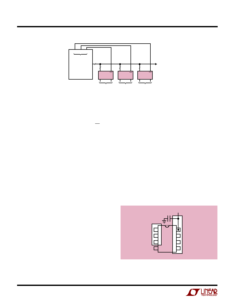
Figure 3. Several LTC1094s Sharing One 3-Wire Serial Interface
8 CHANNELS
8 CHANNELS
8 CHANNELS
3
3
3
3
3-WIRE SERIAL
INTERFACE TO OTHER
PERIPHERALS OR LTC1094s
2
1
0
OUTPUT PORT
SERIAL DATA
MPU
LTC1091-4 F03
LTC1094
CS
LTC1094
CS
LTC1094
CS
Sharing the Serial Interface
The LTC1094 can share the same 2- or 3-wire serial
interface with other peripheral components or other
LTC1094s (see Figure 3). In this case, the CS signals
decide which LTC1094 is being addressed by the MPU.
ANALOG CONSIDERATIONS
1. Grounding
The LTC1091/LTC1092/LTC1093/LTC1094 should be used
with an analog ground plane and single point grounding
techniques.
The AGND pin (GND on the LTC1091/LTC1092) should be
tied directly to this ground plane.
The DGND pin of the LTC1093/LTC1094 can also be tied
directly to this ground plane because minimal digital noise
is generated within the chip itself.
The V
CC
pin should be bypassed to the ground plane with
a 4.7
µ
F tantalum with leads as short as possible. AV
CC
and
DV
CC
should be tied together on the LTC1094. The V
≠
pin
(LTC1093/LTC1094) should be bypassed with a 0.1
µ
F
ceramic disk. For single supply applications, V
≠
can be
tied to the ground plane.
It is also recommended that the REF
≠
pin and the COM pin
be tied directly to the ground plane. All analog inputs
should be referenced directly to the single point ground.
Digital inputs and outputs should be shielded from and/or
routed away from the reference and analog circuitry.
Figure 4. Example Ground Plane for the LTC1091
Figure 4 shows an example of an ideal LTC1091 ground
plane design for a 2-sided board. Of course, this much
ground plane will not always be possible, but users should
strive to get as close to this ideal as possible.
2. Bypassing
For good performance, V
CC
must be free of noise and
ripple. Any changes in the V
CC
voltage with respect to
analog ground during a conversion cycle can induce
errors or noise in the output code. Because the V
CC
(V
REF
)
pin of the LTC1091 defines the voltage span of the A/D
converter, its bypassing is especially important. V
CC
noise
and ripple can be kept below 1mV by bypassing the V
CC
pin
directly to the analog ground plane with a 4.7
µ
F tantalum
with leads as short as possible. AV
CC
and DV
CC
should be
tied together on the LTC1094. Figures 5 and 6 show the
effects of good and poor V
CC
bypassing.
1
2
3
4
S
S
8
7
6
5
4.7
µ
F
TANTALUM
V
CC
LTC1091-4 F04

21
LTC1091/LTC1092
LTC1093/LTC1094
U
S
A
O
PPLICATI
W
U
U
I FOR ATIO
3. Analog Inputs
Because of the capacitive redistribution A/D conversion
techniques used, the analog inputs of the LTC1091/
LTC1092/LTC1093/LTC1094 have capacitive switching
input current spikes. These current spikes settle quickly
and do not cause a problem. However, if large source
resistances are used or if slow settling op amps drive the
inputs, care must be taken to ensure that the transients
caused by the current spikes settle completely before the
conversion begins.
Source Resistance
The analog inputs of the LTC1091/LTC1092/LTC1093/
LTC1094 look like a 60pF capacitor (C
IN
) in series with a
500
resistor (R
ON
) as shown in Figure 7. C
IN
gets
switched between the selected "+" and "≠" inputs once
during each conversion cycle. Large external source resis-
tors and capacitances will slow the settling of the inputs. It
is important that the overall RC time constants be short
enough to allow the analog inputs to completely settle
within the allowed time.
"+" Input Settling
This input capacitor is switched onto the "+" input during
the sample phase (t
SMPL
, see Figure 8). The sample phase
is the 1 1/2 CLK cycles before the conversion starts. The
voltage on the "+" input must settle completely within this
sample time. Minimizing R
SOURCE
+
and C1 will improve
the input settling time. If large "+" input source resistance
must be used, the sample time can be increased by using
a slower CLK frequency. With the minimum possible
sample time of 3
µ
s, R
SOURCE
+
< 2k and C1 < 20pF will
provide adequate settling.
Figure 5. Poor V
CC
Bypassing.
Noise and Ripple Can Cause A/D Errors
10
µ
s/DIV
1091-4 F05
0.5mV/DIV
Figure 6. Good V
CC
Bypassing Keeps
Noise and Ripple on V
CC
Below 1mV
0.5mV/DIV
10
µ
s/DIV
1091-4 F06
3RD CLK
R
ON
= 500
4TH CLK
C
IN
=
60pF
LTC1091
"+"
INPUT
R
SOURCE
+
V
IN
+
C1
"≠"
INPUT
R
SOURCE
≠
V
IN
≠
C2
LTC091-4 F07
Figure 7. Analog Input Equivalent Circuit

22
LTC1091/LTC1092
LTC1093/LTC1094
U
S
A
O
PPLICATI
W
U
U
I FOR ATIO
Figure 8. "+" and "≠" Input Settling Windows
"≠" Input Settling
At the end of the sample phase the input capacitor switches
to the "≠" input and the conversion starts (see Figure 8).
During the conversion, the "+" input voltage is effectively
"held" by the sample-and-hold and will not affect the
conversion result. However, it is critical that the "≠" input
voltage settle completely during the first CLK cycle of the
conversion time and be free of noise. Minimizing R
SOURCE
≠
and C2 will improve settling time. If large "≠" input source
resistance must be used, the time allowed for settling can
be extended by using a slower CLK frequency. At the
maximum CLK rate of 500kHz, R
SOURCE
≠
< 1k
and
C2 < 20pF will provide adequate settling.
Input Op Amps
When driving the analog inputs with an op amp it is
important that the op amp settle within the allowed time
(see Figure 8). Again, the "+" and "≠" input sampling times
can be extended as previously described to accommodate
slower op amps. Most op amps, including the LT1006 and
LT1013 single supply op amps, can be made to settle well
even with the minimum settling windows of 3
µ
s ("+"
input) and 2
µ
s ("≠" input) which occur at the maximum
clock rate of 500kHz. Figures 9 and 10 show examples of
adequate and poor op amp settling.
CLK
D
IN
D
OUT
"+" INPUT
"≠" INPUT
SAMPLE
HOLD
"+" INPUT MUST
SETTLE DURING
THIS TIME
t
SMPL
t
CONV
CS
SGL/DIFF
START
MSBF
B9
1ST BIT TEST "≠" INPUT MUST
SETTLE DURING THIS TIME
1091-4 F08
DON`T CARE

23
LTC1091/LTC1092
LTC1093/LTC1094
U
S
A
O
PPLICATI
W
U
U
I FOR ATIO
Figure 10. Poor Op Amp Settling Can Cause A/D Errors
Figure 9. Adequate Settling of Op Amp Driving Analog Input
5mV/DIV
1
µ
s/DIV
1091-4 F09
5mV/DIV
20
µ
s/DIV
1091-4 F10
RC Input Filtering
It is possible to filter the inputs with an RC network as
shown in Figure 11. For large values of C
F
(e.g., 1
µ
F), the
capacitive input switching currents are averaged into a net
DC current. Therefore, a filter should be chosen with a small
resistor and large capacitor to prevent DC drops across the
resistor. The magnitude of the DC current is approximately
I
DC
= (60pF)(V
IN
/t
CYC
) and is roughly proportional to V
IN
.
When running at the minimum cycle time of 32
µ
s, the input
current equals 9
µ
A at V
IN
= 5V. In this case, a filter resistor
of 50
will cause 0.1LSB of full-scale error. If a larger filter
resistor must be used, errors can be eliminated by increas-
ing the cycle time as shown in the typical curve of Maximum
Filter Resistor vs Cycle Time.
Input Leakage Current
Input leakage currents can also create errors if the source
resistance gets too large. For instance, the maximum input
leakage specification of 1
µ
A (at 125
∞
C) flowing through a
source resistance of 1k
will cause a voltage drop of 1mV
or 0.2LSB. This error will be much reduced at lower
temperatures because leakage drops rapidly (see the
typical curve of Input Channel Leakage Current vs
Temperature).
4. Sample-and-Hold
Single-Ended Inputs
The LTC1091/LTC1093/LTC1094 provide a built-in sample-
and-hold (S&H) function for all signals acquired in the single-
ended mode. This sample-and-hold allows conversion of
rapidly varying signals (see typical curve of S&H Acquisition
Time vs Source Resistance). The input voltage is sampled
during the t
SMPL
time as shown in Figure 8. The sampling
interval begins as the bit preceding the MSBF bit is shifted in
and continues until the falling CLK edge after the MSBF bit is
received. On this falling edge, the S&H goes into hold mode
and the conversion begins.
Figure 11. RC Input Filtering
R
FILTER
V
IN
C
FILTER
1091-4 F11
LTC1091
"+"
"≠"
I
DC
24
LTC1091/LTC1092
LTC1093/LTC1094
Figure 12. Reference Input Equivalent Circuit
U
S
A
O
PPLICATI
W
U
U
I FOR ATIO
Differential Inputs
With differential inputs, the A/D no longer converts just a
single voltage but rather the difference between two volt-
ages. In this case, the voltage on the selected "+" input is still
sampled and held and therefore may be rapidly time varying
just as in single-ended mode. However, the voltage on the
selected "≠" input must remain constant and be free of noise
and ripple throughout the conversion time. Otherwise, the
differencing operation may not be performed accurately.
The conversion time is 10 CLK cycles. Therefore, a change
in the "≠" input voltage during this interval can cause
conversion errors. For a sinusoidal voltage on the "≠" input
this error would be:
V
ERROR(MAX)
= (V
PEAK
)(2
) ∑ f("≠")(10/f
CLK
)
Where f("≠") is the frequency of the "≠" input voltage,
V
PEAK
is its peak amplitude and f
CLK
is the frequency of the
CLK. In most cases V
ERROR
will not be significant. For a
60Hz signal on the "≠" input to generate a 0.25LSB error
(1.25mV) with the converter running at CLK = 500kHz, its
peak value would have to be 150mV.
5. Reference Inputs
The voltage between the reference inputs of the
LTC1091/LTC1092/LTC1093/LTC1094 defines the volt-
age span of the A/D converter. The reference inputs look
primarily like a 10k resistor but will have transient capaci-
tive switching currents due to the switched capacitor
conversion technique (see Figure 12). During each bit test
of the conversion (every CLK cycle), a capacitive current
spike will be generated on the reference pins by the A/D.
These current spikes settle quickly and do not cause a
problem. However, if slow settling circuitry is used to drive
the reference inputs, care must be taken to ensure that
transients caused by these current spikes settle com-
pletely during each bit test of the conversion.
When driving the reference inputs, three things should be
kept in mind:
1. The source resistance (R
OUT
) driving the reference
inputs should be low (less than 1
) to prevent DC
drops caused by the 1mA maximum reference current
(I
REF
).
2. Transients on the reference inputs caused by the
capacitive switching currents must settle completely
during each bit test (each CLK cycle). Figures 13 and
14 show examples of both adequate and poor settling.
Using a slower CLK will allow more time for the
reference to settle. However, even at the maximum
CLK rate of 500kHz most references and op amps can
be made to settle within the 2
µ
s bit time.
3. It is recommended that the REF
≠
input of the LTC1094
be tied directly to the analog ground plane. If REF
≠
is
biased at a voltage other than ground, the voltage must
not change during a conversion cycle. This voltage
must also be free of noise and ripple with respect to
analog ground.
R
ON
5pF TO
30pF
10k
TYP
LTC1091/2/3/4
REF
+
R
OUT
V
REF
EVERY CLK CYCLE
14
13
(AGND)
1091-4 F12
0.5mV/DIV
1
µ
s/DIV
1091-4 F13
Figure 13. Adequate Reference Settling
25
LTC1091/LTC1092
LTC1093/LTC1094
U
S
A
O
PPLICATI
W
U
U
I FOR ATIO
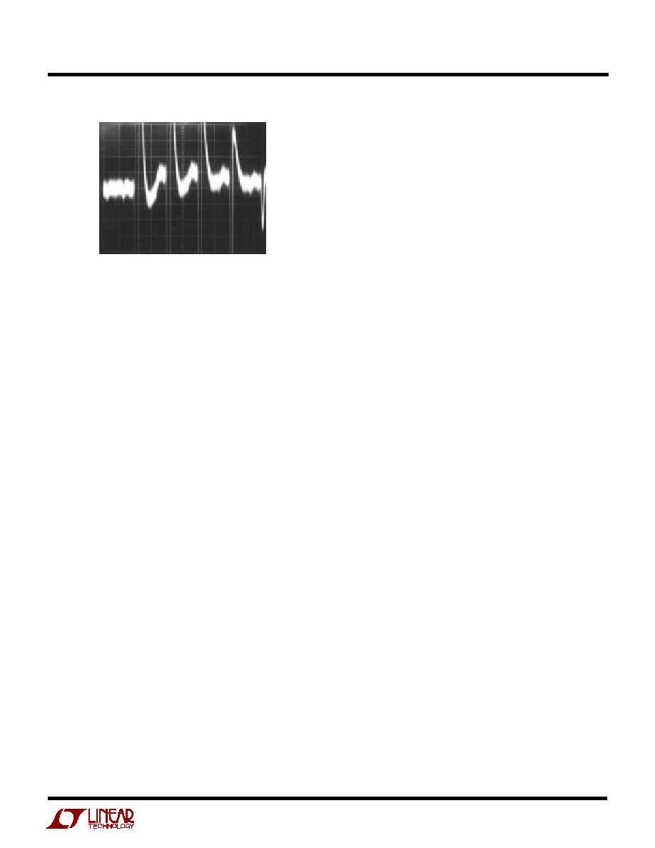
0.5mV/DIV
1
µ
s/DIV
1091-4 F14
Figure 14. Poor Reference Settling Can Cause A/D Errors
6. Reduced Reference Operation
The minimum reference voltage of the LTC1091 is limited
to 4.5V because the V
CC
supply and reference are internally
tied together. However, the LTC1092/LTC1093/LTC1094
can operate with reference voltages below 1V.
The effective resolution of the LTC1092/LTC1093/LTC1094
can be increased by reducing the input span of the con-
verter. The parts exhibit good linearity and gain over a wide
range of reference voltages (see typical curves of Linearity
and Full-Scale Error vs Reference Voltage). However, care
must be taken when operating at low values of V
REF
because of the reduced LSB step size and the resulting
higher accuracy requirement placed on the converter. The
following factors must be considered when operating at
low V
REF
values:
1. Offset
2. Noise
3. Conversion speed (CLK frequency)
Offset with Reduced V
REF
The offset of the LTC1092/LTC1093/LTC1094 has a larger
effect on the output code when the A/D is operated with
reduced reference voltage. The offset (which is typically a
fixed voltage) becomes a larger fraction of an LSB as the
size of the LSB is reduced. The typical curve of Unadjusted
Offset Error vs Reference Voltage shows how offset in
LSBs is related to reference voltage for a typical value of
V
OS
. For example, a V
OS
of 0.5mV which is 0.1LSB with a
5V reference becomes 0.5LSB with a 1V reference and
2.5LSBs with a 0.2V reference. If this offset is unaccept-
able, it can be corrected digitally by the receiving system
or by offsetting the "≠" input to the LTC1092/LTC1093/
LTC1094.
Noise with Reduced V
REF
The total input-referred noise of the LTC1092/LTC1093/
LTC1094 can be reduced to approximately 200
µ
V peak-to-
peak using a ground plane, good bypassing, good layout
techniques and minimizing noise on the reference inputs.
This noise is insignificant with a 5V reference but will
become a larger fraction of an LSB as the size of the LSB
is reduced. The typical curve of Noise Error vs Reference
Voltage shows the LSB contribution of this 200
µ
V of
noise.
For operation with a 5V reference, the 200
µ
V noise is only
0.04LSB peak-to-peak. In this case, the LTC1092/LTC1093/
LTC1094 noise will contribute virtually no uncertainty to
the output code. However, for reduced references, the
noise may become a significant fraction of an LSB and
cause undesirable jitter in the output code. For example,
with a 1V reference, this same 200
µ
V noise is 0.2LSB
peak-to-peak. This will reduce the range of input voltages
over which a stable output code can be achieved by
0.2LSB. If the reference is further reduced to 200mV, the
200
µ
V noise becomes equal to one LSB and a stable code
may be difficult to achieve. In this case averaging readings
may be necessary.
This noise data was taken in a very clean setup. Any setup-
induced noise (noise or ripple on V
CC
, V
REF
, V
IN
or V
≠
) will
add to the internal noise. The lower the reference voltage
to be used, the more critical it becomes to have a clean,
noise-free setup.
Conversion Speed with Reduced V
REF
With reduced reference voltages, the LSB step size is
reduced and the LTC1092/LTC1093/LTC1094 internal
comparator overdrive is reduced. Therefore, it may be
necessary to reduce the maximum CLK frequency when
low values of V
REF
are used.

26
LTC1091/LTC1092
LTC1093/LTC1094
U
S
A
O
PPLICATI
TYPICAL
≠
+
LTC1052
56k
TO
MCU
47
3.4k
1%
1k
0.1%
178k
0.1%
0.33
µ
F
1
µ
F
10
µ
F
1091 TA03
20k
4
1
4
4
5
6
8
6
7
3
2
2
2
8
0.1
µ
F
0.1
µ
F
CS
CH0
CH1
GND
V
CC
CLK
D
OUT
D
IN
LTC1091A
1N4148
9V
0.1
µ
F
1
µ
F
10k
+
LT1021-5
LT1025A
COMMON
V
IN
V
IN
V
OUT
GND
J TYPE
J
≠
+
0
∞
C to 500
∞
C Furnace Exhaust Gas Temperature Monitor with Low Supply Detection

27
LTC1091/LTC1092
LTC1093/LTC1094
TO
MCU
10
µ
F
V
OUT
1091 TA05
3
CS
+
≠
GND
V
CC
SCLK
D
OUT
V
REF
LTC1092
LM134 OR OTHER
1
µ
A/
∞
K SENSOR
5V
4.7
µ
F
9V
11.5k
226
LT1019-2.5
≠ 55
∞
C to 125
∞
C Thermometer Using
Current Output Silicon Sensors
CH0
CH1
CH2
CH3
CH4
CH5
CH6
CH7
COM
DGND
DV
CC
AV
CC
CLK
CS
D
OUT
D
IN
REF
+
REF
≠
AGND
V
≠
≠
+
LT1006
1491
1091-4 TA04
10k
±
10%
15k
±
10%
5V 4.7
µ
F
LTC1094
2N3904
TO
MCU
4562
2954
5000
*YSI 44007, 44034 OR EQUIVALENT
5k AT
25
∞
C
20
∞
C TO
≠40
∞
C
*
0
∞
C TO
100
∞
C
YSI 44201
YSI 44201
0
∞
C to 100
∞
C 0.25
∞
C Accurate Thermistor Based
Temperature Measurement System
U
S
A
O
PPLICATI
TYPICAL

28
LTC1091/LTC1092
LTC1093/LTC1094
PACKAGE DESCRIPTIO
U
Dimensions in inches (millimeters) unless otherwise noted.
N8 Package
8-Lead PDIP (Narrow 0.300)
(LTC DWG # 05-08-1510)
N8 1098
0.100
(2.54)
BSC
0.065
(1.651)
TYP
0.045 ≠ 0.065
(1.143 ≠ 1.651)
0.130
±
0.005
(3.302
±
0.127)
0.020
(0.508)
MIN
0.018
±
0.003
(0.457
±
0.076)
0.125
(3.175)
MIN
1
2
3
4
8
7
6
5
0.255
±
0.015*
(6.477
±
0.381)
0.400*
(10.160)
MAX
0.009 ≠ 0.015
(0.229 ≠ 0.381)
0.300 ≠ 0.325
(7.620 ≠ 8.255)
0.325
+0.035
≠0.015
+0.889
≠0.381
8.255
(
)
*THESE DIMENSIONS DO NOT INCLUDE MOLD FLASH OR PROTRUSIONS.
MOLD FLASH OR PROTRUSIONS SHALL NOT EXCEED 0.010 INCH (0.254mm)
29
LTC1091/LTC1092
LTC1093/LTC1094
PACKAGE DESCRIPTIO
U
Dimensions in inches (millimeters) unless otherwise noted.
N Package
16-Lead PDIP (Narrow 0.300)
(LTC DWG # 05-08-1510)
N16 1098
0.255
±
0.015*
(6.477
±
0.381)
0.770*
(19.558)
MAX
16
1
2
3
4
5
6
7
8
9
10
11
12
13
14
15
0.020
(0.508)
MIN
0.125
(3.175)
MIN
0.130
±
0.005
(3.302
±
0.127)
0.065
(1.651)
TYP
0.045 ≠ 0.065
(1.143 ≠ 1.651)
0.018
±
0.003
(0.457
±
0.076)
0.100
(2.54)
BSC
0.009 ≠ 0.015
(0.229 ≠ 0.381)
0.300 ≠ 0.325
(7.620 ≠ 8.255)
0.325
+0.035
≠0.015
+0.889
≠0.381
8.255
(
)
*THESE DIMENSIONS DO NOT INCLUDE MOLD FLASH OR PROTRUSIONS.
MOLD FLASH OR PROTRUSIONS SHALL NOT EXCEED 0.010 INCH (0.254mm)
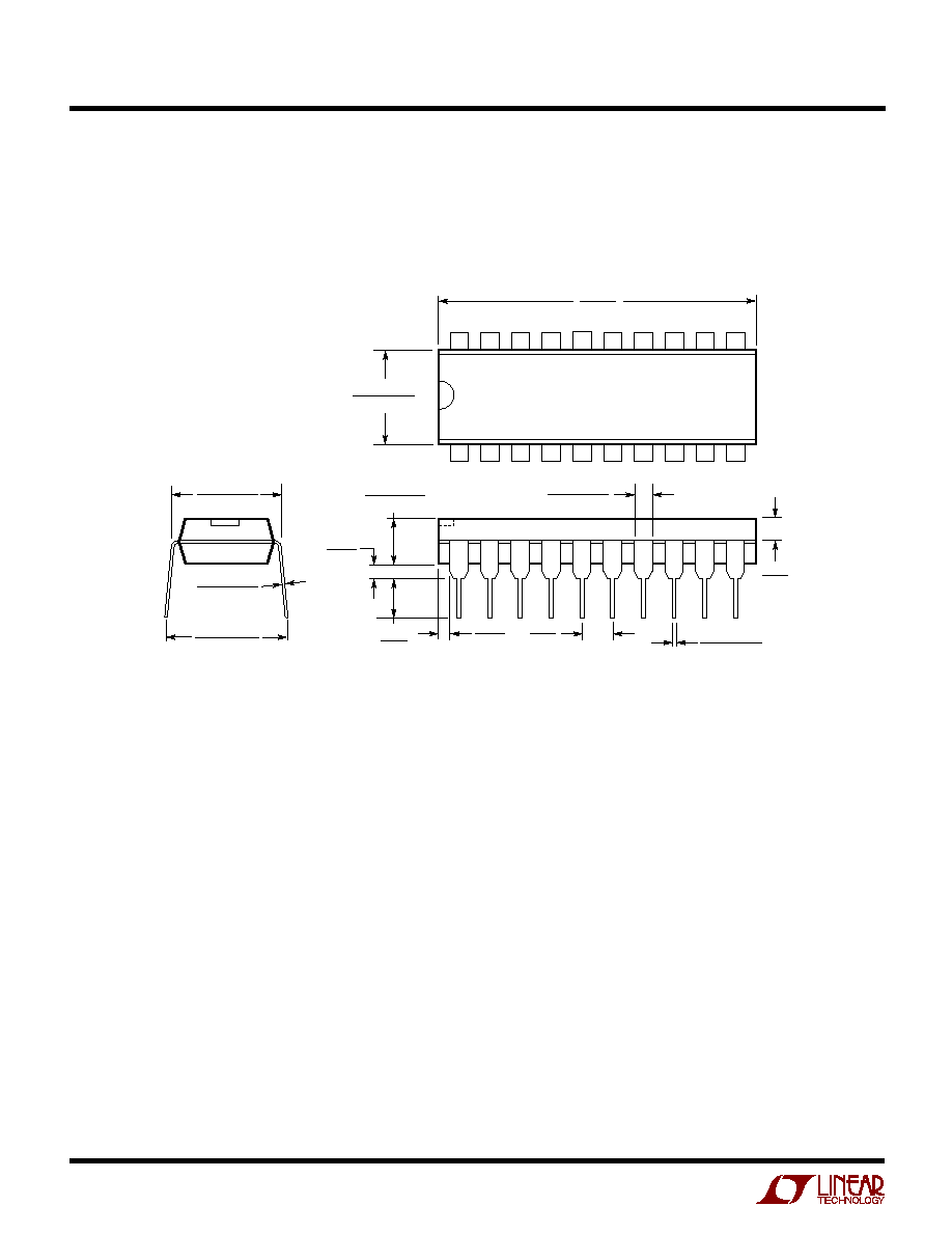
30
LTC1091/LTC1092
LTC1093/LTC1094
N Package
20-Lead PDIP (Narrow 0.300)
(LTC DWG # 05-08-1510)
N20 1098
0.020
(0.508)
MIN
0.125
(3.175)
MIN
0.130
±
0.005
(3.302
±
0.127)
0.065
(1.651)
TYP
0.045 ≠ 0.065
(1.143 ≠ 1.651)
0.018
±
0.003
(0.457
±
0.076)
0.005
(0.127)
MIN
0.100
(2.54)
BSC
0.255
±
0.015*
(6.477
±
0.381)
1.040*
(26.416)
MAX
1
2
3
4
5
6
7
8
9
10
19
11
12
13
14
16
15
17
18
20
0.009 ≠ 0.015
(0.229 ≠ 0.381)
0.300 ≠ 0.325
(7.620 ≠ 8.255)
0.325
+0.035
≠0.015
+0.889
≠0.381
8.255
(
)
*THESE DIMENSIONS DO NOT INCLUDE MOLD FLASH OR PROTRUSIONS.
MOLD FLASH OR PROTRUSIONS SHALL NOT EXCEED 0.010 INCH (0.254mm)
PACKAGE DESCRIPTIO
U
Dimensions in inches (millimeters) unless otherwise noted.
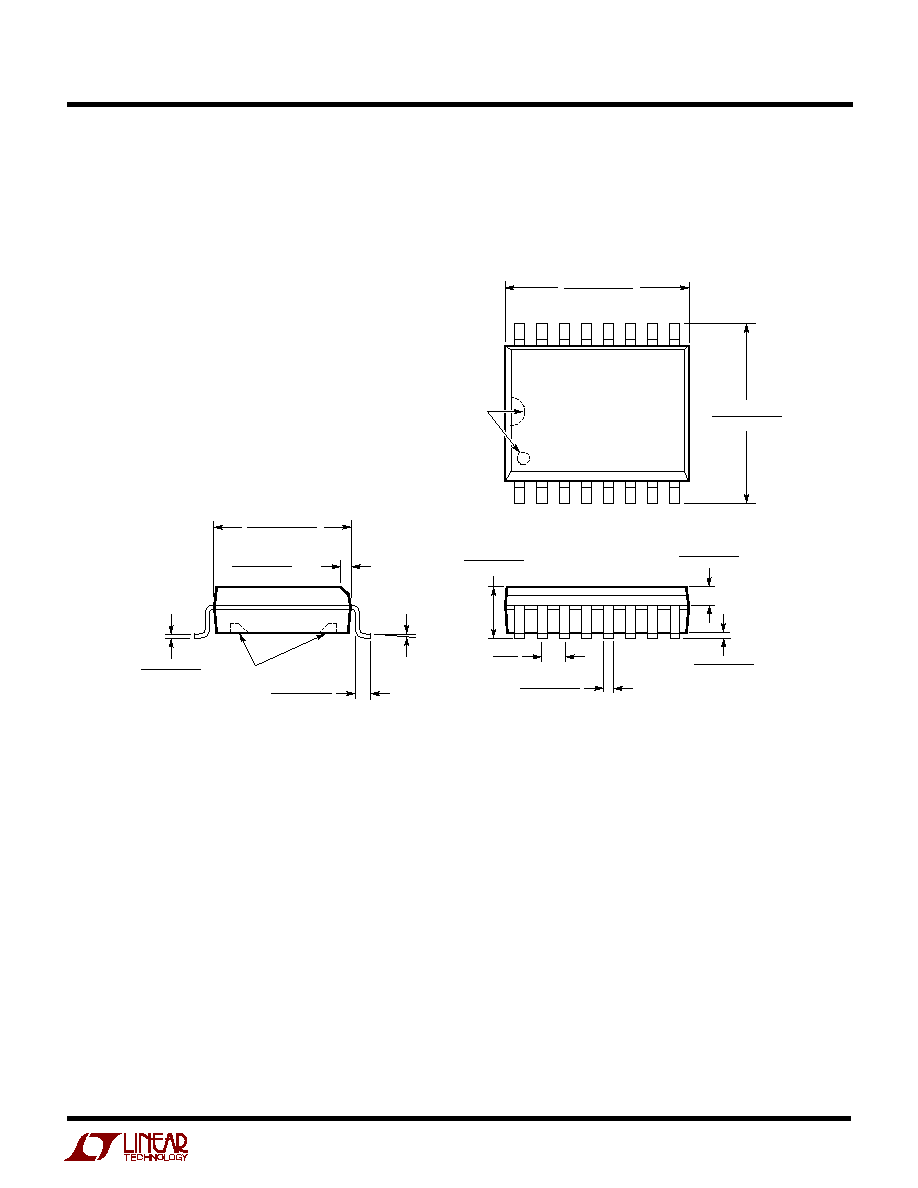
31
LTC1091/LTC1092
LTC1093/LTC1094
Information furnished by Linear Technology Corporation is believed to be accurate and reliable.
However, no responsibility is assumed for its use. Linear Technology Corporation makes no represen-
tation that the interconnection of circuits as described herein will not infringe on existing patent rights.
PACKAGE DESCRIPTIO
U
Dimensions in inches (millimeters) unless otherwise noted.
S16 (WIDE) 1098
NOTE 1
0.398 ≠ 0.413*
(10.109 ≠ 10.490)
16
15
14
13
12
11
10
9
1
2
3
4
5
6
7
8
0.394 ≠ 0.419
(10.007 ≠ 10.643)
0.037 ≠ 0.045
(0.940 ≠ 1.143)
0.004 ≠ 0.012
(0.102 ≠ 0.305)
0.093 ≠ 0.104
(2.362 ≠ 2.642)
0.050
(1.270)
BSC
0.014 ≠ 0.019
(0.356 ≠ 0.482)
TYP
0
∞
≠ 8
∞
TYP
NOTE 1
0.009 ≠ 0.013
(0.229 ≠ 0.330)
0.016 ≠ 0.050
(0.406 ≠ 1.270)
0.291 ≠ 0.299**
(7.391 ≠ 7.595)
◊
45
∞
0.010 ≠ 0.029
(0.254 ≠ 0.737)
NOTE:
1. PIN 1 IDENT, NOTCH ON TOP AND CAVITIES ON THE BOTTOM OF PACKAGES ARE THE MANUFACTURING OPTIONS.
THE PART MAY BE SUPPLIED WITH OR WITHOUT ANY OF THE OPTIONS
DIMENSION DOES NOT INCLUDE MOLD FLASH. MOLD FLASH SHALL NOT EXCEED 0.006" (0.152mm) PER SIDE
DIMENSION DOES NOT INCLUDE INTERLEAD FLASH. INTERLEAD FLASH SHALL NOT EXCEED 0.010" (0.254mm) PER SIDE
*
**
SW Package
16-Lead Plastic Small Outline (Wide 0.300)
(LTC DWG # 05-08-1620)
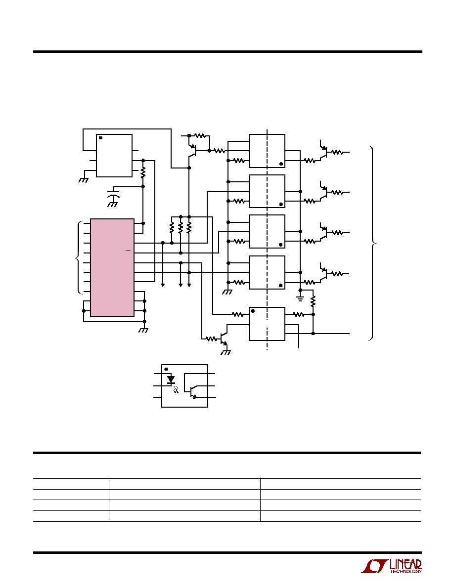
32
LTC1091/LTC1092
LTC1093/LTC1094
1091fa LT/TP 1099 2K REV A ∑ PRINTED IN USA
©
LINEAR TECHNOLOGY CORPORATION 1988
Linear Technology Corporation
1630 McCarthy Blvd., Milpitas, CA 95035-7417
(408) 432-1900
q
FAX: (408) 434-0507
q
www.linear-tech.com
PART NUMBER
DESCRIPTION
COMMENTS
LTC1090
10-Bit, 8-Channel ADC
Serial I/O, 1.5mA Supply Current
LTC1291/LTC1292
12-BIT, 2-Channel and Differential ADCs
Pin Compatible Upgrades to LTC1091/LTC1092
LTC1293/LTC1294
12-Bit, 6- and 8-Channel ADCs
Pin Compatible Upgrades to LTC1093/LTC1094
RELATED PARTS
LT1021-5
5V
MISO
MOSI
C0
SCK
C1
10k
10k
9V
ISOLATION
BARRIER
4N28s
51k
51k
51k
51k
300
5.1k
◊
3
5V
5V
5V
5V
51k
5.1k
10k
10k
10k
10k
150
150
150
150
4N28
TO ADDITIONAL
LTC1094s
NC
4N28
*SOLID TANTALUM
**MC68HC05 CODE AVAILABLE FROM
LINEAR TECHNOLOGY
10
µ
F*
1
8 ANALOG
INPUTS
0V TO 5V
RANGE
TO
68HC05**
10k
LT1091-4 TA06
CH0
CH1
CH2
CH3
CH4
CH5
CH6
CH7
COM
DGND
DV
CC
AV
CC
CLK
CS
D
OUT
D
IN
REF
+
REF
≠
AGND
V
≠
LTC1094
2N3906
2N3904
2N3906
+
TYPICAL APPLICATIO
N
U
Micropower, 500V Optoisolated, Multichannel, 10-Bit Data
Acquisition System Is Accessed Once Every Two Seconds