 | –≠–ª–µ–∫—Ç—Ä–æ–Ω–Ω—ã–π –∫–æ–º–ø–æ–Ω–µ–Ω—Ç: LTC1096L | –°–∫–∞—á–∞—Ç—å:  PDF PDF  ZIP ZIP |
1
LTC1096L/LTC1098L
Low Voltage, Micropower
Sampling 8-Bit Serial I/O
A/D Converters
December 1995
Information furnished by Linear Technology Corporation is believed to be accurate and reliable.
However, no responsibility is assumed for its use. Linear Technology Corporation makes no represen-
tation that the interconnection of its circuits as described herein will not infringe on existing patent rights.
Final Electrical Specifications
D
U
ESCRIPTIO
S
FEATURE
s
Specified at 2.65V Minimum Supply
s
Maximum Supply Current: 80
µ
A
s
Auto Shutdown to 1nA
s
8-Pin SO Package
s
On-Chip Sample-and-Hold
s
Conversion Time: 32
µ
s
s
Sample Rates: 16.5ksps
s
I/O Compatible with SPI, MICROWIRE
TM
, etc.
The LTC
Æ
1096L/LTC1098L are 3V micropower, 8-bit suc-
cessive approximation sampling A/D converters. They
typically draw only 40
µ
A of supply current when convert-
ing and automatically power down to a typical supply
current of 1nA between conversions. They are packaged in
8-pin SO packages and operate on a 3V supply. These 8-
bit, switched capacitor, successive approximation ADCs
include a sample-and-hold. The LTC1096L has a single
differential analog input. The LTC1098L offers a software
selectable 2-channel multiplexed input.
On-chip serial ports allow efficient data transfer to a wide
range of microprocessors and microcontrollers over three
wires. This, coupled with micropower consumption, makes
remote location possible and facilitates transmitting data
through isolation barriers.
The circuits can be used in ratiometric applications or with
an external reference. The high impedance analog inputs
and the ability to operate with reduced spans (to 1V full
scale) allow direct connection to sensors and transducers
in many applications, eliminating the need for gain stages.
s
Battery-Operated Systems
s
Remote Data Acquisition
s
Isolated Data Acquisition
s
Battery Monitoring
s
Temperature Measurement
U
S
A
O
PPLICATI
, LTC and LT are registered trademarks of Linear Technology Corporation.
MICROWIRE is a registered trademark of National Semiconductor Corporation.
U
A
O
PPLICATI
TYPICAL
SAMPLE FREQUENCY (kHz)
0.1
1
SUPPLY CURRENT, I
CC
(
µ
A)
10
100
1000
1
10
100
1096/8 TA02
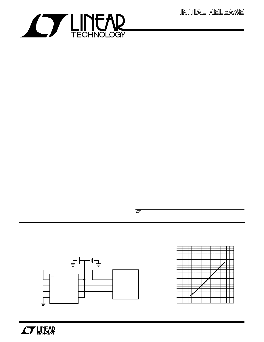
Supply Current vs Sample Rate
10
µ
W, SO-8 Package, 8-Bit A/D Converter
Samples at 200Hz and Runs Off a 3V Battery
3V
1
µ
F
ANALOG INPUT
V
CC
CLK
D
OUT
V
REF
8
7
6
5
1
2
3
4
LTC1096L
MPU
SERIAL DATA LINK
(MICROWIRE AND
SPI COMPATIBLE)
SERIAL DATA LINK
0V TO 3V RANGE
1096/8 TA01
CS/
SHDN
+IN
≠IN
GND

2
LTC1096L/LTC1098L
A
U
G
W
A
W
U
W
A
R
BSOLUTE
XI
TI
S
Operating Temperature
LTC1096LAC/LTC1098LAC .................... 0
∞
C to 70
∞
C
LTC1096LAI/LTC1098LAI .................. ≠ 40
∞
C to 85
∞
C
LTC1096LC/LTC1098LC ......................... 0
∞
C to 70
∞
C
LTC1096LI/LTC1098LI ....................... ≠ 40
∞
C to 85
∞
C
Storage Temperature Range ................. ≠ 65
∞
c to 150
∞
C
Lead Temperature (Soldering, 10 sec.)................ 300
∞
C
Supply Voltage (V
CC
) to GND ................................... 12V
Voltage
Analog and Reference ................ ≠0.3V to V
CC
+ 0.3V
Digital Inputs ......................................... ≠0.3V to 12V
Digital Outputs ........................... ≠0.3V to V
CC
+ 0.3V
Power Dissipation .............................................. 500mW
(Notes 1 and 2)
W
U
U
PACKAGE/ORDER I FOR ATIO
(Note 3)
ORDER PART
NUMBER
ORDER PART
NUMBER
LTC1098LACS8
LTC1098LAIS8
LTC1098LCS8
LTC1098LIS8
LTC1096LACS8
LTC1096LAIS8
LTC1096LCS8
LTC1096LIS8
SYMBOL
PARAMETER
CONDITIONS
MIN
TYP
MAX
UNITS
V
CC
Supply Voltage
2.65
4.0
V
f
CLK
Clock Frequency
V
CC
= 2.65V
25
250
kHz
t
CYC
Total Cycle Time
LTC1096L, f
CLK
= 250kHz
58
µ
s
LTC1098L, f
CLK
= 250kHz
58
µ
s
t
hDI
Hold Time, D
IN
After CLK
V
CC
= 2.65V
450
ns
t
suCS
Setup Time CS
Before First CLK
(See Operating Sequence)
V
CC
= 2.65V, LTC1096L
1
µ
s
V
CC
= 2.65V, LTC1098L
1
µ
s
t
WAKEUP
Wakeup Time CS
Before First CLK
After First CLK
V
CC
= 2.65V, LTC1096L
10
µ
s
(See Figure 1, LTC1096L Operating Sequence)
Wakeup Time CS
Before MSBF Bit CLK
V
CC
= 2.65V, LTC1098L
10
µ
s
(See Figure 2, LTC1098L Operating Sequence)
t
suDI
Setup Time, D
IN
Stable Before CLK
V
CC
= 2.65V
1
µ
s
t
WHCLK
CLK High Time
V
CC
= 2.65V
1.6
µ
s
t
WLCLK
CLK Low Time
V
CC
= 2.65V
1.6
µ
s
t
WHCS
CS High Time Between Data Transfer Cycles
V
CC
= 2.65V
2
µ
s
t
WLCS
CS Low Time During Data Transfer
LTC1096L, f
CLK
= 250kHz
56
µ
s
LTC1098L, f
CLK
= 250kHz
56
µ
s
RECO E DED OPERATI G CO DITIO S
W
U
W
U
U
U
Consult factory for Military grade parts.
098LIA
1098LA
1098LI
1098L
096LIA
1096LA
1096LI
1096L
S8 PART MARKING
S8 PART MARKING
TOP VIEW
+IN
≠IN
GND
V
CC
CLK
D
OUT
V
REF
S8 PACKAGE
8-LEAD PLASTIC SO
CS/
SHDN
1
2
3
4
8
7
6
5
TOP VIEW
CH0
CH1
GND
V
CC
(V
REF)
CLK
D
OUT
D
IN
S8 PACKAGE
8-LEAD PLASTIC SO
CS/
SHDN
1
2
3
4
8
7
6
5
T
JMAX
= 150
∞
C,
JA
= 175
∞
C/W
T
JMAX
= 150
∞
C,
JA
= 175
∞
C/W

3
LTC1096L/LTC1098L
PARAMETER
CONDITIONS
MIN
TYP
MAX
MIN
TYP
MAX
UNITS
Resolution (No Missing Code)
q
8
8
Bits
Offset Error
(Note 4)
q
±
0.5
±
1
LSB
Linearity Error
q
±
0.5
±
1
LSB
Full Scale Error
q
±
0.5
±
1
LSB
Total Unadjusted Error (Note 5)
V
REF
= 2.5V
q
±
1
±
1.5
LSB
Analog Input Range
(Note 6)
V
REF Input Range (Note 6)
2.65
V
CC
4.0V
V
Analog Input Leakage Current
(Note 7)
q
±
1
±
1
µ
A
CO VERTER A D ULTIPLEXER CHARACTERISTICS
U
U W
V
CC
= 2.65V, V
REF
= 2.5V, f
CLK
= 250kHz, unless otherwise noted.
LTC1096L/LTC1098L
LTC1096LA/LTC1098LA
≠ 0.05V to V
CC
+ 0.05V
≠ 0.05V to V
CC
+ 0.05V
SYMBOL
PARAMETER
CONDITIONS
MIN
TYP
MAX
UNITS
V
IH
High Level Input Voltage
V
CC
= 3.6V
q
1.9
V
V
IL
Low Level Input Voltage
V
CC
= 2.65V
q
0.45
V
I
IH
High Level Input Current
V
IN
= V
CC
q
2.5
µ
A
I
IL
Low Level Input Current
V
IN
= 0V
q
≠ 2.5
µ
A
V
OH
High Level Output Voltage
V
CC
= 2.65V, I
O
= 10
µ
A
q
2.4
2.64
V
I
O
= 360
µ
A
q
2.1
2.50
V
V
OL
Low Level Output Voltage
V
CC
= 2.65V, I
O
= 400
µ
A
q
0.3
V
I
OZ
Hi-Z Output Leakage
CS =High
q
±
3
µ
A
I
SOURCE
Output Source Current
V
OUT
= 0V
≠ 10
mA
I
SINK
Output Sink Current
V
OUT
= V
CC
15
mA
I
REF
Reference Current
CS = V
CC
q
0.001
2.5
µ
A
t
CYC
200
µ
s, f
CLK
50kHz
q
3.500
7.5
µ
A
t
CYC
= 58
µ
s, f
CLK
= 250kHz
q
35.00
50.0
µ
A
I
CC
Supply Current
CS = V
CC
q
0.001
±
3
µ
A
LTC1096L,
t
CYC
200
µ
s, f
CLK
50kHz
q
40
80
µ
A
t
CYC
= 58
µ
s, f
CLK
= 250kHz
q
120
180
µ
A
LTC1098L,
t
CYC
200
µ
s, f
CLK
50kHz
q
44
88
µ
A
t
CYC
= 58
µ
s, f
CLK
= 250kHz
q
155
230
µ
A
V
CC
= 2.65V, V
REF
= 2.5V, f
CLK
= 250kHz, unless otherwise noted.
ELECTRICAL C
C
HARA TER STICS
DIGITAL A D
U
I
DC
4
LTC1096L/LTC1098L
AC CHARACTERISTICS
V
CC
= 2.65V, V
REF
= 2.5V, f
CLK
= 250kHz, unless otherwise noted.
SYMBOL
PARAMETER
CONDITIONS
MIN
TYP
MAX
UNITS
t
SMPL
Analog Input Sample Time
See Operating Sequences
1.5
CLK Cycles
f
SMPL(MAX)
Maximum Sampling Frequency
q
16.5
kHz
t
CONV
Conversion Time
See Operating Sequences
8
CLK Cycles
t
dDO
Delay Time, CLK
to D
OUT
Data Valid
See Test Circuits
q
500
1000
ns
t
dis
Delay Time, CS
to D
OUT
Hi-Z
See Test Circuits
q
220
800
ns
t
en
Delay Time, CLK
to D
OUT
Enable
See Test Circuits
q
160
480
ns
t
hDO
Time Output Data Remains Valid After CLK
C
LOAD
= 100pF
400
ns
t
f
D
OUT
Fall Time
See Test Circuits
q
70
250
ns
t
r
D
OUT
Rise Time
See Test Circuits
q
50
200
ns
C
IN
Input Capacitance
Analog Inputs On Channel
25
pF
Off Channel
5
pF
Digital Input
5
pF
LTC1096L
CS/SHDN (Pin 1): Chip Select Input. A logic low on this
input enables the LTC1096L. A logic high on this input
disables the LTC1096L and disconnects the power to the
LTC1096L.
IN
+
(Pin 2): Analog Input. This input must be free of noise
with respect to GND.
IN
≠
(Pin 3): Analog Input. This input must be free of noise
with respect to GND.
GND (Pin 4): Analog Ground. GND should be tied directly
to an analog ground plane.
V
REF
(Pin 5): Reference Input. The reference input defines
the span of the A/D converter and must be kept free of
noise with respect to GND.
D
OUT
(Pin 6): Digital Data Output. The A/D conversion
result is shifted out of this output.
CLK (Pin 7): Shift Clock. This clock synchronizes the serial
data transfer.
V
CC
(Pin 8): Power Supply Voltage. This pin provides
power to the A/D converter. It must be free of noise and
ripple by bypassing directly to the analog ground plane.
LTC1098L
CS/SHDN (Pin 1): Chip Select Input. A logic low on this
input enables the LTC1098L. A logic high on this input
disables the LTC1098L and disconnects the power to the
LTC1098L.
CHO (Pin 2): Analog Input. This input must be free of noise
with respect to GND.
The
q
denotes specifications which apply over the full operating
temperature range.
Note 1: Absolute Maximum Ratings are those values beyond which the life
of a device may be impaired.
Note 2: All voltage values are with respect to GND.
Note 3: This device is specified at 2.65V. Consult factory for 5V specified
devices.
Note 4: Linearity error is specified between the actual end points of the
A/D transfer curve.
Note 5: Total unadjusted error includes offset, full scale, linearity,
multiplexer and hold step errors.
Note 6: Two on-chip diodes are tied to each reference and analog input
which will conduct for reference or analog input voltages one diode drop
below GND or one diode drop above V
CC
. This spec allows 50mV forward
bias of either diode for 2.65V
V
CC
3.6V. This means that as long as the
reference or analog input does not exceed the supply voltage by more than
50mV, the output code will be correct. To achieve an absolute 0V to 3V
input voltage range will therefore require a minimum supply voltage of
2.950V over initial tolerance, temperature variations and loading.
Note 7: Channel leakage current is measured after the channel selection.
PI FU CTIO S
U
U
U
5
LTC1096L/LTC1098L
PI FU CTIO S
U
U
U
CH1 (Pin 3): Analog Input. This input must be free of noise
with respect to GND.
GND (Pin 4): Analog Ground. GND should be tied directly
to an analog ground plane.
D
IN
(Pin 5): Digital Data Input. The multiplexer address is
shifted into this pin.
D
OUT
(Pin 6): Digital Data Output. The A/D conversion
result is shifted out of this output.
CLK (Pin 7): Shift Clock. This clock synchronizes the serial
data transfer.
V
CC
(V
REF
)
(Pin 8): Power Supply Voltage. This pin pro-
vides power and defines the span of the A/D converter. It
must be free of noise and ripple by bypassing directly to
the analog ground plane
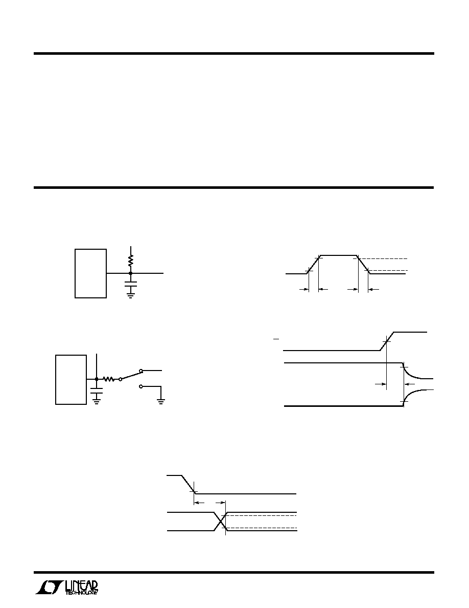
TEST CIRCUITS
Load Circuit for t
dDO
, t
r
and t
f
Voltage Waveforms for D
OUT
Rise and Fall Times, t
r
, t
f
D
OUT
1.4V
3k
100pF
TEST POINT
LTC1096/98 ∑ TC01
D
OUT
t
r
t
f
LTC1096/98 ∑ TC02
V
OH
V
OL
Load Circuit for t
dis
and t
en
Voltage Waveforms for t
dis
D
OUT
WAVEFORM 1
(SEE NOTE 1)
V
IH
t
dis
90%
10%
D
OUT
WAVEFORM 2
(SEE NOTE 2)
CS
NOTE 1: WAVEFORM 1 IS FOR AN OUTPUT WITH INTERNAL CONDITIONS SUCH
THAT THE OUTPUT IS HIGH UNLESS DISABLED BY THE OUTPUT CONTROL.
NOTE 2: WAVEFORM 2 IS FOR AN OUTPUT WITH INTERNAL CONDITIONS SUCH
THAT THE OUTPUT IS LOW UNLESS DISABLED BY THE OUTPUT CONTROL.
LTC1096/98 ∑ TC04
D
OUT
3k
100pF
TEST POINT
V
CC
t
dis
WAVEFORM 2, t
en
t
dis
WAVEFORM 1
LTC1096/98 ∑ TC03
Voltage Waveforms for D
OUT
Delay Time, t
dDO
CLK
D
OUT
V
IL
t
dDO
V
OH
V
OL
LTC1096/98 ∑ TC05