 | ÐлекÑÑоннÑй компоненÑ: LTC1100 | СкаÑаÑÑ:  PDF PDF  ZIP ZIP |
Äîêóìåíòàöèÿ è îïèñàíèÿ www.docs.chipfind.ru
LTC1100
1
D
U
ESCRIPTIO
S
FEATURE
The LTC1100 is a high precision instrumentation ampli-
fier using chopper-stabilization techniques to achieve
outstanding DC performance. The input DC offset is
typically 1
µ
V while the DC offset drift is typically 10nV/
°
C;
a very low bias current of 50pA is also achieved.
The LTC1100 is self-contained; that is, it achieves a differ-
ential gain of 100 without any external gain setting resistor
or trim pot. The gain linearity is 8ppm and the gain drift is
4ppm/
°
C. The LTC1100 operates from a single 5V supply
up to
±
8V. The output typically swings 300mV from its
power supply rails with a 10k load.
An optional external capacitor can be added from pin 7 to
pin 8 to tailor the device's 18kHz bandwidth and to
eliminate any unwanted noise pickup.
The LTC1100 is also offered in a 16-pin surface mount
package with selectable gains of 10 or 100.
The LTC1100 is manufactured using Linear Technology's
enhanced LTCMOS
TM
silicon gate process.
Precision, Chopper-Stabilized
Instrumentation Amplifier
s
Offset Voltage: 10
µ
V Max
s
Offset Voltage Drift: 50nV/
°
C Max
s
Bias Current: 50pA Max
s
Offset Current: 50pA Max
s
Gain Nonlinearity: 8ppm Max
s
Gain Error:
±
0.05% Max
s
CMRR: 104dB
s
0.1Hz to 10Hz Noise: 2
µ
V
P-P
s
Single 5V Supply Operation
s
8-Pin MiniDIP
U
S
A
O
PPLICATI
s
Thermocouple Amplifiers
s
Strain Gauge Amplifiers
s
Differential to Single-Ended Converters
LTCMOS is a trademark of Linear Technology Corporation
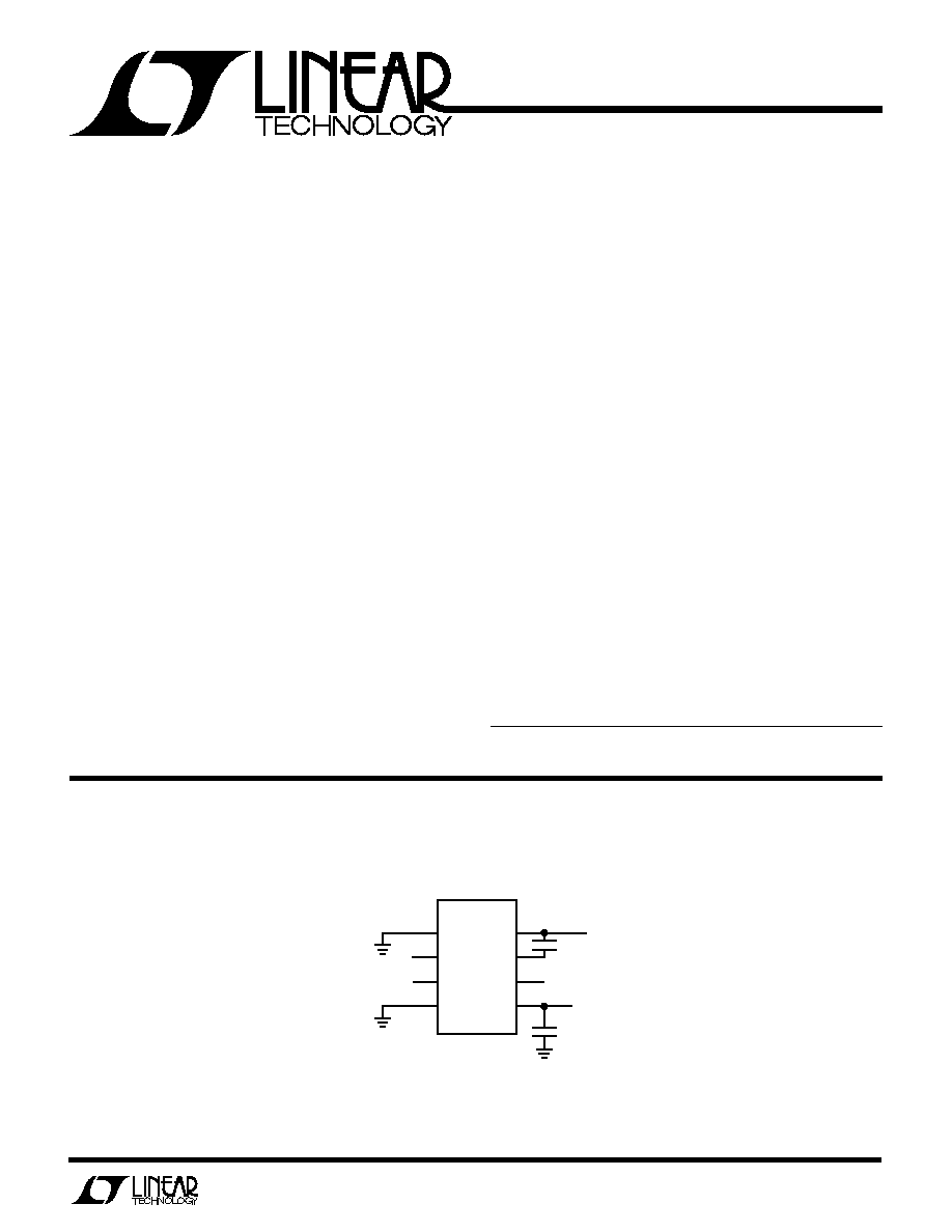
Single 5V Supply, DC Instrumentation Amplifier
V
IN
0.1
µ
F
0.01
µ
F
1
2
3
4
8
7
6
5
V
OUT
V
IN
V
+
= 5V
V
OUT
= 100 [V
IN
(V
IN
)]
LTC1100
LTC1100 · TA01
U
A
O
PPLICATI
TYPICAL
LTC1100
2
A
U
G
W
A
W
U
W
A
R
BSOLUTE
XI
TI
S
W
U
U
PACKAGE/ORDER I FOR ATIO
ORDER PART
NUMBER
LTC1100ACS
LTC1100CS
ORDER PART
NUMBER
1
2
3
4
5
6
7
8
TOP VIEW
S PACKAGE
16-LEAD PLASTIC SOL
16
15
14
13
12
11
10
9
NC
GND REF
G = 10
CMRR
NC
V
IN
V
NC
NC
V
OUT
G = 10
COMP
NC
V
IN
V
+
NC
1
2
3
4
8
7
6
5
TOP VIEW
GND REF
CMRR
V
IN
V
V
OUT
COMP
V
IN
V
+
N8 PACKAGE
8-LEAD PLASTIC DIP
J8 PACKAGE
8-LEAD CERAMIC DIP
T
JMAX
= 150
°
C,
JA
= 100
°
C/W (J)
T
JMAX
= 110
°
C,
JA
= 130
°
C/W (N)
ELECTRICAL C
C
HARA TERISTICS
V
S
=
±
5V, R
L
= 10k, C
C
= 1000pF, unless otherwise specified.
LTC1100ACN (Note 3)
LTC1100CN/CJ
PARAMETER
CONDITIONS
MIN
TYP
MAX
MIN
TYP
MAX
UNITS
Gain Error
T
A
= 25
°
C
0.01
0.05
0.01
0.075
±
%
q
0.10
0.150
±
%
Gain Nonlinearity
T
A
= 25
°
C
3
8
3
20
ppm
q
12
30
12
60
ppm
Input Offset Voltage
(Note 1)
±
1
±
10
±
1
±
10
µ
V
Input Offset Voltage Drift
(Note 1)
q
±
5
±
100
±
5
±
100
nV/
°
C
Input Noise Voltage
DC to 10Hz, T
A
= 25
°
C
1.9
1.9
µ
V
P-P
Input Bias Current
T
A
= 25
°
C
2.5
50
2.5
65
pA
q
120
135
pA
Input Offset Current
q
10
50
10
65
pA
Common-Mode Rejection Ratio
V
CM
= 2.3V to
-
4.7V (Note 2)
q
104
115
90
110
dB
Power Supply Rejection Ratio
V
S
=
±
2.375V to
±
8V
q
120
105
dB
Output Voltage Swing
R
L
= 2k, V
S
=
±
8V
q
7.2
6.2
7.2
6.2
V
R
L
=10k, V
S
=
±
8V
q
7.7
7.5
7.7
7.5
V
Supply Current
T
A
= 25
°
C
2.4
2.8
2.4
3.3
mA
q
3.4
4.0
3.4
4.5
mA
Internal Sampling Frequency
T
A
= 25
°
C
2.8
2.8
kHz
Bandwidth
T
A
= 25
°
C
18
18
kHz
Contact factory for Industrial grade parts
Operating Temperature Range
LTC1100M/AM ................................
-
55
°
C to 125
°
C
LTC1100C/AC ....................................
-
40
°
C to 85
°
C
Output Short Circuit Duration ......................... Indefinite
Storage Temperature Range ................
-
65
°
C to 150
°
C
Total Supply Voltage (V
+
to V
-
) ............................. 18V
Input Voltage ....................... (V
+
+
0.3V) to (V
-
-
0.3V)
Lead Temperature (Soldering, 10 sec) ................. 300
°
C
T
JMAX
= 110
°
C,
JA
= 100
°
C/W
LTC1100ACN8
LTC1100CJ8
LTC1100CN8
LTC1100AMJ8
LTC1100MJ8
LTC1100
3
LTC1100AMJ (Note 3)
LTC1100MJ
PARAMETER
CONDITIONS
MIN
TYP
MAX
MIN
TYP
MAX
UNITS
Gain Error
T
A
= 25
°
C
0.01
0.05
0.01
0.075
±
%
q
0.11
0.150
±
%
Gain Nonlinearity
T
A
= 25
°
C
3
8
3
20
ppm
q
40
65
ppm
Input Offset Voltage
(Note 1)
±
1
±
10
±
1
±
10
µ
V
Input Offset Voltage Drift
(Note 1)
q
±
5
±
100
±
5
±
100
nV/
°
C
Input Noise Voltage
DC to 10Hz, T
A
= 25
°
C
1.9
1.9
µ
V
P-P
Input Bias Current
T
A
= 25
°
C
5
50
5
65
pA
q
300
450
pA
Input Offset Current
q
80
120
pA
Common-Mode Rejection Ratio
V
CM
=
-
4.7V to 2.3V
q
100
90
dB
Power Supply Rejection Ratio
V
S
=
±
2.375V to
±
8V
q
115
95
dB
Output Voltage Swing
R
L
= 10k, V
S
=
±
8V
q
7.4
7.4
7.4
7.4
V
R
L
= 2k, V
S
=
±
8V
q
7.0
6.0
7.0
6.0
V
Supply Current
T
A
= 25
°
C
2.4
2.4
3.3
mA
q
4.2
4.6
mA
Internal Sampling Frequency
T
A
= 25
°
C
2.8
2.8
kHz
Bandwidth
T
A
= 25
°
C
18
18
kHz
ELECTRICAL C
C
HARA TERISTICS
V
S
=
±
5V, R
L
= 10k, C
C
= 1000pF, unless otherwise specified.
ELECTRICAL C
C
HARA TERISTICS
LTC1100ACS (Note 3)
LTC1100CS
PARAMETER
CONDITIONS
MIN
TYP
MAX
MIN
TYP
MAX
UNITS
Gain Error
T
A
= 25
°
C, A
V
=100
0.01
0.05
0.01
0.075
±
%
A
V
=100
q
0.10
0.150
±
%
A
V
=10
0.01
0.04
0.01
0.060
±
%
A
V
=10
q
0.10
0.150
±
%
Gain Nonlinearity
T
A
= 25
°
C, A
V
=100
3
8
3
20
ppm
A
V
=100
q
12
30
12
60
ppm
A
V
=10
1
8
1
10
ppm
A
V
=10
q
25
40
ppm
Input Offset Voltage
(Note 1)
±
1
±
10
±
1
±
10
µ
V
Input Offset Voltage Drift
(Note 1)
q
±
5
±
100
±
5
±
100
nV/
°
C
Input Noise Voltage
DC to 10Hz, T
A
= 25
°
C
1.9
1.9
µ
V
P-P
Input Bias Current
T
A
= 25
°
C
2.5
50
2.5
65
pA
q
120
135
pA
Input Offset Current
q
10
50
10
65
pA
Common-Mode Rejection Ratio
V
CM
=
-
4.7V to 2.3V,
A
V
=100
q
104
115
90
110
dB
A
V
=10
q
95
85
dB
Power Supply Rejection Ratio
V
S
=
±
2.375V to
±
8V
q
120
105
dB
V
S
=
±
5V, R
L
= 10k, C
C
= 1000pF, unless otherwise specified.
LTC1100
4
ELECTRICAL C
C
HARA TERISTICS
V
S
=
±
5V, R
L
= 10k, C
C
= 1000pF, unless otherwise specified.
LTC1100ACS (Note 3)
LTC1100CS
PARAMETER
CONDITIONS
MIN
TYP
MAX
MIN
TYP
MAX
UNITS
Output Voltage Swing
R
L
=10k, V
S
=
±
8V
q
7.2
6.2
7.2
6.2
V
R
L
= 2k, V
S
=
±
8V
q
7.7
7.5
7.7
7.5
V
Supply Current
T
A
= 25
°
C
2.4
2.8
2.4
3.3
mA
q
3.4
4.0
3.4
4.5
mA
Internal Sampling Frequency
T
A
= 25
°
C
2.8
2.8
kHz
Bandwidth G = 100
T
A
= 25
°
C
18
18
kHz
G = 10
180
180
kHz
The
q
denotes the specifications which apply over the full operating
temperature range.
Note 1: These parameters are guaranteed by design. Thermocouple effects
preclude measurement of these voltage levels in high speed automatic test
systems. V
OS
is measured to a limit determined by test equipment
capability.
Note 2: See Applications Information, Single Supply Operation.
Note 3: Please consult Linear Technology Marketing.
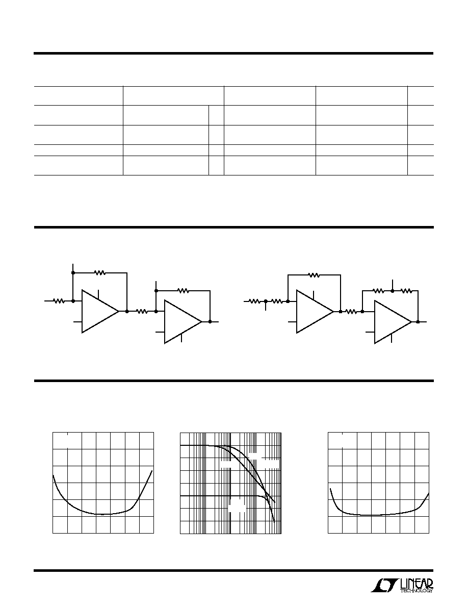
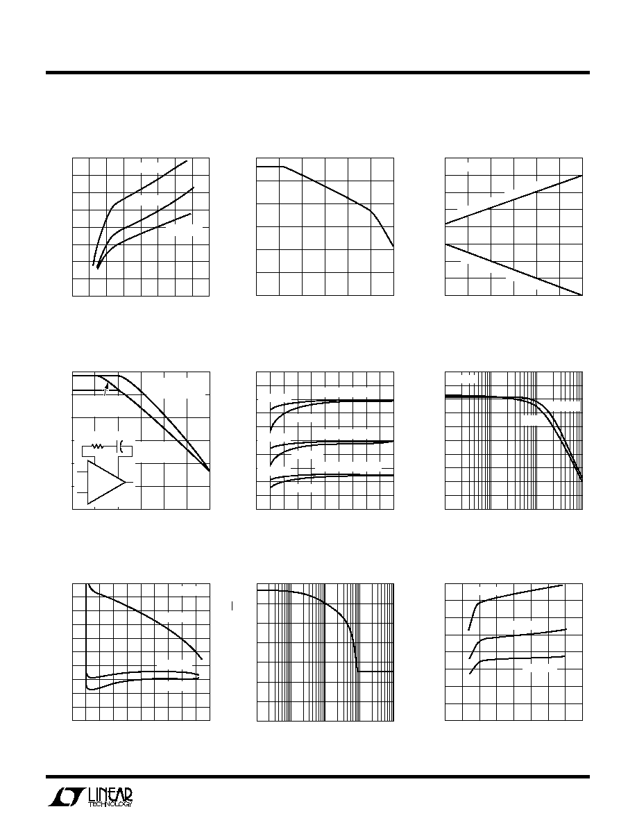
BLOCK DIAGRA S
W
C
C
HARA TERISTICS
U
W
A
TYPICAL PERFOR
CE
Gain Error vs Temperature
FREQUENCY (Hz)
15
DIFFERENTIAL GAIN (dB)
20
25
30
35
100
10k
100k
1M
LTC1100 · TPC02
1k
40
30
60
90
120
150
180
(G = 100)
GAIN
PHASE
PHASE SHIFT (DEGREES)
45
10
5
0
30
210
GAIN
(G = 10)
Gain, Phase vs Frequency
Gain Nonlinearity
vs Temperature
LTC1100 · BD01
4 (V
)
6
R
99R
8
7
5 (V
+
)
R
2
3
99R
1
+
+
R = 2.5k
10 (V )
+
LTC1100 · BD02
7 (V )
11
R
90R
15
14
R
6
9R
-
+
+
9R
13
4
2
90R
3
R = 2.5k
NOTE: FOR A VOLTAGE GAIN OF 10V/V SHORT PIN 2 TO 3, AND PIN 14 TO 15.
TEMPERATURE (°C)
50
GAIN ERROR (±
%)
0
0.01
0.02
0.03
25
0
25
50
LTC1100 · TPC01
75
100
125
0.04
0.05
0.01
V
S
= ±8V
R
L
= 50k
TEMPERATURE (°C)
50
GAIN NONLINEARITY (ppm)
0
5
10
15
25
0
25
50
LTC1100 · TPC03
75
100
125
20
25
5
V
S
= ±8V
R
L
= 50k
LTC1100
5
C
C
HARA TERISTICS
U
W
A
TYPICAL PERFOR
CE
Power Supply Rejection Ratio
Common-Mode Range
Supply Current vs Supply Voltage
vs Frequency
vs Supply Voltage
Undistorted Output Swing
CMRR vs Frequency
Output Voltage Swing vs Load
vs Frequency
Bias Current vs
Internal Sampling Frequency
Common-Mode Voltage
Voltage Noise vs Frequency
vs Supply Voltage
LOAD RESISTANCE (k
)
0
V
OUT
± SWING (V)
0
±1
±2
±3
1
2
3
4
LTC1100 · TPC08
5
6
7
±4
±5
8
9
10
±6
±7
±8
NEGATIVE
POSITIVE
NEGATIVE
POSITIVE
POSITIVE
NEGATIVE
±9
±10
V
S
= ±8V, T
A
85°C
V
S
= ±5V, T
A
85°C
V
S
= ±2.5V, T
A
85°C
FREQUENCY (Hz)
0.1
20
0
CMRR (dB)
60
40
100
80
120
1
10
100
1k
LTC1100 · TPC07
10k
100k
+
3
6
1
2
R
C
C
C
LTC1100
G = 100, R
C
= 100k
C
C
= 10pF
G = 10, R
C
=
C
C
= 0pF
G = 100, R
C
=
C
C
= 0pF
FREQUENCY (Hz)
100
0
PEAK-TO-PEAK OUTPUT SWING (V)
1
3
4
10
1k
10k
100k
LTC1100 · TPC09
2
5
6
7
8
9
R
L
= 100k
R
L
= 2k
V
S
= ±5V
COMMON-MODE VOLTAGE (V)
BIAS CURRENT (pA)
300
180
120
60
5 4 3 2
LTC1100 · TPC10
1
0
1
0
60
2
3
4
120
180
240
V
S
= ±5V
T
A
= 25°C
T
A
= 125°C
T
A
= 55°C
6
200
360
2
4
SAMPLING FREQUENCY (kHz)
1
2
6
10
14
LTC1100 · TPC12
4
8
12
16
3
T
A
= 25°C
T
A
= 55°C
T
A
= 125°C
18
0
TOTAL SUPPLY VOLTAGE V
+
TO V
(V)
FREQUENCY (Hz)
0.1
POWER SUPPLY REJECTION RATIO (dB)
25
50
75
100
1
10
100
LTC1100 · TPC05
1k
10k
100k
125
150
0
TOTAL SUPPLY VOLTAGE V
+
TO V
(V)
2
0
SUPPLY CURRENT (mA)
1
2
6
10
14
LTC1100 · TPC04
4
8
12
16
3
4
T
A
= 55°C
T
A
= 25°C
T
A
= 125°C
18
SUPPLY VOLTAGE (V)
8
COMMON-MODE RANGE (V)
6
4
2
0
2
8
±2
±4
±6
±8
LTC1100 · TPC06
±3
±5
±7
4
6
POSITIVE COMMON-MODE RANGE
NEGATIVE COMMON-MODE RANGE
T
A
= 25°C
FREQUENCY (Hz)
15
VOLTAGE NOISE DENSITY (nV/ Hz)
30
45
60
105
1k
10k
100k
LTC1100 · TPC11
100
75
90
0
10