 | ÐлекÑÑоннÑй компоненÑ: LTC1163 | СкаÑаÑÑ:  PDF PDF  ZIP ZIP |
Äîêóìåíòàöèÿ è îïèñàíèÿ www.docs.chipfind.ru
1
LTC1163/LTC1165
Triple 1.8V to 6V High-Side
MOSFET Drivers
S
FEATURE
s
Operates from 1.8V to 6V
s
0.01
µ
A Standby Current
s
95
µ
A Operating Current per Channel at 3.3V
s
Fully Enhances N-Channel Switches
s
No External Charge Pump Components
s
Built-In Gate Voltage Clamps
s
Easily Protected Against Supply Transients
s
Controlled Switching ON and OFF Times
s
Compatible with 5V, 3V and Sub-3V Logic Families
s
Available in 8-Pin SOIC
D
U
ESCRIPTIO
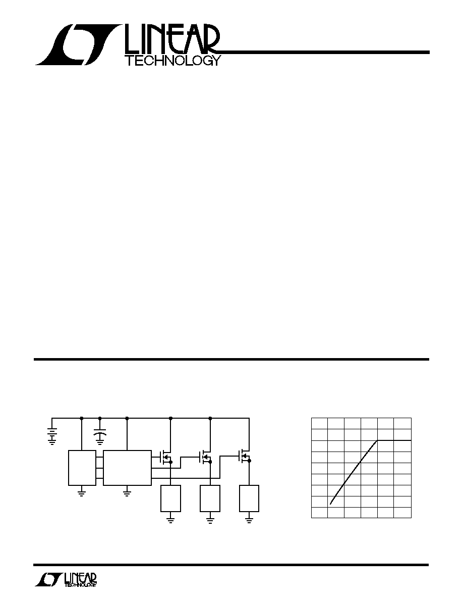
The LTC1163/LTC1165 triple low voltage MOSFET drivers
make it possible to switch supply or ground referenced
loads through inexpensive, low R
DS(ON)
N-channel switches
from as little as a 1.8V supply. The LTC1165 has inverting
inputs and makes it possible to directly replace P-channel
MOSFET switches while maintaining system drive polar-
ity. The LTC1163 has noninverting inputs.
Micropower operation, with 0.01
µ
A standby current and
95
µ
A operating current, coupled with a power supply
range of 1.8V to 6V, make the LTC1163/LTC1165 ideally
suited for 2- to 4-cell battery-powered applications. The
LTC1163/LTC1165 are also well suited for sub-3V, 3.3V
and 5V nominal supply applications.
The LTC1163/LTC1165 internal charge pumps boost the
gate voltage 8V above a 3.3V rail, fully enhancing inexpen-
sive N-channels for high- or low-side switch applications.
The LTC1163/LTC1165 are available in both an 8-pin DIP
and an 8-pin SOIC.
SUPPLY VOLTAGE (V)
0
0
GATE OUTPUT VOLTAGE (V)
2
6
8
10
4
18
LTC1163/65 · TA02
4
2
6
12
14
16
3
1
5
V
S
IN1
IN2
IN3
LTC1163
LTC1165
OUT1
OUT2
OUT3
GND
CONTROL
LOGIC
OR
µ
P
2-CELL
LOAD
2-CELL
LOAD
2-CELL
LOAD
+
+
2-CELL
BATTERY
PACK
10
µ
F
LTC1163/65 · TA01
LTC1163 HAS NONINVERTING INPUTS
LTC1165 HAS INVERTING INPUTS
(1.8V TO 3V)
RFD14N05LSM
RFD14N05LSM
RFD14N05LSM
MOSFET Switch Gate Voltage
2-Cell Triple High-Side Switch
U
S
A
O
PPLICATI
s
PCMCIA Card 3.3V/5V Switch
s
2-Cell High-Side Load Switching
s
Boost Regulator Shutdown to Zero Standby Current
s
Replacing P-Channel Switches
s
Notebook Computer Power Management
s
Palmtop Computer Power Management
s
Portable Medical Equipment
s
Mixed 3.3V and 5V Supply Switching
U
A
O
PPLICATI
TYPICAL
2
LTC1163/LTC1165
SYMBOL
PARAMETER
CONDITIONS
MIN
TYP
MAX
UNITS
I
Q
Quiescent Current OFF
V
S
= 1.8V, V
IN1
= V
IN2
= V
IN3
= V
OFF
(Note 1,2)
0.01
1
µ
A
V
S
= 3.3V, V
IN1
= V
IN2
= V
IN3
= V
OFF
(Note 1,2)
0.01
1
µ
A
V
S
= 5V, V
IN1
= V
IN2
= V
IN3
= V
OFF
(Note 1,2)
0.01
1
µ
A
Quiescent Current ON
V
S
= 1.8V, V
IN
= V
ON
(Note 2,3)
60
120
µ
A
V
S
= 3.3V, V
IN
= V
ON
(Note 2,3)
95
200
µ
A
V
S
= 5V, V
IN
= V
ON
(Note 2,3)
180
400
µ
A
V
INH
Input High Voltage
1.8V < V
S
< 2.7V
q
80%
×
V
S
V
2.7V < V
S
< 6V
q
70%
×
V
S
V
V
INL
Input Low Voltage
1.8V < V
S
< 6V
q
15%
×
V
S
V
I
IN
Input Current
0V
V
IN
V
S
q
±
1
µ
A
C
IN
Input Capacitance
5
pF
V
GATE
V
S
Gate Voltage Above Supply
V
S
= 1.8V, V
IN
= V
ON
(Note 2)
q
3.5
4.1
6.0
V
V
S
= 2V, V
IN
= V
ON
(Note 2)
q
4.0
4.6
7.0
V
V
S
= 2.2V, V
IN
= V
ON
(Note 2)
q
4.5
5.2
8.0
V
V
S
= 3.3V, V
IN
= V
ON
(Note 2)
q
6.0
8.0
9.5
V
V
S
= 5V, V
IN
= V
ON
(Note 2)
q
5.0
9.0
13.0
V
t
ON
Turn-ON Time
V
S
= 3.3V, C
GATE
= 1000pF
Time for V
GATE
> V
S
+ 1V
40
120
400
µ
s
Time for V
GATE
> V
S
+ 2V
60
180
600
µ
s
V
S
= 5V, C
GATE
= 1000pF
Time for V
GATE
> V
S
+ 1V
30
95
300
µ
s
Time for V
GATE
> V
S
+ 2V
40
130
400
µ
s
A
U
G
W
A
W
U
W
A
R
BSOLUTE
XI
TI
S
Operating Temperature Range
LTC1163C/LTC1165C ........................... 0
°
C to 70
°
C
Storage Temperature Range ................ 65
°
C to 150
°
C
Lead Temperature (Soldering, 10 sec) ................. 300
°
C
Supply Voltage ......................................................... 7V
Any Input Voltage .......................... 7V to (GND 0.3V)
Any Output Voltage ....................... 20V to (GND 0.3V)
Current (Any Pin) ................................................. 50mA
W
U
U
PACKAGE/ORDER I FOR ATIO
ORDER PART
NUMBER
ORDER PART
NUMBER
LTC1163CN8
LTC1165CN8
LTC1163CS8
LTC1165CS8
V
S
= 1.8V to 6V, T
A
= 25
°
C, unless otherwise noted.
ELECTRICAL C
C
HARA TERISTICS
LTC1163C/LTC1165C
S8 PART MARKING
1163
1165
1
2
3
4
8
7
6
5
TOP VIEW
IN1
IN2
IN3
GND
V
S
OUT1
OUT2
OUT3
N8 PACKAGE
8-LEAD PLASTIC DIP
1
2
3
4
8
7
6
5
TOP VIEW
S8 PACKAGE
8-LEAD PLASTIC SOIC
IN1
IN2
IN3
GND
V
S
OUT1
OUT2
OUT3
T
JMAX
= 100
°
C,
JA
= 130
°
C/W
T
JMAX
= 100
°
C,
JA
= 150
°
C/W
3
LTC1163/LTC1165
ELECTRICAL C
C
HARA TERISTICS
V
S
= 1.8V to 6V, T
A
= 25
°
C, unless otherwise noted.
SYMBOL
PARAMETER
CONDITIONS
MIN
TYP
MAX
UNITS
t
OFF
Turn-OFF Time
V
S
= 3.3V, C
GATE
= 1000pF
Time for V
GATE
< 0.5V
20
65
200
µ
s
V
S
= 5V, C
GATE
= 1000pF
Time for V
GATE
< 0.5V
15
45
150
µ
s
LTC1163C/LTC1165C
The
q
denotes specifications which apply over the full operating
temperature range.
Note 1: Quiescent current OFF is for all channels in OFF condition.
Note 2: LTC1163: V
OFF
= 0V, V
ON
= V
S
. LTC1165: V
OFF
= V
S
, V
ON
= 0V
Note 3: Quiescent current ON is per driver and is measured independently.
Gate Voltage Above Supply
Supply Current per Driver ON
Standby Supply Current
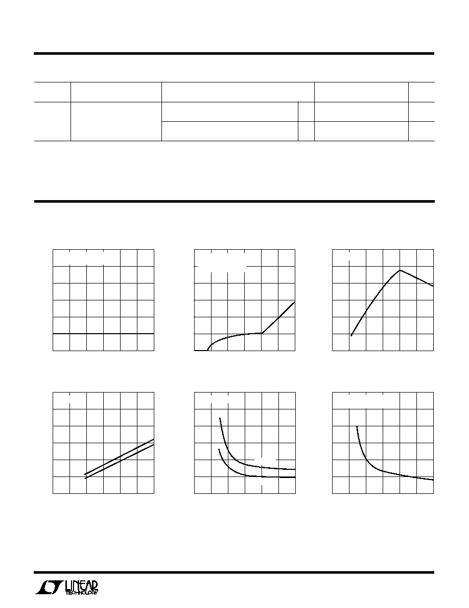
C
C
HARA TERISTICS
U
W
A
TYPICAL PERFOR
CE
SUPPLY VOLTAGE (V)
0
SUPPLY CURRENT (
µ
A)
5
4
3
2
1
0
1
1
2
3
4
LTC1163/65 · TPC01
5
6
T
A
= 25°C
ALL THREE INPUTS = OFF
SUPPLY VOLTAGE (V)
0
V
GATE
V
S
(V)
12
10
8
6
4
2
0
1
2
3
4
LTC1163/65 · TPC03
5
6
T
A
= 25°C
SUPPLY VOLTAGE (V)
0
SUPPLY CURRENT (
µ
A)
600
500
400
300
200
100
0
1
2
3
4
LTC1163/65 · TPC02
5
6
T
A
= 25°C
ONE INPUT = ON
OTHER INPUTS = OFF
Input Threshold Voltage
Turn-ON Time
Turn-OFF Time
SUPPLY VOLTAGE (V)
0
INPUT THRESHOLD VOLTAGE (V)
6
5
4
3
2
1
0
1
2
3
4
LTC1163/65 ·TPC04
5
6
T
A
= 25°C
V
HI
V
LO
SUPPLY VOLTAGE (V)
0
TURN-ON TIME (
µ
s)
600
500
400
300
200
100
0
1
2
3
4
LTC1163/65 · TPC05
5
6
C
GATE
= 1000pF
V
GS
= 2V
V
GS
= 1V
SUPPLY VOLTAGE (V)
0
TURN-OFF TIME (
µ
s)
300
250
200
150
100
50
0
1
2
3
4
LTC1163/65 · TA06
5
6
C
GATE
= 1000pF
TIME FOR V
GATE
< 0.5V
4
LTC1163/LTC1165
C
C
HARA TERISTICS
U
W
A
TYPICAL PERFOR
CE
PI FU CTIO S
U
U
U
Input Pins
The LTC1163 is noninverting; i.e., the MOSFET gate is
driven above the supply when the input pin is held high.
The LTC1165 is inverting and drives the MOSFET gate high
when the input pin is held low. The inverting inputs of the
LTC1165 allow P-channel switches to be replaced by
lower resistance/cost N-channel switches while maintain-
ing system drive polarity.
The LTC1163/LTC1165 logic inputs are high impedance
CMOS gates with ESD protection diodes to ground and
therefore should not be forced below ground. The inputs
can however, be driven above the power supply rail as
there are no clamping diodes connected between the input
pins and supply pin. This facilitates operation in mixed
5V/3V systems.
Output Pins
The output pin is either driven to ground when the switch
is turned OFF or driven above the supply rail when the
switch is turned ON. The output is clamped to about 14V
above ground by a built-in Zener clamp. This pin has a
relatively high impedance when driven above the rail (the
equivalent of a few hundred k
). Care should be taken to
minimize any loading of this pin by parasitic resistance to
ground or supply.
Supply Pin
A 150
resistor should be inserted in series with the
ground pin or supply pin if negative supply voltage tran-
sients are anticipated. This will limit the current flowing
from the power source into the LTC1163/LTC1165 to tens
of milliamps during reverse battery conditions.
OPERATIO
U
The LTC1163/LTC1165 are triple micropower MOSFET
drivers designed for operation over the 1.8V to 6V supply
range and include the following functional blocks:
3V Logic Compatible Inputs
The LTC1163/LTC1165 inputs have been designed to
accommodate a wide range of 3V and 5V logic families.
The input threshold voltage is set at roughly 50% of the
supply voltage and approximately 200mV of input hyster-
esis is provided to ensure clean switching.
The input enables all of the following circuit blocks: the
bias generator, the high frequency oscillator and gate
charge pump. Therefore, when the input is turned off, the
entire circuit powers down and the supply current drops
below 1
µ
A.
Standby Supply Current
TEMPERATURE (°C)
0
SUPPLY CURRENT (
µ
A)
5
4
3
2
1
0
1
10
20
30
40
LTC1163/65 · TPC07
50
60
70
MOSFET Gate Drive Current
GATE VOLTAGE ABOVE SUPPLY (V)
1
GATE DRIVE CURRENT (
µ
A)
10
100
1000
0
4
6
8
0.1
2
10
LTC1163/65 · TPC09
V
S
= 5V
V
S
= 3.3V
V
S
= 2.2V
V
S
= 1.8V
T
A
= 25°C
Supply Current per Driver ON
TEMPERATURE (°C)
0
SUPPLY CURRENT (
µ
A)
300
250
200
150
100
50
0
10
20
30
40
LTC1163/65 · TPC08
50
60
70
V
S
= 5V
V
S
= 3.3V
V
S
= 1.8V
5
LTC1163/LTC1165
OPERATIO
U
Gate Charge Pump
Gate drive for the power MOSFET is produced by an
internal charge pump circuit which generates a gate volt-
age substantially higher than the power supply voltage.
The charge pump capacitors are included on chip and
therefore no external components are required to generate
gate drive.
Controlled Gate Rise and Fall Times
When the input is switched ON and OFF, the gate is
charged by the internal charge pump and discharged in a
controlled manner. The charge and discharge rates have
been set to minimize RFI and EMI emissions.
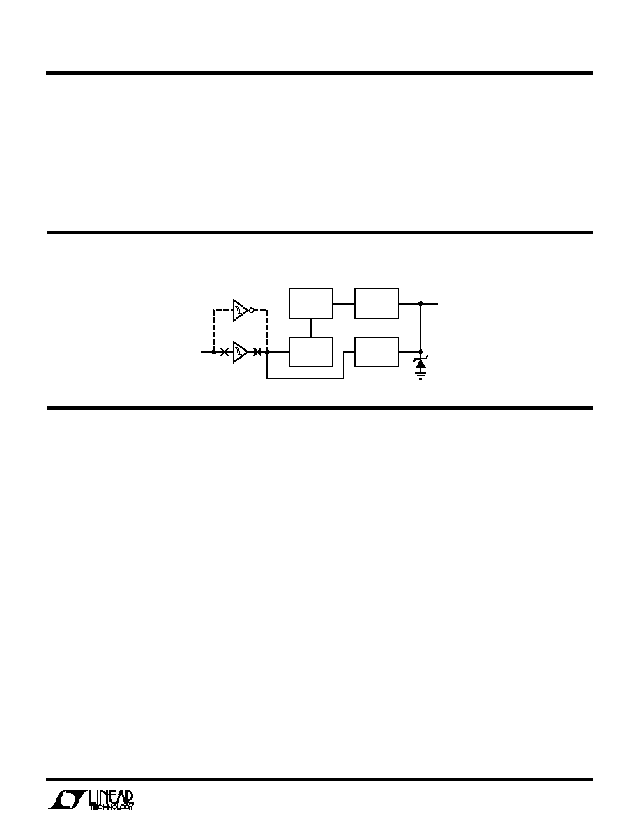
BLOCK DIAGRA
W
(One Channel)
APPLICATIO S I FOR ATIO
W
U
U
U
Logic-Level MOSFET Switches
The LTC1163/LTC1165 are designed to operate with
logic-level N-channel MOSFET switches. Although there
is some variation among manufacturers, logic-level
MOSFET switches are typically rated with V
GS
= 4V with
a maximum continuous V
GS
rating of
±
10V. R
DS(ON)
and
maximum V
DS
ratings are similar to standard MOSFETs
and there is generally little price differential. Logic-level
MOSFETs are frequently designated by an "L" and are
usually available in surface mount packaging. Some
logic-level MOSFETs are rated with V
GS
up to
±
15V and
can be used in applications which require operation over
the entire 1.8V to 6V range.
Powering Large Capacitive Loads
Electrical subsystems in portable battery-powered equip-
ment are typically bypassed with large filter capacitors to
reduce supply transients and supply induced glitching. If
not properly powered however, these capacitors may
themselves become the source of supply glitching.
For example, if a 100
µ
F capacitor is powered through a
switch with a slew rate of 0.1V/
µ
s, the current during start-
up is:
I
START
= C(
V/
t)
= (100
×
10
6
)(1
×
10
5
)
= 10A
Obviously, this is too much current for the regulator (or
output capacitor) to supply and the output will glitch by as
much as a few volts.
The startup current can be substantially reduced by limit-
ing the slew rate at the gate of an N-channel as shown in
Figure 1. The gate drive output of the LTC1163/LTC1165
is passed through a simple RC network, R1 and C1, which
substantially slows the slew rate of the MOSFET gate to
approximately 1.5
×
10
4
V/
µ
s. Since the MOSFET is
operating as a source follower, the slew rate at the source
is essentially the same as that at the gate, reducing the
startup current to approximately 15mA which is easily
LTC1163
LTC1165
LTC1163/65 · BD
GATE
DISCHARGE
LOGIC
CHARGE
PUMP
BIAS
GENERATOR
HIGH
FREQUENCY
OSCILLATOR
GATE
14V
INPUT