 | –≠–ª–µ–∫—Ç—Ä–æ–Ω–Ω—ã–π –∫–æ–º–ø–æ–Ω–µ–Ω—Ç: LTC1174 | –°–∫–∞—á–∞—Ç—å:  PDF PDF  ZIP ZIP |
1
LTC1174
LTC1174-3.3/LTC1174-5
High Efficiency
Step-Down and Inverting
DC/DC Converter
S
FEATURE
D
U
ESCRIPTIO
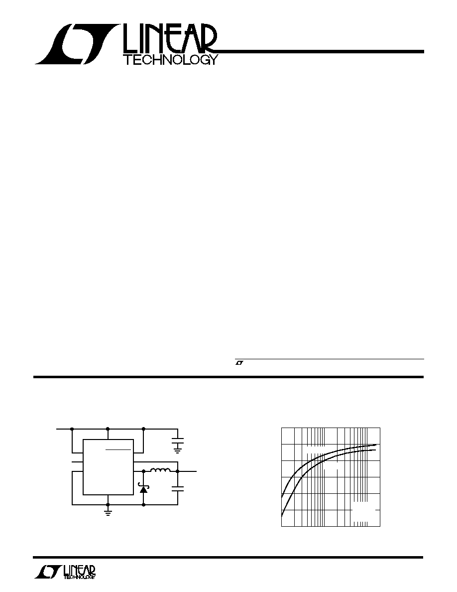
LOAD CURRENT (mA)
1
EFFICIENCY (%)
100
95
90
85
80
75
70
10
100
1174 TA02
200
V
IN
= 6V
V
IN
= 9V
L = 100
µ
H
V
OUT
= 5V
I
PGM
= 0V
High Efficiency Step-Down Converter
+
V
IN
9V
+
3
LTC1174-5
LB
IN
LB
OUT
I
PGM
GND
V
IN
SHUTDOWN
V
OUT
SW
2
7
6
8
1
5
4
100
µ
H
100
µ
F**
10V
5V
175mA
3
◊
15
µ
F*
25V
1N5818
1174 TA01
*
**
(3) AVX TPSD156K025
AVX TPSD107K010
COILTRONICS CTX100-4
LTC1174-5 Efficiency
U
A
O
PPLICATI
TYPICAL
s
High Efficiency: Up to 94%
s
Peak Inductor Current Independent of
Inductor Value
s
Short-Circuit Protection
s
Optimized for 5V to ≠ 5V Applications
s
Wide V
IN
Range: 4V to 18.5V
s
Low Dropout Operation
s
Low-Battery Detector
s
Pin Selectable Current Limit
s
Internal 0.9
Power Switch: V
IN
= 9V
s
Only Four External Components Required
s
130
µ
A Standby Current
s
Active Low Micropower Shutdown
s
Distributed Power Systems
s
Step-Down Converters
s
Inverting Converters
s
Memory Backup Supply
s
Portable Instruments
s
Battery-Powered Equipment
The LTC
Æ
1174 is a simple current mode DC/DC converter
ideally suited for 9V to 5V, 5V to 3.3V, or 5V to ≠ 5V
operation. With an internal 0.9
switch (at a supply
voltage of 9V), the LTC1174 requires only four external
components to construct a complete high efficiency
DC/DC converter.
Under a no load condition the LT1174 draws only 130
µ
A.
In shutdown, it draws a mere 1
µ
A making this converter
ideal for current sensitive applications. In dropout, the
internal P-channel MOSFET switch is turned on continu-
ously allowing the user to maximize the life of the battery
source.
The maximum inductor current of the LTC1174 family is
pin selectable to either 340mA or 600mA, optimizing
efficiency for a wide range of applications. Operation up to
200kHz permits the use of small surface mount inductors
and capacitors.
For applications requiring higher output current or ultra-
high efficiency, see the LTC1148 data sheet.
U
S
A
O
PPLICATI
and LTC are registered trademarks and LT is a trademark of Linear Technology Corporation.

2
LTC1174
LTC1174-3.3/LTC1174-5
A
U
G
W
A
W
U
W
A
R
BSOLUTE
XI
TI
S
(Voltage Referred to GND Pin)
Input Supply Voltage (Pin 6)
LTC1174 ................................................ ≠ 0.3V to 13.5V
LTC1174HV ............................................≠ 0.3V to 18.5V
Switch Current (Pin 5) ............................................... 1A
Switch Voltage (Pin 5)
LTC1174 ..................................................... V
IN
≠ 13.5V
LTC1174HV ................................................ V
IN
≠ 18.5V
Operating Temperature Range .................... 0
∞
C to 70
∞
C
Extended Commercial
Temperature Range ................................ ≠ 40
∞
C to 85
∞
C
Junction Temperature (Note 1) ............................ 125
∞
C
Storage Temperature Range ................ ≠ 65
∞
C to 150
∞
C
Lead Temperature (Soldering, 10 sec) .................. 300
∞
C
ORDER PART
NUMBER
ORDER PART
NUMBER
W
U
U
PACKAGE/ORDER I FOR ATIO
S8 PART MARKING
LTC1174CN8
LTC1174CN8-3.3
LTC1174CN8-5
LTC1174HVCN8
LTC1174HVCN8-3.3
LTC1174HVCN8-5
LTC1174IN8
LTC1174CS8
LTC1174CS8-3.3
LTC1174CS8-5
LTC1174IS8
LTC1174HVCS8
LTC1174HVCS8-3.3
LTC1174HVCS8-5
1174HV
1174H3
1174H5
1174
117433
117450
1174I
Consult factory for Military grade parts.
T
JMAX
= 125
∞
C,
JA
= 150
∞
C/W
T
JMAX
= 125
∞
C,
JA
= 110
∞
C/W
1
2
3
4
8
7
6
5
TOP VIEW
V
OUT
(V
FB
*)
LB
OUT
LB
IN
GND
SHUTDOWN
I
PGM
V
IN
SW
N8 PACKAGE
8-LEAD PLASTIC DIP
* ADJUSTABLE OUTPUT VERSION
SYMBOL PARAMETER
CONDITIONS
MIN
TYP
MAX
UNITS
I
FB
Feedback Current
LTC1174/LTC1174HV
1
µ
A
V
FB
Feedback Voltage
LTC1174/LTC1174HV
q
1.20
1.25
1.30
V
V
OUT
Regulated Output Voltage
LTC1174-3.3/LTC1174HV-3.3
q
3.14
3.30
3.46
V
LTC1174-5/LTC1174HV-5
q
4.75
5.00
5.25
V
V
OUT
Output Voltage Line Regulation
V
IN
= 6V to 12V, I
LOAD
= 100mA, I
PGM
= V
IN
(Note 2)
10
70
mV
Output Voltage Load Regulation
LTC1174-3.3 (Note 2)
20mA < I
LOAD
< 175mA, I
PGM
= 0V
≠ 5
≠ 70
mV
20mA < I
LOAD
< 400mA, I
PGM
= V
IN
≠ 45
≠ 70
mV
LTC1174-5 (Note 2)
20mA < I
LOAD
< 175mA, I
PGM
= 0V
≠ 5
≠ 70
mV
20mA < I
LOAD
< 400mA, I
PGM
= V
IN
≠ 50
≠ 70
mV
ELECTRICAL C
C
HARA TERISTICS
T
A
= 25
∞
C, V
IN
= 9V, V
SHUTDOWN
= V
IN
, I
PGM
= 0V, unless otherwise noted.
1
2
3
4
8
7
6
5
TOP VIEW
S8 PACKAGE
8-LEAD PLASTIC SOIC
* ADJUSTABLE OUTPUT VERSION
V
OUT
(V
FB
*)
LB
OUT
LB
IN
GND
SHUTDOWN
I
PGM
V
IN
SW

3
LTC1174
LTC1174-3.3/LTC1174-5
ELECTRICAL C
C
HARA TERISTICS
T
A
= 25
∞
C, V
IN
= 9V, V
SHUTDOWN
= V
IN
, I
PGM
= 0V, unless otherwise noted.
≠ 40
∞
C
T
A
85
∞
C (Note 6), for LTC1174I only.
SYMBOL PARAMETER
CONDITIONS
MIN
TYP
MAX
UNITS
V
FB
Feedback Voltage
LTC1174I
1.18
1.25
1.31
V
I
LBOUT
Current Sunk by Pin 2
V
LBOUT
= 0.4
0.75
1.2
2
mA
I
PEAK
Current Limit
I
PGM
= V
IN
, V
OUT
= 0V
0.54
0.60
0.78
A
I
PGM
= 0V, V
OUT
= 0V
0.34
A
t
OFF
Switch Off-Time (Note 5)
V
OUT
at Regulated Value
2
4
6
µ
s
The
q
denotes specifications which apply over the full operating
temperature range.
Note 1: T
J
is calculated from the ambient temperature T
A
and power
dissipation P
D
according to the following formulas:
LTC1174CN8, LTC1174CN8-3.3, LTC1174CN8-5:
T
J
= T
A
+ (P
D
◊
110
∞
C/W)
LTC1174CS8, LTC1174CS8-3.3, LTC1174CS8-5:
T
J
= T
A
+ (P
D
◊
150
∞
C/W)
Note 2: Guaranteed by design.
Note 3: Dynamic supply current is higher due to the gate charge being
delivered at the switching frequency.
Note 4: Current into pin 6 only, measured without electrolytic input
capacitor.
Note 5: The off-time is wafer-sort trimmed.
Note 6: The LTC1174I is not tested and not quality assurance sampled at
≠ 40
∞
C and 85
∞
C. These specifications are guaranteed by design and/or
correlation.
SYMBOL PARAMETER
CONDITIONS
MIN
TYP
MAX
UNITS
I
Q
Input DC Supply Current (Note 3)
Active Mode
LTC1174: 4V < V
IN
< 12V, I
PGM
= 0V
450
600
µ
A
LTC1174HV: 4V < V
IN
< 16V, I
PGM
= 0V
450
600
µ
A
Sleep Mode
LTC1174: 4V < V
IN
< 12V
130
180
µ
A
LTC1174HV: 4V < V
IN
< 16V
130
180
µ
A
SHUTDOWN (Note 4)
LTC1174: V
SHUTDOWN
= 0V, 4V < V
IN
< 12V
1
10
µ
A
LTC1174HV: V
SHUTDOWN
= 0V, 4V < V
IN
< 16V
2
25
µ
A
V
LBTRIP
Low-Battery Trip Point
1.25
1.4
V
I
LBIN
Current into Pin 3
0.5
µ
A
I
LBOUT
Current Sunk by Pin 2
LTC1174: V
LBOUT
= 0.4V
1.0
1.2
1.5
mA
LTC1174HV: V
LBOUT
= 0.4V
0.6
0.8
1.5
mA
V
HYST
Comparator Hysteresis
LTC1174/LTC1174HV
7.5
15
30
mV
I
PEAK
Current Limit
I
PGM
= V
IN
, V
OUT
= 0V
q
0.54
0.60
0.78
A
I
PGM
= 0V, V
OUT
= 0V
q
0.27
0.34
0.50
A
R
ON
ON Resistance of Switch
LTC1174
q
0.75
1.30
LTC1174HV
q
0.90
1.55
t
OFF
Switch Off-Time (Note 5)
V
OUT
at Regulated Value
3
4
5
µ
s
V
IH
SHUTDOWN Pin High
Minimum Voltage at Pin 8 for Device to Be Active
1.2
V
V
IL
SHUTDOWN Pin Low
Maximum Voltage at Pin 8 for Device to Be in Shutdown
0.75
V
I
IH
SHUTDOWN Pin Input Current
LTC1174: V
SHUTDOWN
= 12V
0.5
µ
A
LTC1174HV: V
SHUTDOWN
= 16V
2.0
I
IL
SHUTDOWN Pin Input Current
0
V
SHUTDOWN
0.8V
0.5
µ
A
4
LTC1174
LTC1174-3.3/LTC1174-5
C
C
HARA TERISTICS
U
W
A
TYPICAL PERFOR
CE
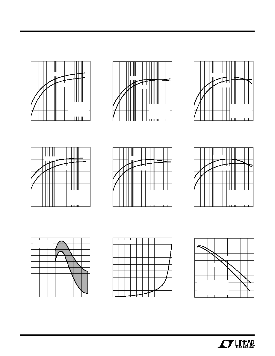
LOAD CURRENT (mA)
1
EFFICIENCY (%)
100
95
90
85
80
75
70
10
100
1174 G01
200
V
IN
= 6V
V
IN
= 9V
L = 50
µ
H
V
OUT
= 5V
I
PGM
= 0V
COIL = CTX50-4
Efficiency vs Load Current
Efficiency vs Load Current
LOAD CURRENT (mA)
1
EFFICIENCY (%)
10
100
1174 G02
400
100
95
90
85
80
75
70
L = 50
µ
H
V
OUT
= 5V
I
PGM
= V
IN
COIL = CTX50-4
V
IN
= 6V
V
IN
= 9V
LOAD CURRENT (mA)
1
EFFICIENCY (%)
10
100
1174 G03
500
100
95
90
85
80
75
70
L = 100
µ
H
V
OUT
= 5V
I
PGM
= V
IN
COIL = CTX100-4
V
IN
= 6V
V
IN
= 9V
Efficiency vs Load Current
Efficiency vs Load Current
Efficiency vs Load Current
LOAD CURRENT (mA)
1
EFFICIENCY (%)
10
100
1174 G04
300
100
90
80
70
60
50
L = 50
µ
H
V
OUT
= 3.3V
I
PGM
= 0V
COIL = CTX50-4
V
IN
= 5V
V
IN
= 9V
Efficiency vs Load Current
LOAD CURRENT (mA)
1
EFFICIENCY (%)
10
100
1174 G05
500
100
90
80
70
60
50
L = 50
µ
H
V
OUT
= 3.3V
I
PGM
= V
IN
COIL = CTX50-4
V
IN
= 5V
V
IN
= 9V
LOAD CURRENT (mA)
1
EFFICIENCY (%)
10
100
1174 G06
500
100
90
80
70
60
50
L = 100
µ
H
V
OUT
= 3.3V
I
PGM
= V
IN
COIL = CTX100-4
V
IN
= 5V
V
IN
= 9V
Line Regulation
Switch Leakage Current
vs Temperature
TEMPERATURE (∞C)
0
LEAKAGE CURRENT (nA)
180
160
140
120
100
80
60
40
20
0
40
80
100
1174 G08
20
60
V
IN
= 13.5V
INPUT VOLTAGE (V)
5
EFFICIENCY (%)
14
1174 G09
7
9
12
95
94
93
92
91
90
89
88
87
6
8
10
11
13
L = 100
µ
H
L = 50
µ
H
V
OUT
= 5V
I
PGM
= 0V
I
LOAD
= 75mA
CORE = CTX (Kool M
µ
Æ
)
Efficiency vs Input Voltage
Kool M
µ
Æ
is a registered trademark of Magnetics, Inc.
INPUT VOLTAGE (V)
0
V
OUT
(mV)
6
4
2
0
≠ 2
≠ 4
≠ 6
≠ 8
≠10
≠12
≠14
4
8
10
1174 G07
2
6
12
14
I
LOAD
= 100mA
I
PGM
= 0V
5
LTC1174
LTC1174-3.3/LTC1174-5
C
C
HARA TERISTICS
U
W
A
TYPICAL PERFOR
CE
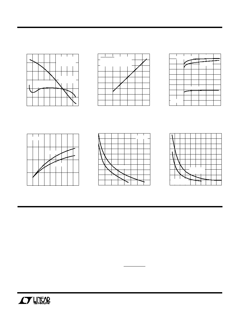
Supply Current in Shutdown
Switch Resistance vs
Input Voltage
INPUT VOLTAGE (V)
0
SUPPLY CURRENT (
µ
A)
8
1.8
1.6
1.4
1.2
1.0
0.8
0.6
0.4
0.2
0
1174 G11
4
14
2
6
10
12
SHUTDOWN = 0V
T
A
= 25∞C
CURRENT INTO PIN 6 ONLY
INPUT VOLTAGE (V)
5
EFFICIENCY (%)
7
9
10
14
1174 G10
6
8
11
12
13
95
94
93
92
91
90
89
V
OUT
= 5V
L = 100
µ
H
COIL = CTX100-4
I
LOAD
= 300mA
I
PGM
= V
IN
I
LOAD
= 100mA
I
PGM
= 0V
Efficiency vs Input Voltage
DC Supply Current
INPUT VOLTAGE (V)
0
SUPPLY CURRENT (
µ
A)
500
450
400
350
300
250
200
150
100
50
0
4
8
10
1174 G12
2
6
12
14
ACTIVE MODE
I
PGM
= V
IN
SLEEP MODE
I
PGM
= 0V
T
A
= 25∞C
Operating Frequency
vs V
IN
≠ V
OUT
(V
IN
≠ V
OUT
) VOLTAGE (V)
0
NORMALIZED FREQUENCY
9
1174 G13
2
5
7
2.0
1.5
1.0
0.5
0
1
3
4
6
8
V
OUT
= 5V
T
A
= 25∞C
T
A
= 70∞C
Off-Time vs Output Voltage
SW (Pin 5): Drain of the P-Channel MOSFET Switch. Cathode
of Schottky diode must be closely connected to this pin.
V
IN
(Pin 6): Input Supply Voltage. It must be decoupled
close to ground pin 4.
I
PGM
(Pin 7): Selects the Current Limit of the P-Channel
Switch. With I
PGM
= V
IN
, the current trip point is 600mA and
with I
PGM
= 0V, the current trip value is reduced to 340mA.
SHUTDOWN (Pin 8): Pulling this pin to ground keeps the
internal switch off and puts the LTC1174 in micropower
shutdown.
PI FU CTIO S
U
U
U
V
OUT
(V
FB
) (Pin 1): For the LTC1174, this pin connects to the
main voltage comparator's input. On the LTC1174-3.3 and
LTC1174-5 this pin goes to an internal resistive divider
which sets the output voltage.
LB
OUT
(Pin 2): Open Drain of an N-Channel Pull-Down. This
pin will sink current when pin 3 (LB
IN
) goes below 1.25V.
During shutdown this pin goes to high impedance.
LB
IN
(Pin 3): The "≠" Input of the Low-Battery Voltage
Comparator. The "+" input is connected to a reference
voltage of 1.25V.
GND (Pin 4): Ground Pin.
OUTPUT VOLTAGE (V)
0
OFF-TIME (
µ
s)
50
40
30
20
10
0
4
1174 G15
1
2
3
5
LTC1174-5
LTC1174HV-5
LTC1174-3.3
LTC1174HV-3.3
INPUT VOLTAGE (V)
4
RDS
(ON)
(
)
12
1174 G14
6
8
10
14
16
18
20
T
A
= 25∞C
1.7
1.6
1.5
1.4
1.3
1.2
1.1
1.0
0.9
0.8
0.7
LTC1174HV
LTC1174