 | ÐлекÑÑоннÑй компоненÑ: LTC1255 | СкаÑаÑÑ:  PDF PDF  ZIP ZIP |
Äîêóìåíòàöèÿ è îïèñàíèÿ www.docs.chipfind.ru
1
LTC1255
Dual 24V High-Side
MOSFET Driver
The LTC1255 dual high-side driver allows using low
cost N-channel FETs for high-side industrial and auto-
motive switching applications. An internal charge pump
boosts the gate drive voltage above the positive rail,
fully enhancing an N-channel MOS switch with no
external components. Low power operation, with 12
µ
A
standby current, allows use in virtually all systems with
maximum efficiency.
Included on-chip is independent overcurrent sensing
to provide automatic shutdown in case of short circuits.
A time delay can be added to the current sense to
prevent false triggering on high in-rush current loads.
The LTC1255 operates from 9V to 24V supplies and is
well suited for industrial and automotive applications.
The LTC1255 is available in both an 8-pin DIP and an
8-pin SOIC.
S
FEATURE
s
Fully Enhances N-Channel Power MOSFETs
s
12
µ
A Standby Current
s
Operates at Supply Voltages from 9V to 24V
s
Short Circuit Protection
s
Easily Protected Against Supply Transients
s
Controlled Switching ON and OFF Times
s
No External Charge Pump Components
s
Compatible With Standard Logic Families
s
Available in 8-Pin SOIC
U
S
A
O
PPLICATI
s
Solenoid Drivers
s
DC Motor Drivers
s
Stepper Motor Drivers
s
Lamp Drivers/Dimmers
s
Relay Drivers
s
Low Frequency H-Bridge
s
P-Channel Switch Replacement
D
U
ESCRIPTIO
U
A
O
PPLICATI
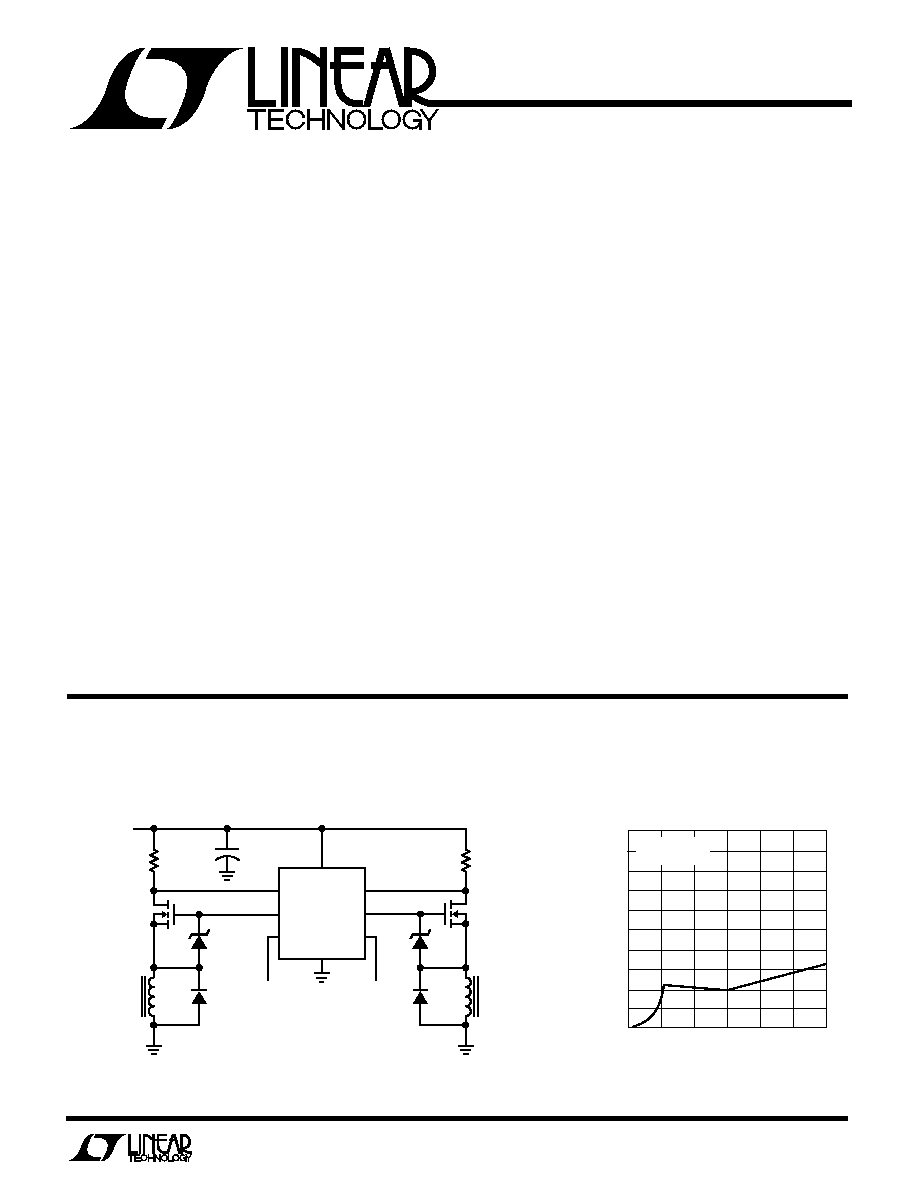
TYPICAL
12V
1N4001
+
10
µ
F
IRLR024
24V
24V/0.5A
SOLENOID
V
S
DS2
LTC1255
IN2
GND
DS1
IN1
G1
G2
0.036
0.036
IRLR024
12V
1N4001
24V/0.5A
SOLENOID
FROM
µ
P, ETC.
FROM
µ
P, ETC.
LTC1255 · TA01
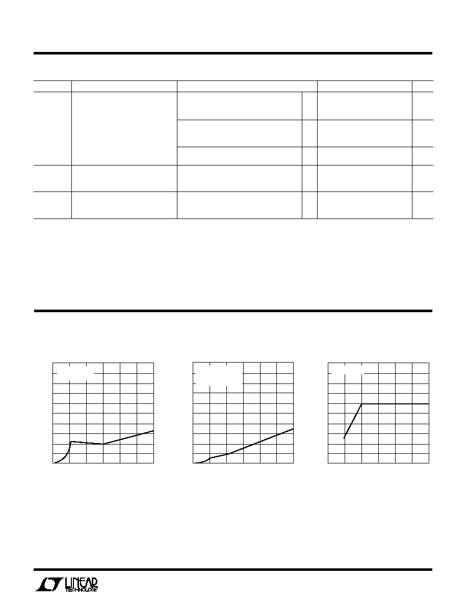
Standby Supply Current
Dual 24V High-Side Switch with Overcurrent Protection
SUPPLY VOLTAGE (V)
0
0
SUPPLY CURRENT
(
µ
A)
10
15
20
25
30
35
5
10
15
20
LTC1255 · TA02
25
40
45
50
5
30
V
IN1
= V
IN2
= 0V
T
A
= 25°C
2
LTC1255
Supply Voltage ......................................... 0.3V to 30V
Transient Supply Voltage (< 10ms) ......................... 40V
Input Voltage ..................... (V
S
+ 0.3V) to (GND 0.3V)
Gate Voltage ...................... (V
S
+ 20V) to (GND 0.3V)
Current (Any Pin) ................................................. 50mA
A
U
G
W
A
W
U
W
A
R
BSOLUTE
XI
TI
S
Operating Temperature Range
LTC1255C ............................................... 0
°
C to 70
°
C
LTC1255I ........................................... 40
°
C to 85
°
C
Storage Temperature Range ................ 65
°
C to 150
°
C
Lead Temperature (Soldering, 10 sec) ................. 300
°
C
W
U
U
PACKAGE/ORDER I FOR ATIO
ORDER PART
NUMBER
ORDER PART
NUMBER
T
JMAX
= 100
°
C,
JA
= 130
°
C/ W
T
JMAX
= 100
°
C,
JA
= 150
°
C/ W
1
2
3
4
8
7
6
5
TOP VIEW
DS1
GATE 1
GND
IN1
DS2
GATE 2
V
S
IN2
N8 PACKAGE
8-LEAD PLASTIC DIP
1
2
3
4
8
7
6
5
TOP VIEW
DS2
GATE 2
V
S
IN2
DS1
GATE 1
GND
IN1
S8 PACKAGE
8-LEAD PLASTIC SOIC
SYMBOL
PARAMETER
CONDITIONS
MIN
TYP
MAX
UNITS
I
Q
Quiescent Current OFF
V
S
= 10V, V
IN
= 0V (Note 1)
12
40
µ
A
V
S
= 18V, V
IN
= 0V (Note 1)
12
40
µ
A
V
S
= 24V, V
IN
= 0V (Note 1)
12
40
µ
A
Quiescent Current ON
V
S
= 10V, V
GATE
= 22V, V
IN
= 5V (Note 2)
160
400
µ
A
V
S
= 18V, V
GATE
= 30V, V
IN
= 5V (Note 2)
350
800
µ
A
V
S
= 24V, V
GATE
= 36V, V
IN
= 5V (Note 2)
600
1200
µ
A
V
INH
Input High Voltage
q
2
V
V
INL
Input Low Voltage
q
0.8
V
I
IN
Input Current
0V
V
IN
V
S
q
±
1
µ
A
C
IN
Input Capacitance
5
pF
V
SEN
Drain Sense Threshold Voltage
80
100
120
mV
q
75
100
125
mV
I
SEN
Drain Sense Input Current
0V
V
SEN
V
S
q
±
0.1
µ
A
V
GATE
V
S
Gate Voltage Above Supply
V
S
= 9V
q
7.5
10.5
12
V
I
GATE
Gate Output Drive Current
V
S
= 18V, V
GATE
= 30V
q
5
20
µ
A
V
S
= 24V, V
GATE
= 36V
q
5
23
µ
A
ELECTRICAL C
C
HARA TERISTICS
V
S
= 9V to 24V, T
A
= 25
°
C, unless otherwise noted.
LTC1255CN8
LTC1255IN8
S8 PART MARKING
LTC1255CS8
LTC1255IS8
1255
1255I
3
LTC1255
SYMBOL
PARAMETER
CONDITIONS
MIN
TYP
MAX
UNITS
t
ON
Turn-ON Time
V
S
= 10V, C
GATE
= 1000pF (Note 3)
Time for V
GATE
> V
S
+ 2V
30
100
300
µ
s
Time for V
GATE
> V
S
+ 5V
75
250
750
µ
s
V
S
= 18V, C
GATE
= 1000pF (Note 3)
Time for V
GATE
> V
S
+ 5V
40
120
400
µ
s
Time for V
GATE
> V
S
+ 10V
75
250
750
µ
s
V
S
= 24V, C
GATE
= 1000pF (Note 3)
Time for V
GATE
> V
S
+ 10V
50
180
500
µ
s
t
OFF
Turn-OFF Time
V
S
= 10V, C
GATE
= 1000pF, (Note 3, 4)
10
24
60
µ
s
V
S
= 18V, C
GATE
= 1000pF, (Note 3, 4)
10
21
60
µ
s
V
S
= 24V, C
GATE
= 1000pF, (Note 3, 4)
10
19
60
µ
s
t
SC
Short-Circuit Turn-OFF Time
V
S
= 10V, C
GATE
= 1000pF, (Note 3, 4)
5
16
30
µ
s
V
S
= 18V, C
GATE
= 1000pF, (Note 3, 4)
5
16
30
µ
s
V
S
= 24V, C
GATE
= 1000pF, (Note 3, 4)
5
16
30
µ
s
V
S
= 9V to 24V, T
A
= 25
°
C, unless otherwise noted.
ELECTRICAL C
C
HARA TERISTICS
The
q
denotes specifications which apply over the full operating
temperature range.
Note 1: Quiescent current OFF is for both channels in OFF condition.
Note 2: Quiescent current ON is per driver and is measured independently.
The gate voltage is clamped to 12V above the rail to simulate the effects of
protection clamps connected across the GATE-SOURCE of the power
MOSFET.
Note 3: Zener diode clamps must be connected across the GATE-SOURCE
of the power MOSFET to limit V
GS
. 1N5242A (through hole) or
MMBZ5242A (surface mount) 12V Zener diodes are recommended. All
Turn-ON and Turn-OFF tests are performed with a 12V Zener clamp in
series with a small-signal diode connected between V
S
and the GATE
output to simulate the effects of a 12V protection Zener clamp connected
across the GATE-SOURCE of the power MOSFET.
Note 4: Time for V
GATE
to drop below 1V.
C
C
HARA TERISTICS
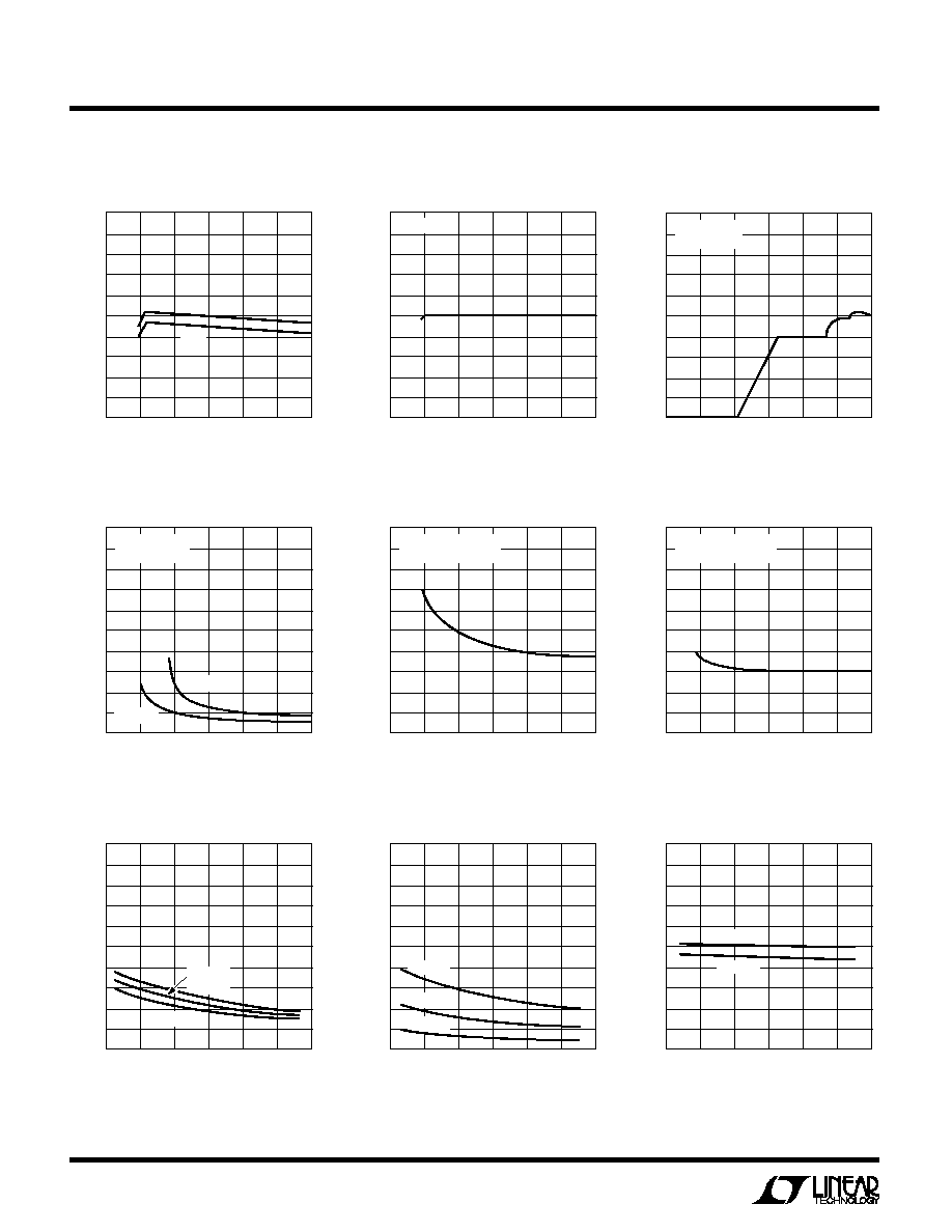
U
W
A
TYPICAL PERFOR
CE
Standby Supply Current
Gate Voltage Above Supply
Supply Current per Driver (ON)
SUPPLY VOLTAGE (V)
0
0
V
GATE
V
S
(V)
4
6
8
10
12
14
5
10
15
20
LTC1255 · TPC03
25
16
18
20
2
30
V
CLAMP
= 12V
SUPPLY VOLTAGE (V)
0
0
SUPPLY CURRENT (mA)
0.4
0.6
0.8
1.0
1.2
1.4
5
10
15
20
LTC1255 · TPC02
25
1.6
1.8
2.0
0.2
30
ONE INPUT = 0N
OTHER INPUT = OFF
T
A
= 25°C
SUPPLY VOLTAGE (V)
0
0
SUPPLY CURRENT (
µ
A)
10
15
20
25
30
35
5
10
15
20
LTC1255 · TPC01
25
40
45
50
5
30
V
IN1
= V
IN2
= 0V
T
A
= 25°C
4
LTC1255
C
C
HARA TERISTICS
U
W
A
TYPICAL PERFOR
CE
Input Threshold Voltage
Short-Circuit Turn-OFF Delay Time
Turn-ON Time
Standby Supply Current
Supply Current per Channel (ON)
Input ON Threshold
Gate Clamp Current
Drain Sense Threshold Voltage
Turn-OFF Time
SUPPLY VOLTAGE (V)
0
0.4
INPUT THRESHOLD VOLTAGE (V)
0.8
1.0
1.2
1.4
1.6
1.8
5
10
15
20
LTC1255 · TPC04
25
2.0
2.2
2.4
0.6
30
V
ON
V
OFF
SUPPLY VOLTAGE (V)
0
75
DRAIN SENSE THRESHOLD VOLTAGE (V)
85
90
95
100
105
110
5
10
15
20
LTC1255 · TPC05
25
115
120
125
80
30
T
A
= 25°C
SUPPLY VOLTAGE (V)
0
0
GATE CLAMP CURRENT (
µ
A)
10
15
20
25
30
35
5
10
15
20
LTC1255 · TA06
25
40
45
50
5
30
V
CLAMP
= 12V
T
A
= 25°C
SUPPLY VOLTAGE (V)
0
0
TURN-ON TIME (
µ
s)
200
300
400
500
600
700
5
10
15
20
LTC1255 · TA07
25
800
900
1000
100
30
C
GATE
= 1000pF
T
A
= 25°C
V
GS
= 5V
V
GS
= 2V
SUPPLY VOLTAGE (V)
0
0
TURN-OFF TIME (
µ
s)
10
15
20
25
30
35
5
10
15
20
LTC1255 · TA08
25
40
45
50
5
30
C
GATE
= 1000pF
TIME FOR V
GATE
< 1V
SUPPLY VOLTAGE (V)
0
0
TURN-OFF TIME (
µ
s)
10
15
20
25
30
35
5
10
15
20
LTC1255 · TA09
25
40
45
50
5
30
C
GATE
= 1000pF
TIME FOR V
GATE
< 1V
TEMPERATURE (°C)
50
0
STANDBY SUPPLY CURRENT (
µ
A)
10
15
20
25
30
35
25
0
25
50
LTC1255 · TA10
75
40
45
50
5
100
V
S
= 10V
V
S
= 18V
V
S
= 24V
TEMPERATURE (°C)
50
0.4
INPUT THRESHOLD VOLTAGE (V)
0.8
1.0
1.2
1.4
1.6
1.8
25
0
25
50
LTC1255 · TA12
75
2.0
2.2
2.4
0.6
100
V
S
= 10V
V
S
= 24V
TEMPERATURE (°C)
50
0
SUPPLY CURRENT (mA)
0.4
0.6
0.8
1.0
1.2
1.4
25
0
25
50
LTC1255 · TA11
75
1.6
1.8
2.0
0.2
100
V
S
= 24V
V
S
= 10V
V
S
= 18V

5
LTC1255
PI FU CTIO S
U
U
U
Input Pin
The LTC1255 input pin is active high and activates all of
the protection and charge pump circuitry when switched
ON. The LTC1255 logic and shutdown inputs are high
impedance CMOS gates with ESD protection diodes to
ground and supply and therefore should not be forced
beyond the power supply rails. The input pin should be
held low during the application of power to properly set
the input latch.
Gate Drive Pin
The gate drive pin is either driven to ground when the
switch is turned OFF or driven above the supply rail
when the switch is turned ON. This pin is of relatively
high impedance when driven above the rail (the equiva-
lent of a few hundred k
). Care should be taken to
minimize any loading of this pin by parasitic resistance
to ground or supply.
Supply Pin
The supply pin of the LTC1255 serves two vital pur-
poses. The first is obvious; it powers the input, gate
drive, regulation and protection circuitry. The second
purpose is less obvious; it provides a Kelvin connection
to the top of the drain sense resistor for the internal
100mV reference.
The supply pin of the LTC1255 should never be forced
below ground as this may result in permanent damage
to the device. A 100
resistor should be inserted in
series with the ground pin if negative supply voltage
transients are anticipated.
The LTC1255 is designed to be continuously powered
so that the gate of the MOSFET is actively driven at all
times. If it is necessary to remove power from the
supply pin and then reapply it, the input pin should be
cycled (low to high) a few milliseconds
after the power
is reapplied to reset the input latch and protection
circuitry. Also, the input pin should be isolated from the
controlling logic by a 10k resistor if there is a possibility
that the input pin will be held high after the supply has
been removed.
Drain Sense Pin
The drain sense pin is compared against the supply pin
voltage. If the voltage at this pin is more than 100mV
below the supply pin, the input latch will be reset and
the MOSFET gate will be quickly discharged. Cycle the
input to reset the short-circuit latch and turn the MOSFET
back on.
This pin is also a high impedance CMOS gate with ESD
protection and therefore should not be forced outside
of the power supply rails. To defeat the overcurrent
protection, short the drain sense pin to the supply pin.
Some loads, such as large supply capacitors, lamps or
motors require high in-rush currents. An RC time delay
can be added between the sense resistor and the drain
sense pin to ensure that the drain sense circuitry does
not false trigger during startup. This time constant can
be set from a few microseconds to many seconds.
However, very long delays may put the MOSFET at risk
of being destroyed by a short-circuit condition (see
Applications Information section).
OPERATIO
U
The LTC1255 is a dual 24V MOSFET driver with built-in
protection and gate charge pump. The LTC1255 consists
of the following functional blocks:
TTL and CMOS Compatible Inputs and Latches
The LTC1255 inputs have been designed to accommo-
date a wide range of logic families. Both input thresh-
olds are set at about 1.3V with approximately 100mV of
hysteresis. A low standby current regulator provides
continuous bias for the TTL-to-CMOS converter.
The input/protection latch should be set after initial
power-up, or after reapplication of power, by cycling
the input low to high.