 | ÐлекÑÑоннÑй компоненÑ: LTC1266 | СкаÑаÑÑ:  PDF PDF  ZIP ZIP |
Äîêóìåíòàöèÿ è îïèñàíèÿ www.docs.chipfind.ru
1
LTC1266
LTC1266-3.3/LTC1266-5
Synchronous Regulator
Controller for
N- or P-Channel MOSFETs
S
FEATURE
D
U
ESCRIPTIO
s
Ultra-High Efficiency: Over 95% Possible
s
Drives N-Channel MOSFET for High Current or
P-Channel MOSFET for Low Dropout
s
Pin Selectable Burst Mode Operation
s
1% Output Accuracy (LTC1266A)
s
Pin Selectable Phase of Topside Driver for Boost
or Step-Down Operation
s
Wide V
IN
Range: 3.5V to 20V
s
On-Chip Low-Battery Detector
s
High Efficiency Maintained over Large Current Range
s
Low 170
µ
A Standby Current at Light Loads
s
Current Mode Operation for Excellent Line and Load
Transient Response
s
Logic Controlled Micropower Shutdown: I
Q
< 40
µ
A
s
Short Circuit Protection
s
Synchronous Switching with Nonoverlaping Gate Drives
s
Available in 16-Pin Narrow SO Package
The LTC
®
1266 series is a family of synchronous switching
regulator controllers featuring automatic Burst Mode
TM
operation to maintain high efficiencies at low output
currents. These devices drive external power MOSFETs at
switching frequencies up to 400kHz using a constant off-
time current mode architecture providing constant ripple
current in the inductor. They can drive either an N-channel
or a P-channel topside MOSFET.
The operating current level is user-programmable via an
external current sense resistor. Wide input supply range
allows operation from 3.5V to 18V (20V maximum).
Constant off-time architecture provides low dropout regu-
lation limited only by the R
DS(ON)
of the topside MOSFET
(when using the P-channel) and the resistance of the
inductor and current sense resistor.
The LTC1266 series combines synchronous switching for
maximum efficiency at high currents with an automatic
low current operating mode, called Burst Mode
operation,
which reduces switching losses. Standby power is re-
duced to only 1mW at V
IN
= 5V (at I
OUT
= 0). Load currents
in Burst Mode
operation are typically 0mA to 500mA.
, LTC and LT are registered trademarks of Linear Technology Corporation.
Burst Mode is a trademark of Linear Technology Corporation.
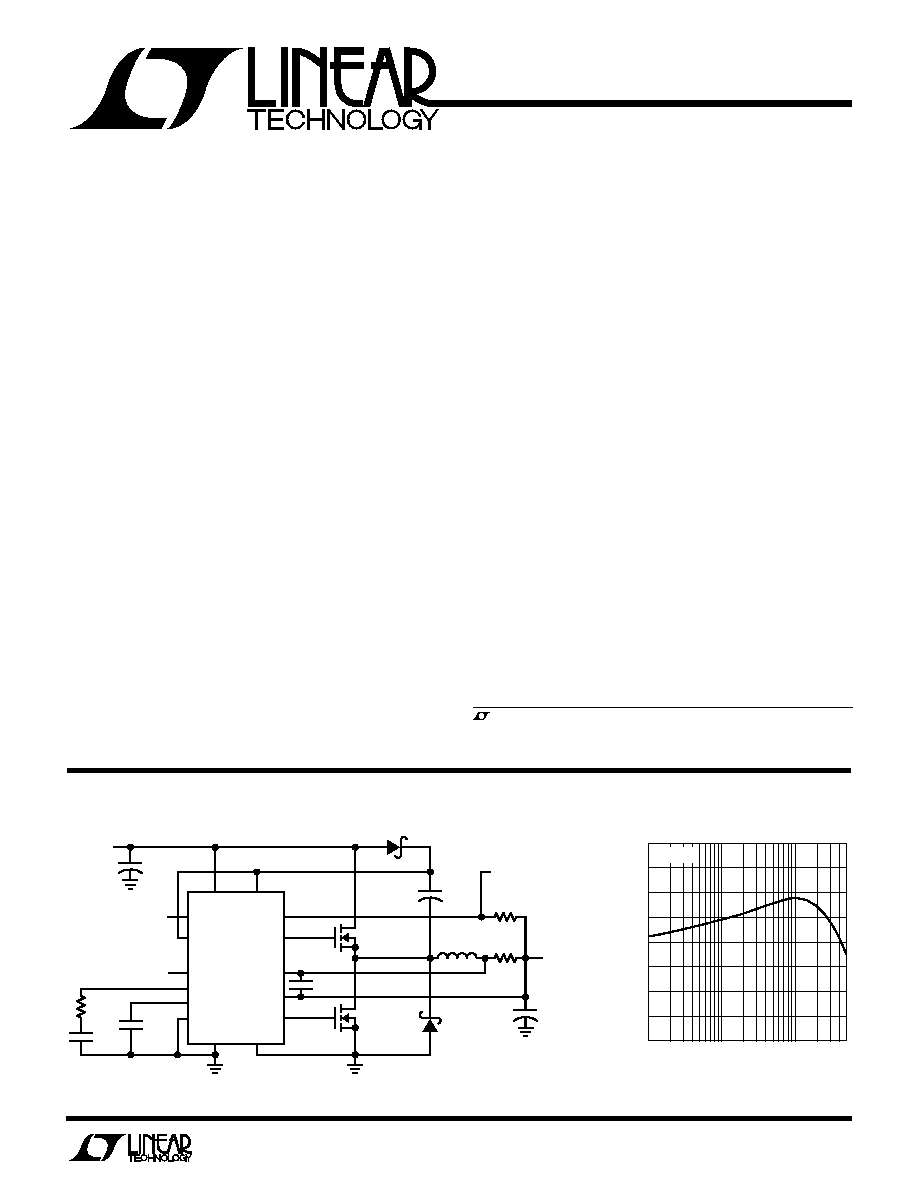
Figure 1. High Efficiency Step-Down Converter
LTC1266-3.3 Efficiency
LOAD CURRENT (A)
0.01
80
EFFICIENCY (%)
85
90
95
100
0.1
5
1
LTC1266 · TA02
V
IN
= 5V
0V = NORMAL
>1.5V = SHUTDOWN
N-CHANNEL
Si9410
+
C
IN
100
µ
F
×
2
L*
5
µ
H
D2
MBR0530T1
R
SENSE
0.02
100k
V
OUT
3.3V
5A
LOW BAT OUT
V
IN
4V TO 9V
I
TH
C
T
SGND
C
T
180pF
C
C
3300pF
R
C
470
+
C
OUT
330
µ
F
×
2
D1
MBRS130LT3
LTC1266 · TA01
BDRIVE
BINH
PGND
N-CHANNEL
Si9410
V
IN
PWR V
IN
LB
OUT
LB
IN
PINV
LTC1266-3.3
SHDN
SENSE
+
TDRIVE
SENSE
1000pF
C
B
0.1
µ
F
*COILTRONICS CTXO212801
LOW BAT IN
s
Notebook and Palmtop Computers
s
Portable Instruments
s
Cellular Telephones
s
DC Power Distribution Systems
s
GPS Systems
U
S
A
O
PPLICATI
U
A
O
PPLICATI
TYPICAL
2
LTC1266
LTC1266-3.3/LTC1266-5
A
U
G
W
A
W
U
W
A
R
BSOLUTE
XI
TI
S
Input Supply Voltage (Pins 2, 5) ............... 20V to 0.3V
Continuous Output Current (Pins 1, 16) .............. 50mA
Sense Voltages (Pins 8, 9)........................ 13V to 0.3V
PINV, BINH, SHDN, LB
IN
(Pins 3, 4, 11, 13) ................................. 20V to 0.3V
LB
OUT
Output Current ........................................... 12mA
Operating Ambient Temperature Range ...... 0
°
C to 70
°
C
Extended Commercial
Temperature Range ........................... 40
°
C to 85
°
C
Junction Temperature (Note 1) ............................ 125
°
C
Storage Temperature Range ................ 65
°
C to 150
°
C
Lead Temperature (Soldering, 10 sec) ................. 300
°
C
W
U
U
PACKAGE/ORDER I FOR ATIO
ORDER PART
NUMBER
LTC1266CS
LTC1266CS-3.3
LTC1266CS-5
LTC1266ACS
SYMBOL
PARAMETER
CONDITIONS
MIN
TYP
MAX
UNITS
V
FB
Feedback Voltage
V
IN
= 9V, I
LOAD
= 700mA, V
PINV
= V
PWR
,
LTC1266ACS
Topside Switch = N-Ch
q
1.275
V
LTC1266CS
q
1.210
1.25
1.290
V
I
FB
Feedback Current (LTC1266 Only)
q
0.2
1
µ
A
V
OUT
Regulated Output Voltage
V
IN
= 9V, I
LOAD
= 700mA, V
PINV
= V
PWR
,
LTC1266CS-3.3
Topside Switch = N-Ch, V
PWR
= 14V
q
3.23
3.33
3.43
V
LTC1266CS-5
q
4.90
5.05
5.20
V
Output Ripple (Burst Mode Operation)
I
LOAD
= 150mA
50
mV
P-P
V
OUT
Output Voltage Line Regulation
I
LOAD
= 50mA
V
PINV
= 0V, Topside Switch = P-Ch, V
IN
= 7V to 12V
40
0
40
mV
V
PINV
= V
PWR
, Topside Switch = N-Ch, V
IN
= 7V to 12V
40
0
40
mV
Output Voltage Load Regulation
5mA < I
LOAD
< 2A, R
SENSE
= 0.05
LTC1266-3.3
Burst Mode Operation Enabled, V
BINH
= 0V
q
40
65
mV
LTC1266-3.3
Burst Mode Operation Inhibited, V
BINH
= 2V
q
15
25
mV
LTC1266-5
Burst Mode Operation Enabled, V
BINH
= 0V
q
60
100
mV
LTC1266-5
Burst Mode Operation Inhibited, V
BINH
= 2V
q
25
40
mV
I
Q1
V
IN
Pin DC Supply Current (Note 2)
Normal Mode
3.5V < V
IN
< 18V
2.1
3.0
mA
Sleep Mode
3.5V < V
IN
< 18V
170
250
µ
A
Shutdown
V
SHDN
= 2.1V, 3.5V < V
IN
< 18V
25
50
µ
A
I
Q2
PWR V
IN
DC Supply Current (Note 2)
Normal Mode
3.5V < PWR V
IN
< 18V
20
40
µ
A
Sleep Mode
3.5V < PWR V
IN
< 18V
1
5
µ
A
Shutdown
V
SHDN
= 2.1V, 3.5V < PWR V
IN
< 18V
1
5
µ
A
V
SENSE 1
Current Sense Threshold
V
BINH
= 0V
(Burst Mode Operation Enabled)
LTC1266
V
SENSE
= 3.3V, V
FB
= V
OUT
/2.64 + 25mV (Forced)
25
mV
V
SENSE
= 3.3V, V
FB
= V
OUT
/2.64 25mV (Forced)
q
135
155
175
mV
LTC1266-3.3
V
SENSE
= V
OUT
+ 100mV (Forced)
25
mV
V
SENSE
= V
OUT
100mV (Forced)
q
135
155
175
mV
LTC1266-5
V
SENSE
= V
OUT
+ 100mV (Forced)
25
mV
V
SENSE
= V
OUT
100mV (Forced)
q
135
155
175
mV
T
A
= 25
°
C, V
IN
= 10V, V
SHDN
= V
BINH
= 0V unless otherwise noted.
ELECTRICAL C
C
HARA TERISTICS
T
JMAX
= 125
°
C,
JA
= 110
°
C/ W
Consult factory for Industrial and Military grade parts.
TOP VIEW
*FIXED OUTPUT VERSIONS
S PACKAGE
16-LEAD PLASTIC SO
TDRIVE
PWR V
IN
PINV
BINH
V
IN
C
T
I
TH
SENSE
BDRIVE
PGND
LB
OUT
LB
IN
SGND
SHDN
V
FB
(NC*)
SENSE
+
1
2
3
4
5
6
7
8
16
15
14
13
12
11
10
9
3
LTC1266
LTC1266-3.3/LTC1266-5
SYMBOL
PARAMETER
CONDITIONS
MIN
TYP
MAX
UNITS
V
SENSE 2
Current Sense Threshold
V
BINH
= 2.1V
(Burst Mode Operation Disabled)
LTC1266
V
SENSE
= 3.3V, V
FB
= V
OUT
/2.64 + 25mV (Forced)
20
mV
V
SENSE
= 3.3V, V
FB
= V
OUT
/2.64 25mV (Forced)
q
135
155
175
mV
LTC1266-3.3
V
SENSE
= V
OUT
+ 100mV (Forced)
20
mV
V
SENSE
= V
OUT
100mV (Forced)
q
135
155
175
mV
LTC1266-5
V
SENSE
= V
OUT
+ 100mV (Forced)
20
mV
V
SENSE
= V
OUT
100mV (Forced)
q
135
155
175
mV
V
SHDN
Shutdown Pin Threshold
0.6
0.8
2
V
I
SHDN
Shutdown Pin Input Current
0V < V
SHDN
< 8V, V
IN
= 16V
1.2
5
µ
A
I
PINV
Phase Invert Pin Input Current
0V < V
PINV
< 18V, V
IN
= 18V
0.2
1
µ
A
V
BINH
Burst Mode Operation
0.8
1.2
2
V
Inhibit Pin Threshold
I
BINH
Burst Mode Operation
0V < V
BINH
< 18V, V
IN
= 18V
0.2
1
µ
A
Inhibit Pin Input Current
I
CT
C
T
Pin Discharge Current
V
SENSE +
= V
OUT
100mV, V
SENSE
= V
OUT
300mV
50
70
90
µ
A
V
OUT
= 0V
2
10
µ
A
t
OFF
Off-Time (Note 3)
C
T
= 390pF, I
LOAD
= 700mA
4
5
6
µ
s
t
MAX
Max On-Time
V
OUT
= 0V, V
IN
= 18V
60
µ
s
t
r
, t
f
Driver Output Transition Times
C
L
= 3000pF (Pins 1, 16), V
IN
= 6V
100
200
ns
V
CLAMP
Output Voltage Clamp in
V
BINH
= 2.1V
Burst Mode Operation Inhibit
LTC1266
Measured at V
FB
1.30
V
LTC1266-3.3
Measured at V
SENSE
3.43
V
LTC1266-5
Measured at V
SENSE
5.20
V
V
LBTRIP
Low-Battery Trip Point
V
IN
= 5V
1.14
1.25
1.35
V
V
IN
= 12V
1.17
1.30
1.42
V
I
LBLEAK
Max Leakage Current into Pin 14
V
LBOUT
= 18V, V
LBIN
= 2V
25
200
nA
I
LBSINK
Max Sink Current into Pin 14
V
LBOUT
= 1V, V
LBIN
= 0V, 2.5V < V
IN
< 18V
1
8
mA
I
LBIN
Max Leakage Current into Pin 13
V
LBIN
= 18V
0.2
1
µ
A
ELECTRICAL C
C
HARA TERISTICS
T
A
= 25
°
C, V
IN
= 10V, V
SHDN
= V
BINH
= 0V unless otherwise noted.
SYMBOL
PARAMETER
CONDITIONS
MIN
TYP
MAX
UNITS
V
FB
Feedback Voltage (LTC1266 only)
V
IN
= 9V, I
LOAD
= 700mA
1.21
1.25
1.29
V
V
OUT
Regulated Output Voltage
V
IN
= 9V, I
LOAD
= 700mA
LTC1266-3.3
3.23
3.33
3.43
V
LTC1266-5
4.90
5.05
5.20
V
I
Q1
V
IN
Pin DC Supply Current (Note 2)
Normal Mode
3.5V < V
IN
< 18V
2.1
3.3
mA
Sleep Mode
3.5V < V
IN
< 18V
170
260
µ
A
Shutdown
V
SHUTDOWN
= 2.1V, 3.5V < V
IN
< 18V
25
60
µ
A
I
Q2
PWR V
IN
DC Supply Current (Note 2)
Normal Mode
3.5V < PWR V
IN
< 18V
20
50
µ
A
Sleep Mode
3.5V < PWR V
IN
< 18V
1
7
µ
A
Shutdown
V
SHUTDOWN
= 2.1V, 3.5V < PWR V
IN
< 18V
1
7
µ
A
40
°
C < T
A
< 85
°
C (Note 4), V
IN
= 10V, unless otherwise noted.
4
LTC1266
LTC1266-3.3/LTC1266-5
ELECTRICAL C
C
HARA TERISTICS
SYMBOL
PARAMETER
CONDITIONS
MIN
TYP
MAX
UNITS
V
SENSE1
Current Sense Threshold
V
BINH
= 0V
(Burst Mode Operation Enabled)
LTC1266
V
SENSE
= 3.3V, V
FB
= V
OUT
/2.64 + 25mV (Forced)
25
mV
V
SENSE
= 3.3V, V
FB
= V
OUT
/2.64 25mV (Forced)
135
155
180
mV
LTC1266-3.3, LTC1266-5
V
SENSE
= V
OUT
+ 100mV (Forced)
25
mV
V
SENSE
= V
OUT
100mV (Forced)
135
155
180
mV
Sense 2
Current Sense Threshold
V
BINH
= 2.1V
(Burst Mode Operation Disabled)
LTC1266
V
SENSE
3.3V, V
FB
= V
OUT
/2.64 + 25mV (Forced)
20
mV
V
SENSE
3.3V, V
FB
= V
OUT
/2.64 25mV (Forced)
130
155
185
mV
LTC1266-3.3, LTC1266-5
V
SENSE
= V
OUT
+ 100mV (Forced)
20
mV
V
SENSE
= V
OUT
100mV (Forced)
130
155
185
mV
V
SHDN
Shutdown Pin Threshold
0.55
0.8
2
V
t
OFF
Off-Time (Note 3)
C
T
= 390pF, I
LOAD
= 700mA
3.8
5
6.5
µ
s
The
q
denotes specifications which apply over the full operating
temperature range.
Note 1: T
J
is calculated from the ambient temperature T
A
and power
dissipation P
D
according to the following formula:
T
J
= T
A
+ (P
D
×
110
°
C/W)
Note 2: Dynamic supply current is higher due to the gate charge being
delivered at the switching frequency. See Applications Information.
Note 3: In applications where R
SENSE
is placed at ground potential, the off-
time increases approximately 40%.
Note 4: The LTC1266, LTC1266-3.3, and LTC1266-5 are not tested and
not quality assurance sampled at 40
°
C and 85
°
C. These specifications
are guaranteed by design and/or correlation.
Note 5: Unless otherwise noted the specifications for the LTC1266A are
the same as those for the LTC1266.
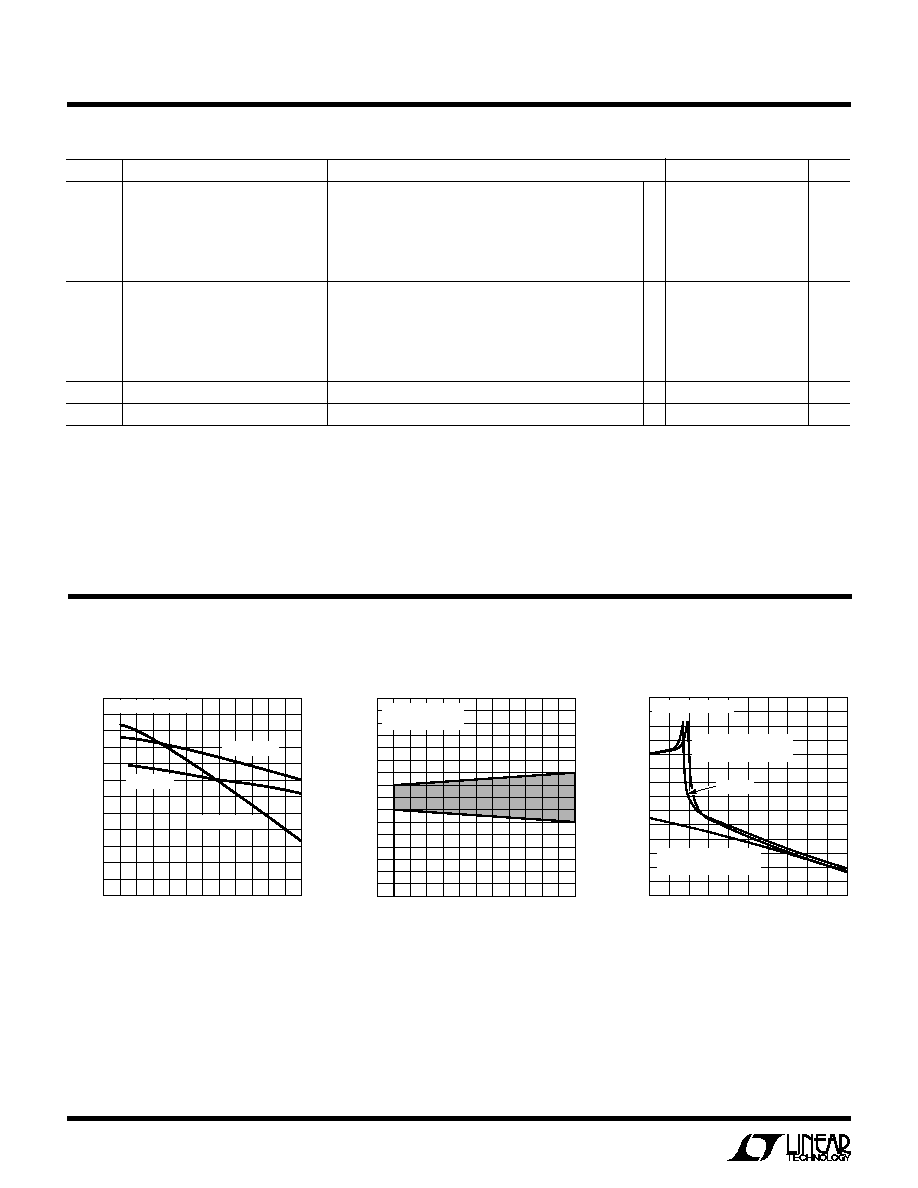
Efficiency vs Input Voltage
LOAD CURRENT (A)
0
50
V
OUT
(mV)
40
30
20
20
0
1
2
10
10
3
4
5
LTC1266 · TPC03
V
IN
= 5V
FIGURE 1 CIRCUIT
V
IN
= 9V (Burst Mode
OPERATION ENABLED)
V
IN
= 5V (Burst Mode
OPERATION INHIBITED)
Line Regulation
Load Regulation
INPUT VOLTAGE (V)
3
70
EFFICIENCY (%)
75
80
85
90
100
4
5
6
7
LTC1266 · TPC01
8
9
95
I
LOAD
= 2.5A
FIGURE 1 CIRCUIT
I
LOAD
= 5A
I
LOAD
= 100mA
C
C
HARA TERISTICS
U
W
A
TYPICAL PERFOR
CE
INPUT VOLTAGE (V)
3
V
OUT
(mV)
0
10
20
9
LTC1266 · TPC02
10
20
40
4
5
6
7
8
30
40
30
FIGURE 1 CIRCUIT
I
LOAD
= 1A
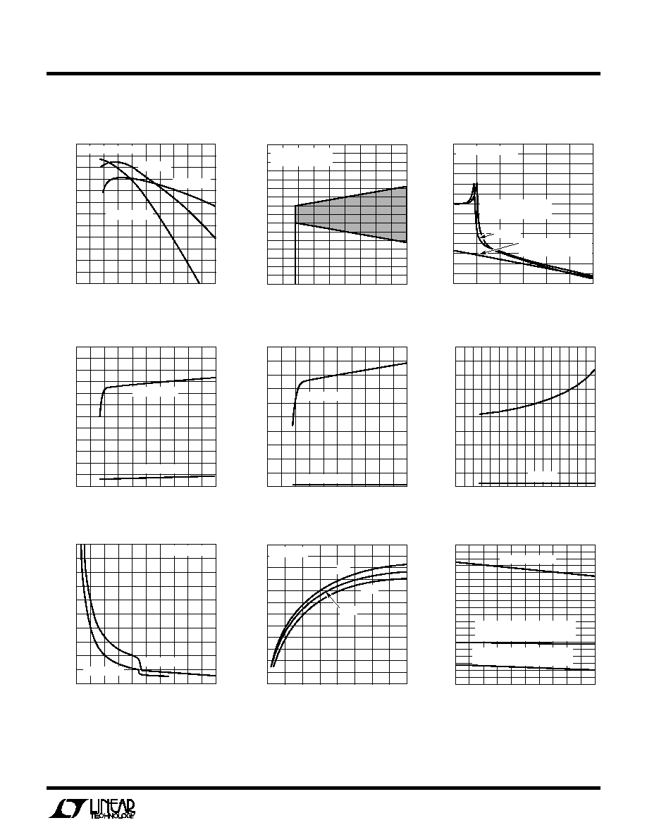
5
LTC1266
LTC1266-3.3/LTC1266-5
C
C
HARA TERISTICS
U
W
A
TYPICAL PERFOR
CE
INPUT VOLTAGE (V)
0
EFFICIENCY (%)
85
90
95
100
16
LTC1266 · TPC04
80
75
70
4
8
12
20
FIGURE 11 CIRCUIT
I
LOAD
= 2.5A
I
LOAD
= 100mA
I
LOAD
= 1A
LOAD CURRENT (A)
0
40
V
OUT
(mV)
30
20
10
30
10
0.5
1.0
20
0
1.5
2.0
2.5
3.0
LTC1266 · TPC06
FIGURE 11 CIRCUIT
V
IN
= 12V (Burst Mode
OPERATION ENABLED)
V
IN
= 5V
V
IN
= 5V (Burst Mode
OPERATION INHIBITED)
INPUT VOLTAGE (V)
0
SUPPLY CURRENT (mA)
1.5
2.0
2.5
3.0
16
LTC1266 · TPC07
1.0
0.5
0
4
8
12
20
ACTIVE MODE
SLEEP MODE
INPUT VOLTAGE (V)
0
SUPPLY CURRENT (
µ
A)
15
20
25
16
LTC1266 · TPC08
10
5
0
4
8
12
20
ACTIVE MODE
SLEEP MODE
INPUT VOLTAGE (V)
0
SUPPLY CURRENT (
µ
A)
30
40
50
LTC1266 · TPC09
20
10
0
5
10
15
20
V
IN
PWR V
IN
OUTPUT VOLTAGE (V)
0
1
OFF-TIME (
µ
s)
40
60
5
LTC1266 · TPC10
20
0
2
3
4
100
80
LTC1266-3.3
LTC1266-5
V
SENSE
= V
OUT
(V
IN
V
OUT
) VOLTAGE (V)
0
NORMALIZED FREQUENCY
2.5
3.0
12
10
8
LTC1266 · TPC11
0.5
1.5
2.0
1.0
0
2
4
6
14
16
V
OUT
= 3.3V
0
°
C
70
°
C
25
°
C
INPUT VOLTAGE (V)
0
V
OUT
(mV)
0
10
20
16
LTC1266 · TPC05
10
20
4
8
12
30
40
30
40
FIGURE 11 CIRCUIT
I
LOAD
= 1A
TEMPERATURE (
°
C)
0
SENSE VOLTAGE (mV)
100
150
200
80
LTC1266 · TPC12
50
0
50
20
40
60
100
MAX THRESHOLD
MIN THRESHOLD (Burst Mode
OPERATION INHIBIT)
MIN THRESHOLD (Burst Mode
OPERATION ENABLED)
Efficiency vs Input Voltage
V
IN
DC Supply Current
Off-Time vs Output Voltage
Line Regulation
Operating Frequency
vs (V
IN
V
OUT
) Voltage
Power V
IN
DC Supply Current
Load Regulation
Supply Current in Shutdown
Current Sense Threshold Voltage