 | –≠–ª–µ–∫—Ç—Ä–æ–Ω–Ω—ã–π –∫–æ–º–ø–æ–Ω–µ–Ω—Ç: LTC1276 | –°–∫–∞—á–∞—Ç—å:  PDF PDF  ZIP ZIP |

1
LTC1273
LTC1275/LTC1276
S
FEATURE
D
U
ESCRIPTIO
s
Single Supply 5V or
±
5V Operation
s
300ksps Sample Rate
s
75mW (Typ) Power Dissipation
s
On-Chip 25ppm/
∞
C Reference
s
Internal Synchronized Clock; No Clock Required
s
High Impedance Analog Input
s
70dB S/(N + D) and 77dB THD at Nyquist
s
±
1/2LSB INL and
±
3/4LSB DNL Max (A Grade)
s
ESD Protected On All Pins
s
24-Pin Narrow DIP and SOL Packages
s
Variety of Input Ranges:
0V to 5V (LTC1273)
±
2.5V (LTC1275)
±
5V (LTC1276)
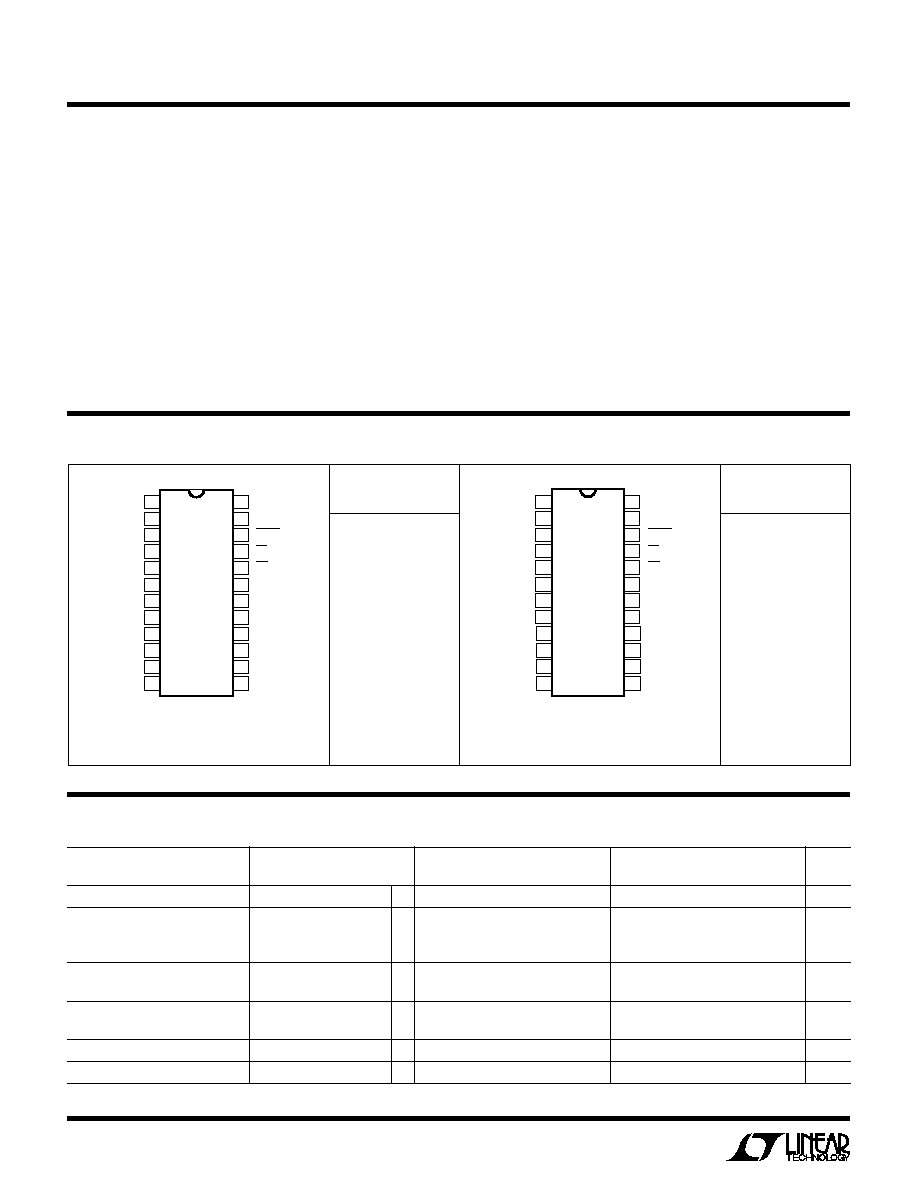
Effective Bits and Signal to (Noise + Distortion)
vs Input Frequency
LTBiCMOS
TM
is a trademark of Linear Technology Corporation
1
2
3
4
5
6
7
8
9
10
11
12
24
23
22
21
20
19
18
17
16
15
14
13
A
IN
V
REF
AGND
D11
D10
D9
D8
D7
D6
D5
D4
DGND
V
DD
NC
BUSY
CS
RD
HBEN
NC
NC
D0/8
D1/9
D2/10
D3/11
LTC1273
+
0.1
µ
F
10
µ
F
2.42V
V
REF
OUTPUT
ANALOG INPUT
(0V TO 5V)
+
10
µ
F
0.1
µ
F
5V
8- OR 12-BIT
PARALLEL BUS
µ
P CONTROL
LINES
LTC1273/75/76 ∑ TA01
INPUT FREQUENCY (Hz)
10k
0
EFFECTIVE BITS
3
5
7
10
100k
2M
LTC1273/75/76 ∑ TA02
1
4
6
9
12
11
8
2
1M
62
56
74
68
50
S/(N + D) (dB)
f
SAMPLE
= 300kHz
NYQUIST
FREQUENCY
U
S
A
O
PPLICATI
s
High Speed Data Acquisition
s
Digital Signal Processing
s
Multiplexed Data Acquisition Systems
s
Audio and Telecom Processing
s
Spectrum Analysis
The LTC1273/LTC1275/LTC1276 are 300ksps, sampling
12-bit A/D converters that draw only 75mW from single
5V or
±
5V supplies. These easy-to-use devices come
complete with 600ns sample-and-holds, precision refer-
ences and internally trimmed clocks. Unipolar and bipo-
lar conversion modes provide flexibility for various appli-
cations. They are built with LTBiCMOS
TM
switched ca-
pacitor technology.
These devices have 25ppm/
∞
C (max) internal references.
The LTC1273 converts 0V to 5V unipolar inputs from a
single 5V supply. The LTC1275/LTC1276 convert
±
2.5V
and
±
5V respectively from
±
5V supplies. Maximum DC
specifications include
±
1/2LSB INL,
±
3/4LSB DNL and
25ppm/
∞
C full scale drift over temperature. Outstanding
AC performance includes 70dB S/(N + D) and 77dB THD
at the Nyquist input frequency of 150kHz.
The internal clock is trimmed for 2.7
µ
s maximum conver-
sion time. The clock automatically synchronizes to each
sample command eliminating problems with asynchro-
nous clock noise found in competitive devices. A high
speed parallel interface eases connections to FIFOs, DSPs
and microprocessors.
12-Bit, 300ksps Sampling
A/D Converters with Reference
U
A
O
PPLICATI
TYPICAL
Single 5V Supply, 300ksps, 12-Bit Sampling A/D Converter
2
LTC1273
LTC1275/LTC1276
A
U
G
W
A
W
U
W
A
R
BSOLUTE
XI
TI
S
(Notes 1 and 2)
Supply Voltage (V
DD
) .............................................. 12V
Negative Supply Voltage (V
SS
)
LTC1275/LTC1276.................................. ≠ 6V to GND
Total Supply Voltage (V
DD
to V
SS
)
LTC1275/LTC1276............................................... 12V
Analog Input Voltage (Note 3)
LTC1273 .................................... ≠ 0.3V to V
DD
+ 0.3V
LTC1275/LTC1276.............. V
SS
≠ 0.3V to V
DD
+ 0.3V
Digital Input Voltage (Note 4)
LTC1273 ................................................ ≠ 0.3V to 12V
LTC1275/LTC1276......................... V
SS
≠ 0.3V to 12V
Digital Output Voltage (Note 3)
LTC1273 .................................... ≠ 0.3V to V
DD
+ 0.3V
LTC1275/LTC1276 .............. V
SS
≠ 0.3V to V
DD
+ 0.3V
Power Dissipation ............................................. 500mW
Operating Temperature Range
LTC1273AC, LTC1273BC, LTC1275AC
LTC1275BC, LTC1276AC, LTC1276BC .... 0
∞
C to 70
∞
C
Storage Temperature Range ................ ≠ 65
∞
C to 150
∞
C
Lead Temperature (Soldering, 10 sec) ................. 300
∞
C
W
U
U
PACKAGE/ORDER I FOR ATIO
ORDER
PART NUMBER
ORDER
PART NUMBER
1
2
3
4
5
6
7
8
9
10
11
12
TOP VIEW
S PACKAGE
24-LEAD PLASTIC SOL
24
23
22
21
20
19
18
17
16
15
14
13
A
IN
V
REF
AGND
D11
D10
D9
D8
D7
D6
D5
D4
DGND
V
DD
NC
BUSY
CS
RD
HBEN
NC
NC
D0/8
D1/9
D2/10
D3/11
N PACKAGE
24-LEAD PLASTIC DIP
1
2
3
4
5
6
7
8
9
10
11
12
TOP VIEW
S PACKAGE
24-LEAD PLASTIC SOL
24
23
22
21
20
19
18
17
16
15
14
13
A
IN
V
REF
AGND
D11
D10
D9
D8
D7
D6
D5
D4
DGND
V
DD
V
SS
BUSY
CS
RD
HBEN
NC
NC
D0/8
D1/9
D2/10
D3/11
N PACKAGE
24-LEAD PLASTIC DIP
T
JMAX
= 110
∞
C,
JA
= 100
∞
C/W (N)
T
JMAX
= 110
∞
C,
JA
= 130
∞
C/W (S)
T
JMAX
= 110
∞
C,
JA
= 100
∞
C/W (N)
T
JMAX
= 110
∞
C,
JA
= 130
∞
C/W (S)
With Internal Reference (Notes 5 and 6)
C
C
HARA TERISTICS
CO
U
VERTER
PARAMETER
CONDITIONS
MIN
TYP
MAX
MIN
TYP
MAX
UNITS
Resolution (No Missing Codes)
q
12
12
Bits
Integral Linearity Error
(Note 7)
±
1/2
±
1
LSB
Commercial
q
±
1/2
±
1
LSB
Military
q
±
3/4
±
1
LSB
Differential Linearity Error
Commercial
q
±
3/4
±
1
LSB
Military
q
±
1
±
1
LSB
Offset Error
(Note 8)
±
3
±
4
LSB
q
±
4
±
6
LSB
Full Scale Error
±
10
±
15
LSB
Full Scale Tempco
I
OUT(REFERENCE)
= 0
q
±
5
±
25
±
10
±
45
ppm/
∞
C
LTC1273A/LTC1275A/LTC1276A
LTC1273B/LTC1275B/LTC1276B
LTC1275ACN
LTC1275BCN
LTC1275ACS
LTC1275BCS
LTC1276ACN
LTC1276BCN
LTC1276ACS
LTC1276BCS
(For MIL Grade:
Contact Factory)
LTC1273ACN
LTC1273BCN
LTC1273ACS
LTC1273BCS
(For MIL Grade:
Contact Factory)

3
LTC1273
LTC1275/LTC1276
SYMBOL
PARAMETER
CONDITIONS
MIN
TYP
MAX
UNITS
S/(N + D) Signal-to-Noise Plus Distortion Ratio
50kHz/150kHz Input Signal
72/70
dB
THD
Total Harmonic Distortion
50kHz/150kHz Input Signal
≠ 83/≠ 74
dB
Up to 5th Harmonic
Peak Harmonic or Spurious Noise
50kHz/150kHz Input Signal
≠ 85/≠ 76
dB
IMD
Intermodulation Distortion
f
IN1
= 29.37kHz, f
IN2
= 32.446kHz
≠ 80
dB
Full Power Bandwidth
4.5
MHz
Full Linear Bandwidth (S/(N + D)
68dB)
200
kHz
SYMBOL
PARAMETER
CONDITIONS
MIN
TYP
MAX
UNITS
V
IN
Analog Input Range (Note 9)
4.95V
V
DD
5.25V (LTC1273)
q
0 to 5
V
4.75V
V
DD
5.25V, ≠ 5.25V
V
SS
≠ 2.45V (LTC1275)
q
±
2.5
V
4.95V
V
DD
5.25V, ≠ 5.25V
V
SS
≠ 4.95V (LTC1276)
q
±
5
V
I
IN
Analog Input Leakage Current
CS = High
q
±
1
µ
A
C
IN
Analog Input Capacitance
Between Conversions (Sample Mode)
50
pF
During Conversions (Hold Mode)
5
pF
t
ACQ
Sample-and-Hold
Commercial
q
600
ns
Acquisition Time
Military
q
1000
ns
(Note 5)
ACCURACY
IC
DY
U
W
A
(Note 5)
LTC1273A/LTC1275A/LTC1276A
LTC1273B/LTC1275B/LTC1276B
PUT
U
I
A
A
U
LOG
LTC1273A/LTC1275A/LTC1276A
LTC1273B/LTC1275B/LTC1276B
PARAMETER
CONDITIONS
MIN
TYP
MAX
MIN
TYP
MAX
UNITS
V
REF
Output Voltage
I
OUT
= 0
2.400
2.420
2.440
2.400
2.420
2.440
V
V
REF
Output Tempco
I
OUT
= 0
q
±
5
±
25
±
10
±
45
ppm/
∞
C
V
REF
Line Regulation
4.95V
V
DD
5.25V
0.01
0.01
LSB/V
≠ 5.25V
V
SS
≠ 4.95V
0.01
0.01
LSB/V
V
REF
Load Regulation
0V
|
I
OUT
|
1mA
2
2
LSB/mA
LTC1273B/LTC1275B/LTC1276B
LTC1273A/LTC1275A/LTC1276A
DIGITAL I PUTS A D DIGITAL OUTPUTS
U
U
LTC1273A/LTC1275A/LTC1276A
LTC1273B/LTC1275B/LTC1276B
SYMBOL
PARAMETER
CONDITIONS
MIN
TYP
MAX
UNITS
V
IH
High Level Input Voltage
V
DD
= 5.25V
q
2.4
V
V
IL
Low Level Input Voltage
V
DD
= 4.95V
q
0.8
V
I
IN
Digital Input Current
V
IN
= 0V to V
DD
q
±
10
µ
A
C
IN
Digital Input Capacitance
5
pF
V
OH
High Level Output Voltage
V
DD
= 4.95V
I
O
= ≠ 10
µ
A
4.7
V
I
O
= ≠ 200
µ
A
q
4.0
V
(Note 5)
I TER AL REFERE CE CHARACTERISTICS
(Note 5)
U
U
U
4
LTC1273
LTC1275/LTC1276
SYMBOL
PARAMETER
CONDITIONS
MIN
TYP
MAX
UNITS
f
SAMPLE(MAX)
Maximum Sampling Frequency
(Note 10)
Commercial
q
300
kHz
Military
q
250
kHz
t
CONV
Conversion Time
Commercial
q
2.7
µ
s
Military
q
3.0
µ
s
t
1
CS to RD Setup Time
q
0
ns
t
2
RD to BUSY Delay
C
L
= 50pF
80
190
ns
Commercial
q
230
ns
Military
q
270
ns
t
3
Data Access Time After RD
C
L
= 20pF
40
90
ns
Commercial
q
110
ns
Military
q
120
ns
C
L
= 100pF
50
125
ns
Commercial
q
150
ns
Military
q
170
ns
t
4
RD Pulse Width
q
t
3
ns
t
5
CS to RD Hold Time
q
0
ns
t
6
Data Setup Time After BUSY
40
70
ns
Commercial
q
90
ns
Military
q
100
ns
DIGITAL I PUTS A D DIGITAL OUTPUTS
U
U
LTC1273A/LTC1275A/LTC1276A
LTC1273B/LTC1275B/LTC1276B
SYMBOL
PARAMETER
CONDITIONS
MIN
TYP
MAX
UNITS
V
OL
Low Level Output Voltage
V
DD
= 4.95V
I
O
= 160
µ
A
0.05
V
I
O
= 1.6mA
q
0.10
0.4
V
I
OZ
High Z Output Leakage D11-D0/8
V
OUT
= 0V to V
DD
, CS High
q
±
10
µ
A
C
OZ
High Z Output Capacitance D11-D0/8
CS High (Note 9 )
q
15
pF
I
SOURCE
Output Source Current
V
OUT
= 0V
≠ 10
mA
I
SINK
Output Sink Current
V
OUT
= V
DD
10
mA
(Note 5)
LTC1273A/LTC1275A/LTC1276A
LTC1273B/LTC1275B/LTC1276B
SYMBOL
PARAMETER
CONDITIONS
MIN
TYP
MAX
UNITS
V
DD
Positive Supply Voltage
LTC1273/LTC1276 (Notes 10, 11)
4.95
5.25
V
LTC1275 (Note 10)
4.75
5.25
V
V
SS
Negative Supply Voltage
LTC1275 (Note 10)
≠ 2.45
≠ 5.25
V
LTC1276 (Notes 10, 11)
≠ 4.95
≠ 5.25
V
I
DD
Positive Supply Current
q
15
25
mA
I
SS
Negative Supply Current
LTC1275/LTC1276
q
0.065
0.200
mA
P
D
Power Dissipation
75
mW
TI I G CHARACTERISTICS
W U
POWER REQUIRE E TS
W U
LTC1273A/LTC1275A/LTC1276A
LTC1273B/LTC1275B/LTC1276B
(Note 5)
See Timing Characteristics Figures (Note 5)

5
LTC1273
LTC1275/LTC1276
SYMBOL
PARAMETER
CONDITIONS
MIN
TYP
MAX
UNITS
t
7
Bus Relinquish Time
20
30
75
ns
Commercial
q
20
85
ns
Military
q
20
90
ns
t
8
HBEN to RD Setup Time
q
0
ns
t
9
HBEN to RD Hold Time
q
0
ns
t
10
Delay Between RD Operations
q
40
ns
t
11
Delay Between Conversions
(Note 10)
500
ns
Commercial
q
600
ns
Military
q
1000
ns
t
12
Aperture Delay of Sample-and-Hold
25
ns
TI I G CHARACTERISTICS
W U
LTC1273A/LTC1275A/LTC1276A
LTC1273B/LTC1275B/LTC1276B
See Timing Characteristics Figures (Note 5)
Note 6: Linearity, offset and full scale specifications apply for unipolar and
bipolar modes.
Note 7: Integral nonlinearity is defined as the deviation of a code from a
straight line passing through the actual endpoints of the transfer curve.
The deviation is measured from the center of the quantization band.
Note 8: Bipolar offset (LTC1275/LTC1276) is the different voltage
measured from ≠ 0.5LSB when the LTC1275/LTC1276 output code flickers
between 0000 0000 0000 and 1111 1111 1111.
Note 9: Guaranteed by design, not subject to test.
Note 10: Recommended operating conditions.
Note11: A
IN
must not exceed V
DD
or fall below V
SS
by more than 50mV for
specified accuracy. Therefore the minimum supply voltage for the
LTC1273 is + 4.95V. The minimum supplies for the LTC1275 are +4.75V
and ≠ 2.45V and the minimum supplies for the LTC1276 are
±
4.95V.
The
q
indicates specifications which apply over the full operating
temperature range; all other limits and typicals T
A
= 25
∞
C.
Note 1: Absolute maximum ratings are those values beyond which the life
of a device may be impaired.
Note 2: All voltage values are with respect to ground with DGND and
AGND wired together (unless otherwise noted).
Note 3: When these pin voltages are taken below V
SS
(ground for
LTC1273) or above V
DD
, they will be clamped by internal diodes. This
product can handle input currents greater than 60mA below V
SS
(ground
for LTC1273) or above V
DD
without latch-up.
Note 4: When these pin voltages are taken below V
SS
(ground for
LTC1273) they will be clamped by internal diodes. This product can handle
input currents greater than 60mA below V
SS
(ground for LTC1273)
without latch-up. These pins are not clamped to V
DD
.
Note 5: V
DD
= 5V (V
SS
= ≠ 5V for LTC1275/LTC1276), 300kHz at 70
∞
C and
250kHz at 125
∞
C, t
r
= t
f
= 5ns unless otherwise specified.
TI I G CHARACTERISTICS
(Note 5)
W U
Slow Memory Mode, Parallel Read Timing Diagram
ROM Mode, Parallel Read Timing Diagram
BUSY
DATA
TRACK
OLD DATA
DB11 TO DB0
NEW DATA
DB11 TO DB0
t
1
HOLD
LTC1273/75/76 ∑ TA03
CS
RD
t
5
t
1
t
10
t
11
t
2
t
CONV
t
6
t
3
t
12
t
7
t
1
OLD DATA
DB11 TO DB0
NEW DATA
DB11 TO DB0
DATA
TRACK
HOLD
CS
RD
BUSY
LTC1273/75/76 ∑ TA04
t
5
t
1
t
5
t
4
t
2
t
CONV
t
11
t
2
t
CONV
t
3
t
7
t
3
t
12
t
12
t
4
t
7