 | –≠–ª–µ–∫—Ç—Ä–æ–Ω–Ω—ã–π –∫–æ–º–ø–æ–Ω–µ–Ω—Ç: LTC1314 | –°–∫–∞—á–∞—Ç—å:  PDF PDF  ZIP ZIP |

1
LTC1314/LTC1315
PCMCIA Switching Matrix
with Built-In N-Channel
V
CC
Switch Drivers
S
FEATURE
D
U
ESCRIPTIO
s
Output Current Capability: 120mA
s
External 12V Regulator Can Be Shut Down
s
Built-In N-Channel V
CC
Switch Drivers
s
Digital Selection of 0V, V
CCIN
, VPP
IN
or Hi-Z
s
3.3V or 5V V
CC
Supply
s
Break-Before-Make Switching
s
0.1
µ
A Quiescent Current in Hi-Z or 0V Mode
s
No VPP
OUT
Overshoot
s
Logic Compatible with Standard PCMCIA Controllers
The LTC
Æ
1314/LTC1315 provide the power switching
necessary to control Personal Computer Memory Card
International Association (PCMCIA) Release 2.0 card slots.
When used in conjunction with a PC card interface control-
ler, these devices form a complete minimum component
count interface for palmtop, pen-based and notebook
computers.
The LTC1314/LTC1315 provide 0V, 3.3V, 5V, 12V and
Hi-Z power output for flash VPP programming. A built-in
charge pump produces 12V of gate drive for inexpensive
N-channel 3.3V/5V V
CC
switching. The 12V regulator can
be shut down when 12V is not required at VPP
OUT
. All
digital inputs are TTL compatible and interface directly
with industry standard PC card interface controllers.
The LTC1314 is available in 14-pin SO and the LTC1315 in
24-pin SSOP.
s
Notebook Computers
s
Palmtop Computers
s
Pen-Based Computers
s
Handi-Terminals
s
Bar-Code Readers
U
S
A
O
PPLICATI
, LTC and LT are registered trademarks of Linear Technology Corporation.
TYPICAL APPLICATIO
N
U
Linear Technology PCMCIA Product Family
DEVICE
DESCRIPTION
PACKAGE
LT1312
SINGLE PCMCIA VPP DRIVER/REGULATOR
8-PIN SO
LT1313
DUAL PCMCIA VPP DRIVER/REGULATOR
16-PIN SO*
LTC
Æ
1314
SINGLE PCMCIA SWITCH MATRIX
14-PIN SO
LTC1315
DUAL PCMCIA SWITCH MATRIX
24-PIN SSOP
LTC1470
PROTECTED V
CC
5V/3.3V SWITCH MATRIX
8-PIN SO
LTC1472
PROTECTED V
CC
AND VPP SWITCH MATRIX
16-PIN SO*
*NARROW BODY
EN0
EN1
V
CC0
V
CC1
VPP
OUT
DRV3
DRV5
0
0
X
X
GND
X
X
0
1
X
X
V
CCIN
X
X
1
0
X
X
VPP
IN
X
X
1
1
X
X
Hi-Z
X
X
X
X
1
0
X
1
0
X
X
0
1
X
0
1
X
X
0
0
X
0
0
X
X
1
1
X
0
0
X = DON'T CARE
LTC1314 Truth Table
Typical PCMCIA Single Slot Driver
+
VPP
IN
C
OUT
SHDN
3.3V OR 5V
V
DD
VPP
OUT
VPP1
VPP2
V
CC
LTC1314 ∑ TA01
LTC1314
5V
12V
PCMCIA
CARD SLOT
CONTROLLER
EN0
EN1
V
CC0
V
CC1
DRV5
V
CCIN
DRV3
GND
5V
3.3V
PCMCIA
CARD SLOT
+
1
µ
F
0.1
µ
F
STEP-UP
REGULATOR
LT
Æ
1301
V
IN
V
OUT
SHDN

2
LTC1314/LTC1315
A
U
G
W
A
W
U
W
A
R
BSOLUTE
XI
TI
S
VPP
IN
to GND ........................................ 13.2V to ≠ 0.3V
V
DD
to GND ................................................. 7V to ≠ 0.3V
V
CCIN
to GND .............................................. 7V to ≠ 0.3V
VPP
OUT
to GND...................................... 13.2V to ≠ 0.3V
Digital Input Voltage ................................... 7V to ≠ 0.3V
Operating Temperature Range .................... 0
∞
C to 70
∞
C
Storage Temperature Range ................ ≠ 65
∞
C to 150
∞
C
Lead Temperature (Soldering, 10 sec)................. 300
∞
C
W
U
U
PACKAGE/ORDER I FOR ATIO
ELECTRICAL CHARACTERISTICS
LTC1314/LTC1315
SYMBOL
PARAMETER
CONDITIONS
MIN
TYP
MAX
UNITS
V
CCIN
Input Voltage Range
q
3
5.5
V
VPP
IN
Input Voltage Range
q
0
12.6
V
V
DD
Supply Voltage Range
q
4.5
5.5
V
I
CC
V
CCIN
Supply Current, No Load
VPP
OUT
= VPP
IN
, V
CCIN
, 0V or Hi-Z
q
0.1
1
µ
A
I
PP
VPP
IN
Supply Current, No Load
VPP
OUT
= VPP
IN
, V
CCIN
q
15
40
µ
A
VPP
OUT
= 0V, Hi-Z
q
0.1
1
µ
A
I
DD
V
DD
Supply Current, No Load
VPP
OUT
= VPP
IN
or V
CCIN
q
60
120
µ
A
VPP
OUT
= 0V or Hi-Z
q
0.1
10
µ
A
VPP
OUT
= 0V or Hi-Z, DRV3 or DRV5 On
q
85
200
µ
A
I
IN
Input Current: EN0, EN1, V
CC0
or V
CC1
0V < V
IN
< V
DD
q
±
1
µ
A
I
OUT
High Impedance Output Leakage Current
EN0 = EN1 = 5V, 0V < VPP
OUT
< 12V
q
0.1
10
µ
A
R
ON
On Resistance, VPP
OUT
= VPP
IN
VPP
IN
= 12V, I
LOAD
= 120mA
q
0.55
1.2
On Resistance, VPP
OUT
= V
CCIN
V
CCIN
= 5V, I
LOAD
= 5mA
q
2
5
On Resistance, VPP
OUT
= GND
V
DD
= 5V, I
SINK
= 1mA
q
100
250
V
INH
Input High Voltage, Digital Inputs
q
2
V
V
INL
Input Low Voltage, Digital Inputs
q
0.8
V
V
DD
= 5V, V
CCIN
= 5V, VPP
IN
= 12V, T
A
= 25
∞
C unless otherwise specified.
LTC1314CS
ORDER PART
NUMBER
ORDER PART
NUMBER
1
2
3
4
5
6
7
8
9
10
11
12
TOP VIEW
G PACKAGE
24-LEAD PLASTIC SSOP
24
23
22
21
20
19
18
17
16
15
14
13
AVPP
IN
ASHDN
AEN0
AEN1
AV
CC0
AV
CC1
BVPP
IN
BSHDN
BEN0
BEN1
BV
CC0
BV
CC1
AV
CCIN
AVPP
OUT
GND
V
DD
ADRV3
ADRV5
BV
CCIN
BVPP
OUT
GND
V
DD
BDRV3
BDRV5
T
JMAX
= 125
∞
C,
JA
= 95
∞
C/W
T
JMAX
= 125
∞
C,
JA
= 110
∞
C/W
Consult factory for Industrial and Military grade parts.
LTC1315CG
TOP VIEW
S PACKAGE
14-LEAD PLASTIC SO
1
2
3
4
5
6
7
14
13
12
11
10
9
8
VPP
IN
NC
SHDN
EN0
EN1
V
CC0
V
CC1
V
CCIN
NC
VPP
OUT
GND
V
DD
DRV3
DRV5

3
LTC1314/LTC1315
ELECTRICAL CHARACTERISTICS
V
DD
= 5V, V
CCIN
= 5V, VPP
IN
= 12V, T
A
= 25
∞
C unless otherwise specified.
LTC1314/LTC1315
SYMBOL
PARAMETER
CONDITIONS
MIN
TYP
MAX
UNITS
V
OH
SHDN Output High Voltage
VPP
OUT
= V
CCIN
, 0V or Hi-Z, I
LOAD
= 400
µ
A
q
3.5
V
V
OL
SHDN Output Low Voltage
VPP
OUT
= VPP
IN
, I
SINK
= 400
µ
A
q
0.4
V
V
G
-V
DD
Gate Voltage Above Supply
V
DRV3
or V
DRV5
q
6
7
13
V
t
ON
Turn-On Time, DRV3 and DRV5
C
GATE
= 1000pF, Time for V
GATE
> V
DD
+ 1V
50
150
500
µ
s
t
OFF
Turn-Off Time, DRV3 and DRV5
C
GATE
= 1000pF, Time for V
GATE
< 0.5V
3
10
30
µ
s
t
1
Delay + Rise Time
VPP
OUT
= GND to V
CCIN
, VPP
IN
= 0V, Note 1
5
15
50
µ
s
t
2
Delay + Rise Time
VPP
OUT
= GND to VPP
IN
(Note 1)
5
15
50
µ
s
t
3
Delay + Rise Time
VPP
OUT
= V
CCIN
to VPP
IN
(Note 1)
5
15
50
µ
s
t
4
Delay + Fall Time
VPP
OUT
= VPP
IN
to V
CCIN
(Note 3)
2
6
20
µ
s
t
5
Delay + Fall Time
VPP
OUT
= VPP
IN
to GND (Note 2)
15
50
150
µ
s
t
6
Delay + Fall Time
VPP
OUT
= V
CCIN
to GND, VPP
IN
= 0V (Note 2)
10
25
100
µ
s
t
7
Output Turn-On Delay
VPP
OUT
= Hi-Z to VPP
IN
or V
CCIN
(Notes 1, 6)
5
15
50
µ
s
TYPICAL PERFOR
M
A
N
CE CHARACTERISTICS
U
W
TEMPERATURE (
∞
C)
≠50
SWITCH ON RESISTANCE (
)
3.0
2.7
2.4
2.1
1.8
1.5
1.2
0.9
0.6
0.3
0
≠10
30
50
1314/15 G01
≠30
10
70
90
V
CC
SWITCH
VPP SWITCH
Switch On Resistance vs
Temperature
TEMPERATURE (
∞
C)
≠50
DRV3/DRV5 OUTPUT VOLTAGE (V)
14.2
14.0
13.8
13.6
13.4
13.2
13.0
10
50
1314/15 G03
≠30
≠10
30
70
90
Supply Current vs Temperature
DRV3/DRV5 Output Voltage vs
Temperature
TEMPERATURE (
∞
C)
≠50
SUPPLY CURRENT (
µ
A)
75
70
65
60
55
50
45
40
35
30
25
≠10
30
50
1314/15 G02
≠30
10
70
90
VPP
OUT
= VPP
IN
= 12V
VPP
OUT
= V
CCIN
VPP
IN
= 12V
The
q
denotes specifications which apply over the full operating
temperature range.
Note 1: To 90% of the final value, C
OUT
= 0.1
µ
F, R
OUT
= 2.9k.
Note 2: To 10% of the final value, C
OUT
= 0.1
µ
F, R
OUT
= 2.9k.
Note 3: To 50% of the initial value, C
OUT
= 0.1
µ
F, R
OUT
= 2.9k.
Note 4: Measured current data is per channel.
Note 5: Input logic low equal to 0V, high equal to 5V.
Note 6: VPP
IN
= 0V when switching from Hi-Z to V
CCIN
.

4
LTC1314/LTC1315
PI
N
FU
N
CTIO
N
S
U
U
U
TYPICAL PERFOR
M
A
N
CE CHARACTERISTICS
U
W
V
DD
(V)
0
1
I
DD
(
µ
A)
2
4
3
5
6
1314/15 G04
80
70
60
50
40
30
20
10
0
VPP
OUT
= VPP
IN
VPP
OUT
= V
CCIN
VPP
OUT
= 0V
OR HI-Z
VPP
IN
= 12V
V
CCIN
= 5V
T = 25
∞
C
VPP
IN
(V)
0
IPP
IN
(
µ
A)
20
18
16
14
12
10
8
6
4
2
0
4
8
10
1314/15 G05
2
6
12
14
VPP
OUT
= VPP
IN
VPP
OUT
= V
CCIN
VPP
OUT
= 0V
OR HI-Z
V
DD
= V
CCIN
= 5V
T = 25
∞
C
IPP
IN
vs VPP
IN
LTC1314
VPP
IN
(Pin 1): 12V Power Input.
NC (Pin 2): Not Connected.
SHDN (Pin 3): Shutdown Output. When the output is high,
the external 12V regulator can be shut down to conserve
power consumption.
EN0, EN1 (Pins 4, 5): Logic inputs that control the voltage
output on VPP
OUT
. The input thresholds are compatible
with TTL/CMOS levels. Refer to Truth Table.
V
CC0
(Pin 6): Logic input that controls the state of the
MOSFET gate driver DRV3. ESD protection device limits
input excursions to 0.6V below ground.
V
CC1
(Pin 7): Logic input that controls the state of the
MOSFET gate driver DRV5. ESD protection device limits
input excursions to 0.6V below ground.
DRV5, DRV3 (Pins 8, 9): Gate driver outputs that control
the external MOSFETs that switch the V
CC
pin of card slot
to Hi-Z, 3.3V, or 5V.
V
DD
(Pin 10): Positive Supply, 4.5V
V
DD
5.5V. This pin
supplies the power to the control logic and the charge
pumps and must be continuously powered.
GND (Pin 11): Ground Connection.
VPP
OUT
(Pin 12): Switched output that provides 0V, 3.3V,
5V, 12V, or Hi-Z to the VPP pin of the card slot. Refer to
Truth Table.
NC (Pin 13): Not Connected.
V
CCIN
(Pin 14): 5V or 3.3V Power Input.
I
DD
vs V
DD
5
LTC1314/LTC1315
PI
N
FU
N
CTIO
N
S
U
U
U
LTC1315
VPP
IN
(Pins 1, 7): 12V Power Inputs.
SHDN (Pins 2, 8): Shutdown Outputs. When the output is
high, the external 12V regulator can be shut down to
conserve power consumption.
EN0, EN1 (Pins 3, 4, 9, 10): Logic inputs that control the
voltage output on VPP
OUT
. The input thresholds are
compatible with TTL/CMOS levels. Refer to the Truth
Table.
V
CC0
(Pins 5, 11): Logic inputs that control the state of the
MOSFET gate driver DRV3. ESD protection device limits
input excursions to 0.6V below ground.
V
CC1
(Pins 6, 12): Logic inputs that control the state of the
MOSFET gate driver DRV5. ESD protection device limits
input excursions to 0.6V below ground.
DRV5, DRV3 (Pins 13, 14, 19, 20): Gate driver outputs
that control the external MOSFETs that switch the V
CC
pin
of card slot to Hi-Z, 3.3V, or 5V.
V
DD
(Pins 15, 21): Positive Supplies, 4.5V
V
DD
5.5V.
These pins supply the power to the control logic and the
charge pumps and must be continuously powered.
GND (Pins 16, 22): Ground Connections.
VPP
OUT
(Pins 17, 23): Switched outputs that provide 0V,
3.3V, 5V, 12V, or Hi-Z to the VPP pin of the card slot. Refer
to the Truth Table.
V
CCIN
(Pins 18, 24): 5V or 3.3V Power Inputs.
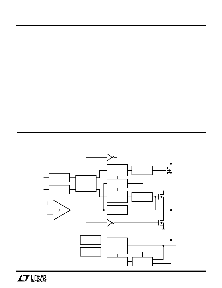
GATE CHARGE
AND DISCHARGE
CONTROL LOGIC
OSCILLATOR
AND BIAS
CHARGE
PUMP
CHARGE
PUMP
BREAK-BEFORE-
MAKE SWITCHES
TTL TO CMOS
CONVERTER
TTL TO CMOS
CONVERTER
GATE CHARGE
AND DISCHARGE
CONTROL LOGIC
GATE CHARGE
CONTROL LOGIC
OSCILLATOR AND
CHARGE PUMP
OUTPUT
SWITCHES
TTL TO CMOS
CONVERTER
TTL TO CMOS
CONVERTER
≠
+
SHDN
VPP
IN
VPP
IN
V
CC0
V
CC1
10V
EN1
EN0
V
CCIN
VPP
OUT
GND
DRV3
DRV5
LTC1314 ∑ BD
GATE CHARGE
AND DISCHARGE
CONTROL LOGIC
BLOCK DIAGRA
M
W
LTC1314 or 1/2 LTC1315

6
LTC1314/LTC1315
EN0
EN1
VPP
IN
VCC
IN
VPP
OUT
GND
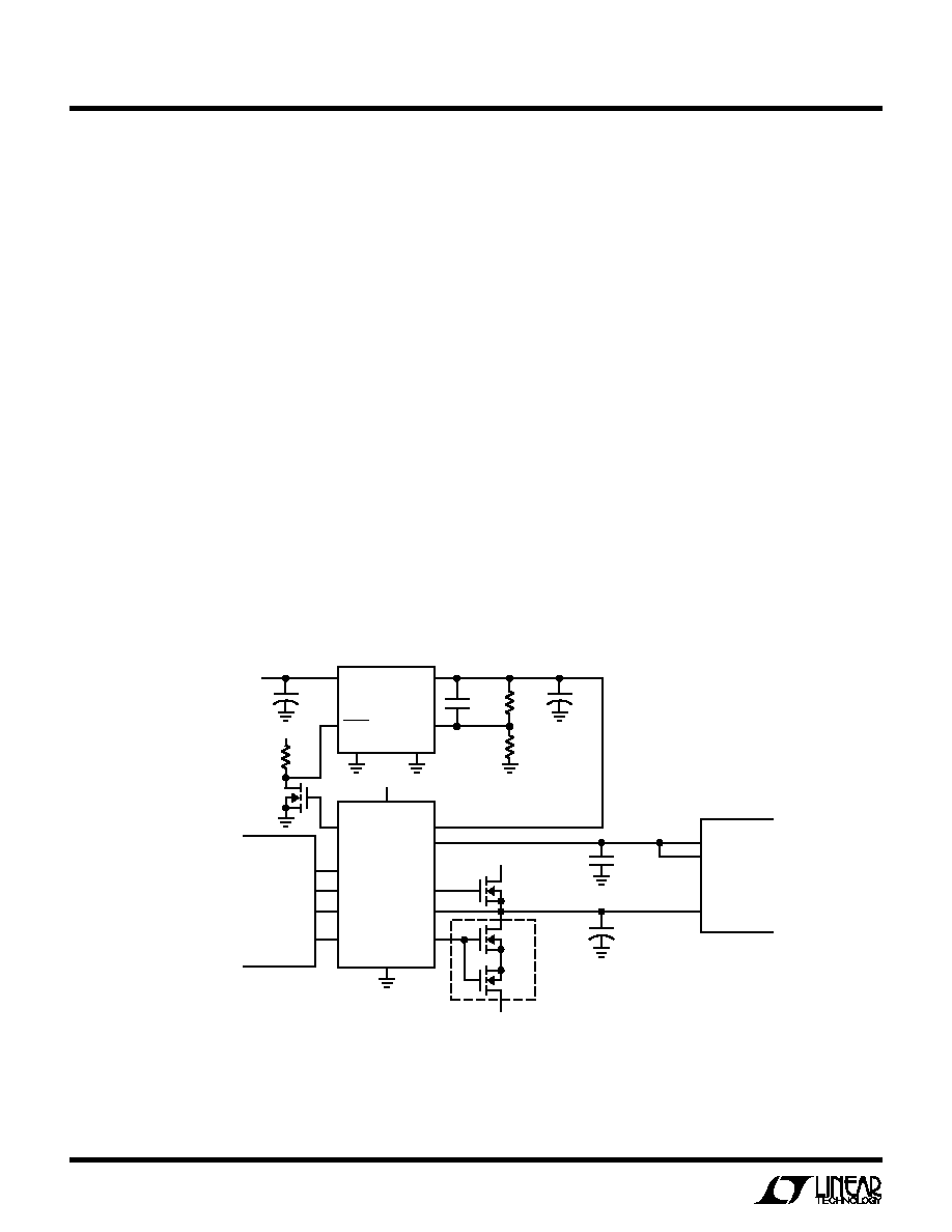
NOTE: 1
µ
F CAPACITOR CONNECTED ON BOTH VPP
IN
AND V
CCIN
PINS AT TIMING TEST
t
7
LTC1314 ∑ SW
t
5
t
2
t
4
t
1
t
6
t
3
Hi-Z
APPLICATIO
N
S I
N
FOR
M
ATIO
N
W
U
U
U
PCMCIA VPP control is easily accomplished using the
LTC1314 or LTC1315 switching matrix. Two control bits
(LTC1314) or four control bits (LTC1315) determine the
output voltage and standby/operate mode conditions. Out-
put voltages of 0V, V
CCIN
(3.3V or 5V), VPP
IN
, or a high
impedance state are available. When either the high imped-
ance or low voltage (0V) conditions are selected, the device
switches into "sleep" mode and draws 0.1
µ
A of current
from the V
DD
supply.
The LTC1314/LTC1315 are low resistance power MOSFET
switching matrices that operate from the computer system
main power supply. Device power is obtained from V
DD
,
which is 5V
±
0.5V. The gate drives for the NFETs (both
internal and external) are derived from internal charge
pumps, therefore VPP
IN
is only required when it's switched
to VPP
OUT
. Internal break-before-make switches deter-
mine the output voltage and device mode.
Flash Memory Card VPP Power Considerations
PCMCIA compatible flash memory cards require tight
regulation of the 12V VPP programming supply to ensure
that the internal flash memory circuits are never subjected
to damaging conditions. Flash memory circuits are typi-
cally rated with an absolute maximum of 13.5V and VPP
must be maintained at 12V
±
5% under all possible load
conditions during erase and program cycles. Undervoltage
can decrease specified flash memory reliability and over-
voltage can damage the device.
V
CC
Switch Driver and VPP Switch Matrix
Figures 1 and 2 show the approach that is very space and
power efficient. The LTC1314/LTC1315 used in conjunc-
tion with the LT1301 DC/DC converter, provide complete
power management for a PCMCIA card slot. The LTC1314/
LTC1315 and LT1301 combination provides a highly effi-
cient, minimal parts count solution. These circuits are
especially good for applications that are adding a PCMCIA
socket to existing systems that currently have only 5V or
3.3V available.
The LTC1314 drives three N-channel (LTC1315 six
N-channel) MOSFETs that provide V
CC
pin power switch-
ing. On-chip charge pumps provide the necessary voltage
to fully enhance the switches. With the charge pumps on-
chip, the MOSFET drive is available without the need for a
12V supply. The LTC1314/LTC1315 provide a natural
break-before-make action and smooth transitions due to
SWITCHI G TI E WAVEFOR S
U
W
W

7
LTC1314/LTC1315
APPLICATIO
N
S I
N
FOR
M
ATIO
N
W
U
U
U
Figure 1. LTC1314 Switch Matrix with the LT1301 Boost Regulator
Figure 2. Typical Two-Socket Application Using the LTC1315 and the LT1301
+
V
DD
C2
33
µ
F
AVPP
IN
ASHDN
BSHDN
Q1A
1/2 Si9956DY
Si9956DY
Q2A
Q2B
AVPP
OUT
BVPP
IN
VPP1
VPP2
V
CC
LTC1315
PCMCIA
CONTROLLER
AEN0
AEN1
SW
L1
22
µ
H
D1
MBRS130LT3
V
CC
GND
PGND
SENSE
SELECT
LT1301
SHDN
NC
C1: AVX TPSD476M016R0150
C2: AVX TPSD336M020R0200
L1: SUMIDA CD75-220K
I
LIM
AV
CC0
AV
CC1
ADRV5
AV
CCIN
ADRV3
GND
5V
3.3V
PC CARD
SOCKET
#1
+
C1
47
µ
F
+
1
µ
F
0.1
µ
F
Q1B
1/2 Si9956DY
Si9956DY
Q3A
Q3B
BVPP
OUT
VPP1
VPP2
V
CC
1314/15 F02
BEN0
BEN1
BV
CC0
BV
CC1
BDRV5
BV
CCIN
BDRV3
5V
3.3V
PC CARD
SOCKET
#2
+
1
µ
F
0.1
µ
F
+
V
DD
C2
33
µ
F
VPP
IN
SHDN
Q1A
1/2 Si9956DY
Si9956DY
Q2A
Q2B
VPP
OUT
VPP1
VPP2
V
CC
LTC1314 ∑ F01
LTC1314
PCMCIA
CONTROLLER
EN0
EN1
SW
L1
22
µ
H
D1
MBRS130LT3
V
CC
GND
PGND
SENSE
SELECT
LT1301
SHDN
NC
C1: AVX TPSD476M016R0150
C2: AVX TPSD336M020R0200
L1: SUMIDA CD75-220K
5V
I
LIM
V
CC0
V
CC1
DRV5
V
CCIN
DRV3
GND
5V
3.3V
PC CARD
SOCKET
+
C1
47
µ
F
+
1
µ
F
0.1
µ
F
8
LTC1314/LTC1315
APPLICATIO
N
S I
N
FOR
M
ATIO
N
W
U
U
U
+
V
DD
1
µ
F
VPP
IN
SHDN
Q1A
1/2 Si9956DY
Si9956DY
Q2A
Q2B
VPP
OUT
VPP1
VPP2
V
CC
1314/15 F03
LTC1314
PCMCIA
CONTROLLER
EN0
EN1
GND
PGND
V
OUT
2N7002
13V TO 20V
(MAY BE FROM
AUXILLARY
WINDING)
V
IN
200pF
121k
1%
56.2k
1%
LT1121
SHDN
5V
5V
ADJ
V
CC0
V
CC1
DRV5
V
CCIN
DRV3
GND
5V
3.3V
PC CARD
SOCKET
+
1
µ
F
0.1
µ
F
+
10
µ
F
100k
the asymmetrical turn-on and turn-off of the MOSFETs.
The LT1301 switching regulator is in shutdown mode and
consumes only 10
µ
A until the VPP pins require 12V.
The VPP switching is accomplished by a combination of
the LTC1314/LTC1315 and LT1301. The LT1301 is in
shutdown mode to conserve power until the VPP pins
require 12V. When the VPP pins require 12V, the LT1301
is activated and the LTC1314/LTC1315's internal switches
route the VPP
IN
pin to the VPP
OUT
pin. The LT1301 is
capable of delivering 12V at 120mA maintaining high
efficiency. The LTC1314/LTC1315's break-before-make
and slope-controlled switching will ensure that the output
voltage transition will be smooth, of moderate slope, and
without overshoot. This is critical for flash memory prod-
ucts to prevent damaging parts from overshoot and
ringing exceeding the 13.5V device limit.
With Higher Voltage Supplies Available
Often systems have an available supply voltage greater
than 12V. The LTC1314/LTC1315 can be used in conjunc-
tion with an LT1121 linear regulator to supply the PC card
socket with all necessary voltages. Figures 3 and 4 show
these circuits. The LTC1314/LTC1315 enable the LT1121
linear regulator only when 12V is required at the VPP pins.
In all other modes the LT1121 is in shutdown mode and
consumes only 16
µ
A. The LT1121 also provides thermal
shutdown and current limiting features to protect the
socket, the card and the system regulator.
Supply Bypassing
For best results, bypass V
CCIN
and VPP
IN
at their inputs
with 1
µ
F capacitors. VPP
OUT
should have a 0.01
µ
F to 0.1
µ
F
capacitor for noise reduction and electrostatic discharge
(ESD) damage prevention. Larger values of output capaci-
tor will create large current spikes during transitions,
requiring larger bypass capacitors on the V
CCIN
and VPP
IN
pins.
Figure 3. LTC1314 with the LT1121 Linear Regulator

9
LTC1314/LTC1315
V
DD
AVPP
IN
ASHDN
BSHDN
Q1A
1/2 Si9956DY
Si9956DY
Q2A
Q2B
AVPP
OUT
BVPP
IN
VPP1
VPP2
V
CC
LTC1315
PCMCIA
CONTROLLER
AEN0
AEN1
GND
PGND
V
OUT
13V TO 20V
(MAY BE FROM
AUXILIARY WINDING)
V
IN
LT1121
SHDN
5V
ADJ
AV
CC0
AV
CC1
ADRV5
AV
CCIN
ADRV3
GND
5V
3.3V
PC CARD
SOCKET
#1
+
1
µ
F
1
µ
F
+
10
µ
F
+
0.1
µ
F
200pF
(12V)
121k
Q1B
1/2 Si9956DY
Si9956DY
Q3A
Q3B
BVPP
OUT
VPP1
VPP2
V
CC
1314/15 F04
BEN0
BEN1
BV
CC0
BV
CC1
BDRV5
BV
CCIN
BDRV3
5V
3.3V
PC CARD
SOCKET
#2
+
1
µ
F
0.1
µ
F
56.2k
Figure 4. Typical Two-Socket Application Using the LTC1315 and the LT1121
APPLICATIO
N
S I
N
FOR
M
ATIO
N
W
U
U
U
TYPICAL APPLICATIO
N
S
N
U
Single Slot Interface to CL-PD6710
VPP
IN
V
DD
5V
12V
FROM LT1301
VPP
OUT
VPP1
VPP2
V
CC
LTC1314 ∑ TA02
LTC1314
GND
CIRRUS LOGIC
CL-PD6710
EN0
NOTE: CL-PD6710 HAS ACTIVE-LOW V
CC
DRIVE
EN1
V
CC0
V
CC1
VPP_PGM
VPP_V
CC
V
CC
_5
V
CC
_3
V
CCIN
DRV3
DRV5
5V
3.3V
PCMCIA
CARD SLOT
1
µ
F
0.1
µ
F
1/2 Si9956DY
OR
1/2 MMDF3N02HD
Si9956DY
OR
MMDF3N02HD
+

10
LTC1314/LTC1315
TYPICAL APPLICATIO
N
S
N
U
VPP
IN
V
DD
GND
5V
12V
AVPP
OUT
VPP1
VPP2
V
CC
LTC1315
CIRRUS LOGIC
CL-PD6720
AEN0
AEN1
BEN0
BEN1
A_VPP_PGM
A_VPP_V
CC
B_VPP_PGM
B_VPP_V
CC
AV
CC0
AV
CC1
BV
CC0
BV
CC1
NOTE: CL-PD6720 HAS ACTIVE-LOW V
CC
DRIVE
A_V
CC
_5
A_V
CC
_3
B_V
CC
_5
B_V
CC
_3
AV
CCIN
ADRV3
ADRV5
5V
3.3V
PCMCIA
CARD SLOT
#1
1/2 Si9956DY
Si9956DY
BVPP
OUT
VPP1
VPP2
V
CC
LTC1315 ∑ TA02
BV
CCIN
BDRV3
BDRV5
5V
3.3V
PCMCIA
CARD SLOT
#2
1/2 Si9956DY
Si9956DY
+
1
µ
F
0.1
µ
F
+
1
µ
F
0.1
µ
F
Dual Slot Interface to CL-PD6720
Single Slot Interface to "365" Type Controller
VPP
IN
V
DD
5V
12V
FROM LT1301
VPP
OUT
VPP1
VPP2
V
CC
LTC1314 ∑ TA03
LTC1314
GND
"365" TYPE
CONTROLLER
EN0
EN1
V
CC1
V
CC0
NOTE: "365" TYPE CONTROLLERS HAVE
ACTIVE-HIGH V
CC
DRIVE
A_VPP_EN0
A_VPP_EN1
A_V
CC
_EN0
A_V
CC
_EN1
V
CCIN
DRV3
DRV5
5V
3.3V
PCMCIA
CARD SLOT
0.1
µ
F
1/2 Si9956DY
OR
1/2 MMDF3N02HD
Si9956DY
OR
MMDF3N02HD
+
1
µ
F

11
LTC1314/LTC1315
TYPICAL APPLICATIO
N
S
N
U
Dual Slot Interfae to "365" Type Controller
Information furnished by Linear Technology Corporation is believed to be accurate and reliable.
However, no responsibility is assumed for its use. Linear Technology Corporation makes no represen-
tation that the interconnection of its circuits as described herein will not infringe on existing patent rights.
+
AVPP
IN
BVPP
IN
C
OUT
BSHDN
ASHDN
3.3V OR 5V
V
DD
V
DD
AVPP
OUT
VPP1
VPP2
V
CC
LTC1315
5V
12V
PCMCIA
CARD SLOT
CONTROLLER
AEN0
AEN1
AV
CC0
AV
CC1
ADRV5
AV
CCIN
ADRV3
GND
5V
3.3V
PCMCIA
CARD SLOT
#1
+
1
µ
F
0.1
µ
F
STEP-UP
REGULATOR
LT1301
V
IN
V
OUT
SHDN
BVPP
OUT
VPP1
VPP2
V
CC
LTC1315 ∑ TA01
BEN0
BEN1
BV
CC0
BV
CC1
BDRV5
BV
CCIN
BDRV3
5V
3.3V
PCMCIA
CARD SLOT
#2
+
1
µ
F
0.1
µ
F
EN0
EN1
V
CC0
V
CC1
VPP
OUT
DRV3
DRV5
0
0
X
X
GND
X
X
0
1
X
X
V
CCIN
X
X
1
0
X
X
VPP
IN
X
X
1
1
X
X
Hi-Z
X
X
X
X
1
0
X
1
0
X
X
0
1
X
0
1
X
X
0
0
X
0
0
X
X
1
1
X
0
0
X = DON'T CARE
LTC1315 Truth Table
Typical PCMCIA Dual Slot Driver
VPP
IN
V
DD
GND
5V
12V
AVPP
OUT
VPP1
VPP2
V
CC
LTC1315
"365" TYPE
CONTROLLER
AEN0
AEN1
BEN0
BEN1
A_VPP_EN0
A_VPP_EN1
B_VPP_EN0
B_VPP_EN1
AV
CC1
AV
CC0
BV
CC1
BV
CC0
NOTE: "365" TYPE CONTROLLERS
HAVE ACTIVE-HIGH V
CC
DRIVE
A_V
CC
_EN0
A_V
CC
_EN1
B_V
CC
_EN0
B_V
CC
_EN1
AV
CCIN
ADRV3
ADRV5
5V
3.3V
PCMCIA
CARD SLOT
#1
1/2 Si9956DY
Si9956DY
BVPP
OUT
VPP1
VPP2
V
CC
LTC1315 ∑ TA03
BV
CCIN
BDRV3
BDRV5
5V
3.3V
PCMCIA
CARD SLOT
#2
1/2 Si9956DY
Si9956DY
+
1
µ
F
0.1
µ
F
+
1
µ
F
0.1
µ
F
12
LTC1314/LTC1315
©
LINEAR TECHNOLOGY CORPORATION 1995
LT/GP 0195 10K ∑ PRINTED IN USA
Linear Technology Corporation
1630 McCarthy Blvd., Milpitas, CA 95035-7487
(408) 432-1900
q
FAX
: (408) 434-0507
q
TELEX
: 499-3977
PACKAGE DESCRIPTIO
N
U
Dimensions in inches (millimeters) unless otherwise noted.
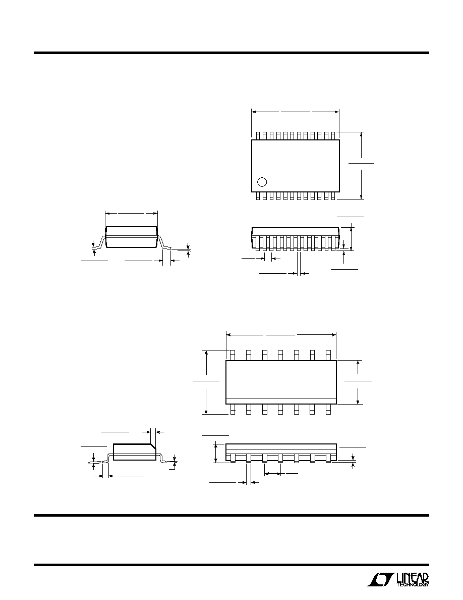
G Package
24-Lead Plastic SSOP
RELATED PARTS
See PCMCIA Product Family table on the first page of this data sheet.
1
2
3
4
0.150 ≠ 0.157*
(3.810 ≠ 3.988)
14
13
0.337 ≠ 0.344*
(8.560 ≠ 8.738)
0.228 ≠ 0.244
(5.791 ≠ 6.197)
12
11
10
9
5
6
7
8
0.016 ≠ 0.050
0.406 ≠ 1.270
0.010 ≠ 0.020
(0.254 ≠ 0.508)
◊
45
∞
0
∞
≠ 8
∞
TYP
0.008 ≠ 0.010
(0.203 ≠ 0.254)
SO14 0294
0.053 ≠ 0.069
(1.346 ≠ 1.752)
0.014 ≠ 0.019
(0.355 ≠ 0.483)
0.004 ≠ 0.010
(0.101 ≠ 0.254)
0.050
(1.270)
TYP
*THESE DIMENSIONS DO NOT INCLUDE MOLD FLASH OR PROTRUSIONS.
MOLD FLASH OR PROTRUSIONS SHALL NOT EXCEED 0.006 INCH (0.15mm).
S Package
14-Lead Plastic SOIC
24SSOP 0694
0.005 ≠ 0.009
(0.13 ≠ 0.22)
0
∞
≠ 8
∞
0.022 ≠ 0.037
(0.55 ≠ 0.95)
0.205 ≠ 0.212*
(5.20 ≠ 5.38)
0.301 ≠ 0.311
(7.65 ≠ 7.90)
1
2 3
4
5
6 7 8
9 10 11 12
0.318 ≠ 0.328*
(8.04 ≠ 8.33)
21
22
18 17 16 15 14 13
19
20
23
24
0.068 ≠ 0.078
(1.73 ≠ 1.99)
0.002 ≠ 0.008
(0.05 ≠ 0.21)
0.0256
(0.65)
BSC
0.010 ≠ 0.015
(0.25 ≠ 0.38)
*THESE DIMENSIONS DO NOT INCLUDE MOLD FLASH OR PROTRUSIONS.
MOLD FLASH OR PROTRUSIONS SHALL NOT EXCEED 0.006 INCH (0.15mm).