 | ÐлекÑÑоннÑй компоненÑ: LTC1337 | СкаÑаÑÑ:  PDF PDF  ZIP ZIP |
Äîêóìåíòàöèÿ è îïèñàíèÿ www.docs.chipfind.ru
1
LTC1337
5V Low Power RS232
3-Driver/5-Receiver Transceiver
S
FEATURE
D
U
ESCRIPTIO
s
Low Supply Current: 300
µ
A
s
1
µ
A Supply Current in SHUTDOWN
s
ESD Protection: Over
±
10kV
s
Operates from a Single 5V Supply
s
Uses Small Capacitors: 0.1
µ
F
s
Operates to 120k Baud
s
Three-State Outputs Are High Impedance When Off
s
Output Overvoltage Does Not Force Current Back into
Supplies
s
RS232 I/O Lines Can Be Forced to
±
25V without
Damage
s
Pin Compatible with LT1137A and LT1237
s
Flowthrough Architecture
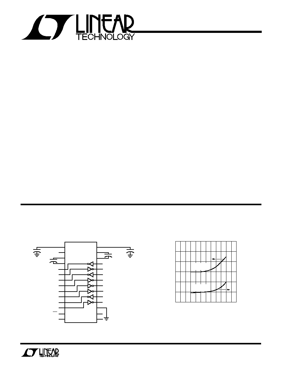
The LTC1337 is a 3-driver/ 5-receiver RS232 transceiver
with very low supply current. In the no load condition, the
supply current is only 300
µ
A. The charge pump only
requires four 0.1
µ
F capacitors and can supply up to 12mA
of extra current to power external circuitry.
In SHUTDOWN mode, the supply current is further re-
duced to 1
µ
A. All RS232 outputs assume a high imped-
ance state in SHUTDOWN and with the power off.
The LTC1337 is fully compliant with all data rate and
overvoltage RS232 specifications. The transceiver can
operate up to 120k baud with a 1000pF// 3k
load. Both
driver outputs and receiver inputs can be forced to
±
25V
without damage, and can survive multiple
±
10kV ESD
strikes.
U
S
A
O
PPLICATI
s
Notebook Computers
s
Palmtop Computers
U
A
O
PPLICATI
TYPICAL
3-Drivers/5-Receivers with SHUTDOWN
Supply Current
1337 TA01
V
CC
C1
0.1
µ
F
LTC1337
1
2
3
4
5
6
7
8
9
10
11
12
13
14
DRIVER 1 OUT
RX1 IN
DRIVER 2 OUT
RX2 IN
RX3 IN
RX4 IN
DRIVER 3 OUT
RX5 IN
ON/OFF
28
27
26
25
24
23
22
21
20
19
18
17
16
15
C3
0.1
µ
F
DRIVER 1 IN
RX1 OUT
DRIVER 2 IN
RX2 OUT
RX3 OUT
RX4 OUT
DRIVER 3 IN
RX5 OUT
V
V
+
C2
0.1
µ
F
C4
0.1
µ
F
GND
TEMPERATURE (°C)
QUIESCENT CURRENT OPERATING (
µ
A)
600
500
400
300
200
100
0
20
40
60
1337 TA02
80
0
20
1.2
1.0
0.8
0.6
0.4
0.2
0
SHUTDOWN CURRENT (
µ
A)
QUIESCENT
CURRENT
SHUTDOWN
CURRENT
TEST CONDITION:
V
CC
= 5V, ALL DRIVER INPUTS TIED TO V
CC
2
LTC1337
LTC1337CG
LTC1337CN
LTC1337CS
A
U
G
W
A
W
U
W
A
R
BSOLUTE
XI
TI
S
W
U
U
PACKAGE/ORDER I FOR ATIO
ORDER PART
NUMBER
Supply Voltage (V
CC
) ................................................ 6V
Input Voltage
Driver ....................................... 0.3V to V
CC
+ 0.3V
Receiver ............................................... 25V to 25V
On/Off Pin .................................. 0.3V to V
CC
+ 0.3V
Output Voltage
Driver .................................................... 25V to 25V
Receiver .................................... 0.3V to V
CC
+ 0.3V
Short Circuit Duration
V
+
................................................................... 30 sec
V
................................................................... 30 sec
Driver Output .............................................. Indefinite
Receiver Output .......................................... Indefinite
Operating Temperature Range
Commercial (LTC1337C) ........................ 0
°
C to 70
°
C
Storage Temperature Range ................ 65
°
C to 150
°
C
Lead Temperature (Soldering, 10 sec)................. 300
°
C
(Note 1)
1
2
3
4
5
6
7
8
9
10
11
12
13
14
V
+
V
CC
C1
+
C1
DR1 OUT
RX1 IN
DR2 OUT
RX2 IN
RX3 IN
RX4 IN
DR3 OUT
RX5 IN
ON/OFF
NC
28
27
26
25
24
23
22
21
20
19
18
17
16
15
V
C2
+
C2
DR1 IN
RX1 OUT
DR2 IN
RX2 OUT
RX3 OUT
RX4 OUT
DR3 IN
RX5 OUT
GND
NC
NC
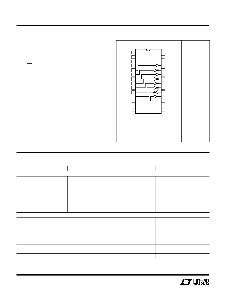
N PACKAGE
28-LEAD PLASTIC DIP
TOP VIEW
S PACKAGE
28-LEAD PLASTIC SOL
G PACKAGE
28-LEAD SSOP
T
JMAX
= 125
°
C,
JA
= 96
°
C/W (G)
T
JMAX
= 125
°
C,
JA
= 56
°
C/W (N)
T
JMAX
= 125
°
C,
JA
= 85
°
C/W (S)
Consult factory for Industrial and Military grade parts.
PARAMETER
CONDITIONS
MIN
TYP
MAX
UNITS
Any Driver
Output Voltage Swing
R
L
= 3k to GND
Positive
q
5.0
7.0
V
R
L
= 3k to GND
Negative
q
5.0
6.5
V
Logic Input Voltage Level
Input Low Level (V
OUT
= High)
q
1.4
0.8
V
Input High Level (V
OUT
= Low)
q
2.0
1.4
V
Logic Input Current
V
IN
= 5V
q
5
µ
A
V
IN
= 0
q
5
µ
A
Output Short-Circuit Current
V
OUT
= 0V
±
10
mA
Output Leakage Current
SHUTDOWN, V
OUT
=
±
20V (Note 3)
q
10
200
µ
A
Any Receiver
Input Voltage Thresholds
Input Low Threshold
q
0.8
1.3
V
Input High Threshold
q
1.7
2.4
V
Hysteresis
q
0.1
0.4
1
V
Input Resistance
3
5
7
k
Output Voltage
Output Low, I
OUT
= 1.6mA (V
CC
= 5V)
q
0.2
0.4
V
Output High, I
OUT
= 160
µ
A (V
CC
= 5V)
q
3.5
4.8
V
Output Short-Circuit Current
Sourcing Current, V
OUT
= 0
15
20
mA
Sinking Current, V
OUT
= V
CC
15
40
mA
Output Leakage Current
SHUTDOWN, 0
V
OUT
V
CC
(Note 3)
q
1
10
µ
A
ELECTRICAL C
C
HARA TERISTICS
C
D
V
CC
= 5V, C1 = C2 = C3 = C4 = 0.1
µ
F, unless otherwise noted.
3
LTC1337
ELECTRICAL C
C
HARA TERISTICS
C
D
V
CC
= 5V, C1 = C2 = C3 = C4 = 0.1
µ
F, unless otherwise noted.
C
C
HARA TERISTICS
U
W
A
TYPICAL PERFOR
CE
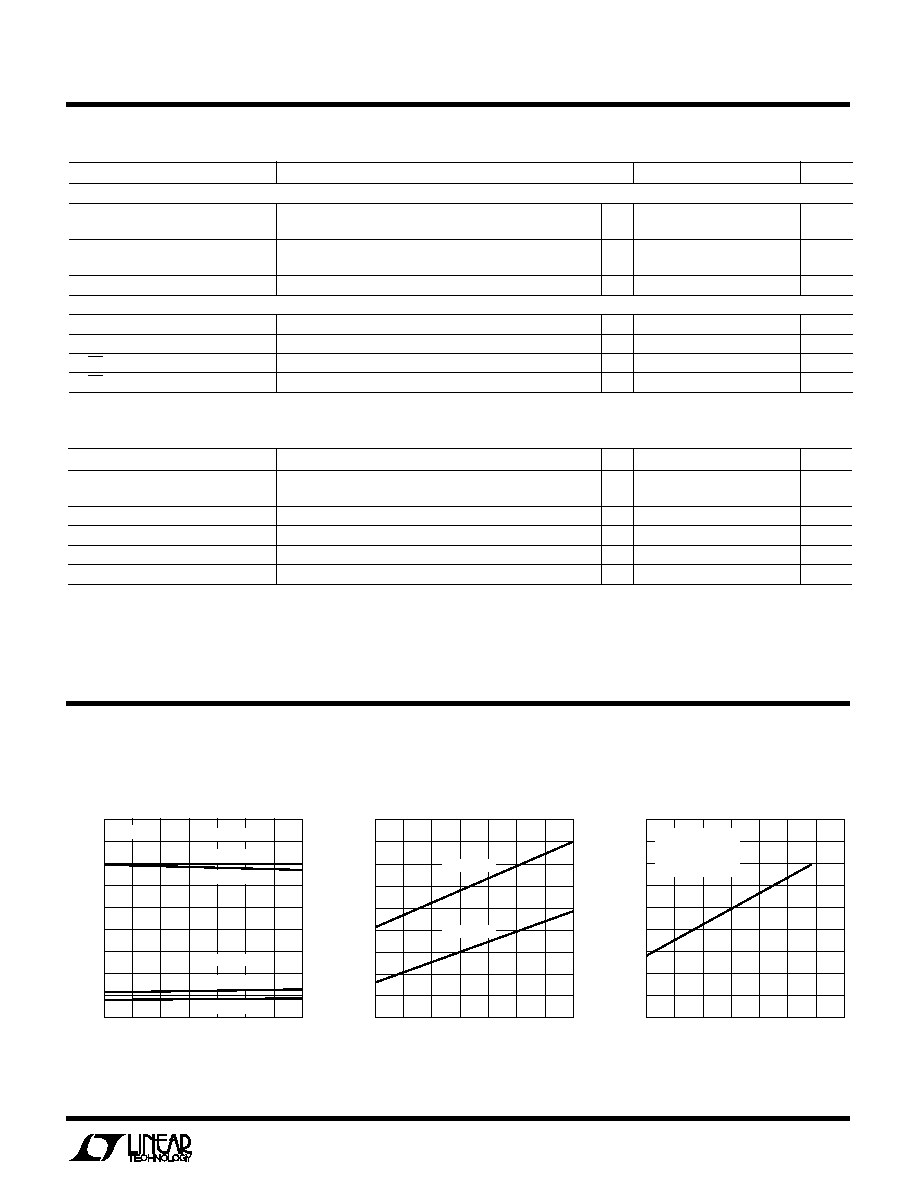
TEMPERATURE (°C)
0
THRESHOLD VOLTAGE (V)
60
2.0
1.9
1.8
1.7
1.6
1.5
1.4
1.3
1.2
1.1
1337 G02
20
70
10
30
40
50
INPUT HIGH
INPUT LOW
Driver Output Voltage
Receiver Input Thresholds
Supply Current vs Data Rate
DATA RATE (k BAUD)
0
SUPPLY CURRENT (mA)
150
45
40
35
30
25
20
15
10
5
0
1337 G03
50
175
25
75
100
125
V
CC
= 5V
R
L
= 3k
C
L
= 2500pF
3 DRIVERS ACTIVE
TEMPERATURE (°C)
0
DRIVER OUTPUT VOLTAGE (V)
60
10
8
6
4
2
0
2
4
6
8
1337 G01
20
70
10
30
40
50
V
CC
= 5V
OUTPUT HIGH
V
CC
= 4.5V
R
L
= 3k
V
CC
= 5V
V
CC
= 4.5V
OUTPUT LOW
The
q
denotes specifications which apply over the operating temperature
range (0
°
C
T
A
70
°
C).
Note 1: Absolute maximum ratings are those values beyond which the life
of the device may be impaired.
Note 2: Supply current is measured with driver and receiver outputs
unloaded and driver inputs tied high.
Note 3: Supply current and leakage measurements in SHUTDOWN are
performed with V
ON
= 0V.
PARAMETER
CONDITIONS
MIN
TYP
MAX
UNITS
Slew Rate
R
L
= 3k, C
L
= 51pF
8
30
V/
µ
s
R
L
= 3k, C
L
= 2500pF
2
4
V/
µ
s
Driver Propagation Delay
t
HLD
(Figure 1)
q
2
3
µ
s
(TTL to RS232)
t
LHD
(Figure 1)
q
2
3
µ
s
Receiver Propagation Delay
t
HLR
(Figure 2)
q
0.3
0.6
µ
s
(RS232 to TTL)
t
LHR
(Figure 2)
q
0.2
0.6
µ
s
PARAMETER
CONDITIONS
MIN
TYP
MAX
UNITS
Power Supply Generator
V
+
Output Voltage
I
OUT
= 0mA
8.0
V
I
OUT
= 12mA
7.5
V
V
Output Voltage
I
OUT
= 0mA
8.0
V
I
OUT
= 12mA
6.5
V
Supply Rise Time
SHUTDOWN to Turn-On
0.2
ms
Power Supply
V
CC
Supply Current
No Load (Note 2)
q
0.3
0.5
mA
Supply Leakage Current (V
CC
)
SHUTDOWN (Note 3)
q
1
10
µ
A
On/Off Threshold Low
q
1.4
0.8
V
On/Off Threshold High
q
2.0
1.4
V
C
C
HARA TERISTICS
AC
4
LTC1337
C
C
HARA TERISTICS
U
W
A
TYPICAL PERFOR
CE
V
CC
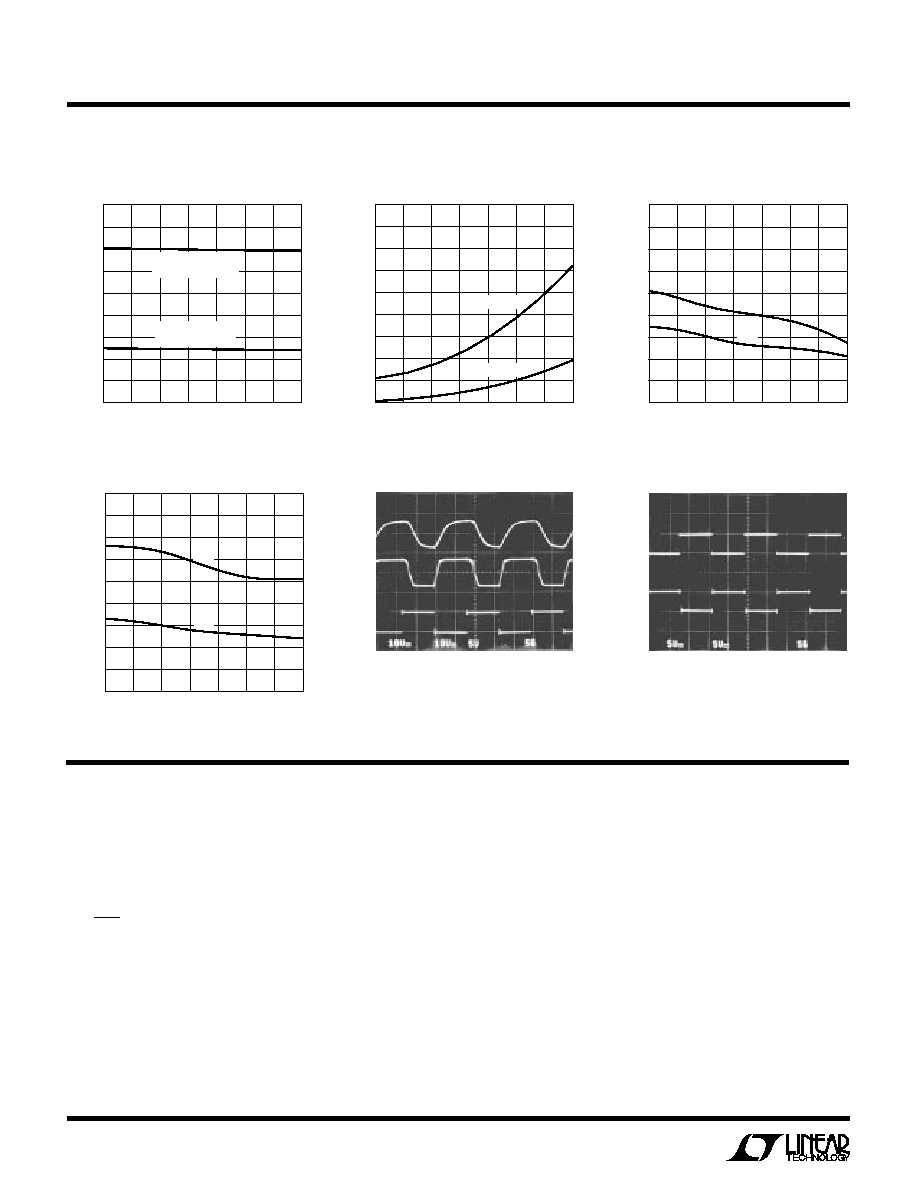
Supply Current
TEMPERATURE (°C)
0
LEAKAGE CURRENT (
µ
A)
60
45
40
35
30
25
20
15
10
5
0
1337 G05
20
70
10
30
40
50
V
OUT
= 20V
V
OUT
= 20V
TEMPERATURE (°C)
0
SUPPLY CURRENT (mA)
60
20
16
14
12
10
8
6
4
2
0
1337 G04
20
70
10
30
40
50
3 DRIVERS LOADED
R
L
= 3k
1 DRIVER LOADED
R
L
= 3k
Driver Short-Circuit Current
Driver Leakage in SHUTDOWN
Receiver Short-Circuit Current
Driver Output Waveforms
INPUT
DRIVER
OUTPUT
R
L
= 3k
DRIVER
OUTPUT
R
L
= 3k
C
L
= 2500pF
Receiver Output Waveforms
RX
OUTPUT
C
L
= 50pF
INPUT
PI FU CTIO S
U
U
U
V
CC
: 5V Input Supply Pin. Supply current less than 1
µ
A in
the SHUTDOWN mode. This pin should be decoupled with
a 0.1
µ
F ceramic capacitor.
GND: Ground Pin.
ON/OFF: TTL/CMOS Compatible Shutdown Pin. A logic
low puts the device in the SHUTDOWN mode which
reduces input supply current to less than 1
µ
A and places
all drivers and receivers in high impedance state.
V
+
: Positive Supply Output (RS232 Drivers). V
+
2V
CC
1V. This pin requires an external capacitor C = 0.1
µ
F for
charge storage. The capacitor may be tied to ground or 5V.
With multiple devices, the V
+
and V
pins may be paral-
leled into common capacitors. For large numbers of
devices, increasing the size of the shared common storage
capacitors is recommended to reduce ripple.
V
: Negative Supply Output (RS232 Drivers). V
(2V
CC
1.5V). This pin requires an external capacitor C = 0.1
µ
F
for charge storage.
C1
+
, C1
, C2
+
, C2
: Commutating Capacitor Inputs. These
pins require two external capacitors C = 0.1
µ
F. One from
C1
+
to C1
, and another from C2
+
to C2
. To maintain
charge pump efficiency, the capacitor's effective series
resistance should be less than 50
.
TEMPERATURE (°C)
0
SHORT-CIRCUIT CURRENT (mA)
60
20
18
16
14
12
10
8
6
4
2
1337 G06
20
70
10
30
40
50
I
SC
+
I
SC
TEMPERATURE (°C)
0
SHORT-CIRCUIT CURRENT (mA)
60
55
50
45
40
35
30
25
20
15
10
1337 G07
20
70
10
30
40
50
I
SC
+
I
SC
5
LTC1337
PI FU CTIO S
U
U
U
DRIVER IN: RS232 Driver Input Pins. Inputs are TTL/
CMOS compatible. Inputs should not be allowed to float.
Tie unused inputs to V
CC
.
DRIVER OUT: Driver Outputs at RS232 Voltage Levels.
Outputs are in a high impedance state when in SHUT-
DOWN mode or V
CC
= 0V. The driver outputs are protected
against ESD to
±
10kV for human body model discharges.
RX IN: Receiver Inputs. These pins can be forced to
±
25V
without damage. The receiver inputs are protected against
ESD to
±
10kV for human body model discharges. Each
receiver provides 0.4V of hysteresis for noise immunity.
RX OUT: Receiver Outputs with TTL/CMOS Voltage Lev-
els. Outputs are in a high impedance state when in SHUT-
DOWN mode to allow data line sharing.
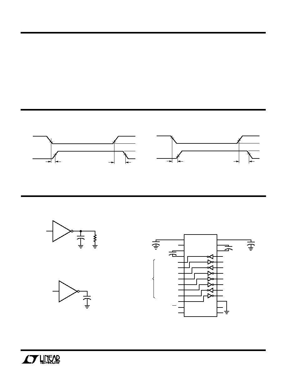
Figure 1. Driver Propagation Delay Timing
0.8V
V
CC
0V
0V
RX IN
RX
OUTPUT
1.3V
t
HLR
1.7V
t
LHR
1337 F02
V
CC
0V
Figure 2. Receiver Propagation Delay Timing
TI
W
E WAVEFOR
S
U
G
WITCHI
W
S
TEST CIRCUITS
DRIVER
DRIVER
INPUT
3k
51pF
DRIVER
OUTPUT
1337 F03
Figure 3. Driver Timing Test Load
ESD Test Circuit
1.4V
0V
V
CC
0V
V
+
V
0V
DRIVER
INPUT
DRIVER
OUTPUT
1.4V
t
HLD
t
LHD
1337 F01
1337 TC01
V
CC
C1
0.1
µ
F
LTC1337
1
2
3
4
5
6
7
8
9
10
11
12
13
14
DRIVER 1 OUT
RX1 IN
DRIVER 2 OUT
RX2 IN
RX3 IN
RX4 IN
DRIVER 3 OUT
RX5 IN
ON/OFF
28
27
26
25
24
23
22
21
20
19
18
17
16
15
C3
0.1
µ
F
DRIVER 1 IN
RX1 OUT
DRIVER 2 IN
RX2 OUT
RX3 OUT
RX4 OUT
DRIVER 3 IN
RX5 OUT
V
V
+
C2
0.1
µ
F
C4
0.1
µ
F
GND
RS232
LINE PINS
PROTECTED
TO ±10kV
RX
RX IN
51pF
RX
OUTPUT
1337 F04
Figure 4. Receiver Timing Test Load