 | ÐлекÑÑоннÑй компоненÑ: LTC1380 | СкаÑаÑÑ:  PDF PDF  ZIP ZIP |
Äîêóìåíòàöèÿ è îïèñàíèÿ www.docs.chipfind.ru
1
LTC1380/LTC1393
Single-Ended 8-Channel/
Differential 4-Channel Analog
Multiplexer with SMBus Interface
V
S
(V)
5
ON RESISTANCE (
)
150
200
250
3
1167 G15
100
50
125
175
225
75
25
0
3
1
1
4
4
2
0
2
5
V
CC
= 2.7V
V
EE
= 0V
T
A
= 25
°
C
I
D
= 1mA
V
CC
= 5V
V
EE
= 0V
V
CC
= 5V
V
EE
= 5V
On Resistance vs V
S
1
2
3
4
5
6
7
8
16
15
14
13
12
11
10
9
LTC1380
0.1
µ
F
15k
8 ANALOG
INPUTS
15k
0.1
µ
F
5V
5V
ANALOG OUTPUT
1380/93 TA01
S0
S1
S2
S3
S4
S5
S6
S7
V
CC
SCL
SDA
A0
A1
GND
V
EE
D
O
SMBus
HOST
SCL
SDA
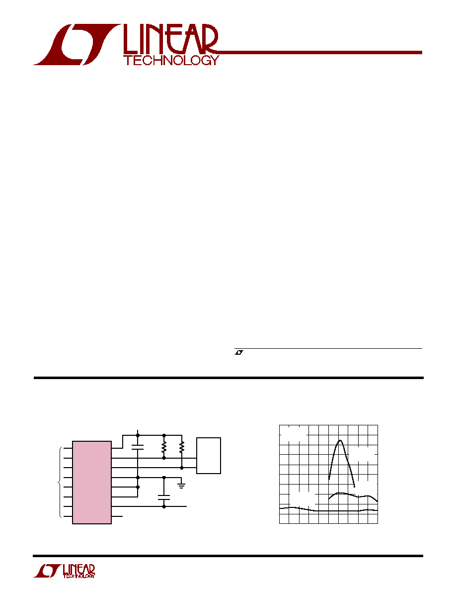
LTC1380 Single-Ended 8-Channel Multiplexer
TYPICAL APPLICATIO
N
U
The LTC
®
1380/LTC1393 are CMOS analog multiplexers with
SMBus
®
compatible digital interfaces. The LTC1380 is a
single-ended 8-channel multiplexer, while the LTC1393 is a
differential 4-channel multiplexer. The SMBus digital inter-
face requires only two wires (SCL and SDA). Both the
LTC1380 and the LTC1393 have four hard-wired SMBus
addresses, selectable with two external address pins. This
allows four devices, each with a unique SMBus address, to
coexist on one system and for four devices to be synchro-
nized with one stop bit.
The supply current is typically 10
µ
A. Both digital interface
pins are SMBus compatible over the full operating supply
voltage range. The LTC1380 analog switches feature a
typical R
ON
of 35
(
±
5V supplies), typical switch leakage of
20pA and guaranteed break-before-make operation. Charge
injection is
±
1pC typical.
The LTC1380/LTC1393 are available in 16-lead SO and GN
packages. Operation is fully specified over the commercial
and industrial temperature ranges.
s
Micropower Operation: Supply Current = 20
µ
A Max
s
2-Wire SMBus Interface
s
Single 2.7V to
±
5V Supply Operation
s
Expandable to 32 Single or 16 Differential Channels
s
Guaranteed Break-Before-Make
s
Low R
ON
: 35
Single Ended/70
Differential
s
Low Charge Injection: 20pC Max
s
Low Leakage:
±
5nA Max
s
Available in 16-Lead SO and GN Packages
FEATURES
DESCRIPTIO
N
U
, LTC and LT are registered trademarks of Linear Technology Corporation.
SMBus is a registered trademark of Intel Corporation.
s
Data Acquisition Systems
s
Process Control
s
Laptop Computers
s
Signal Multiplexing/Demultiplexing
s
Analog-to-Digital Conversion Systems
APPLICATIO
N
S
U
2
LTC1380/LTC1393
ABSOLUTE
M
AXI
M
U
M
RATINGS
W
W
W
U
(Note 1)
Total Supply Voltage
LTC1380 (V
CC
to V
EE
) ......................................... 15V
LTC1393 (V
CC
to GND) ....................................... 15V
Analog Input Voltage
LTC1380 ............................. V
EE
0.3V to V
CC
+ 0.3V
LTC1393 ................................... 0.3V to V
CC
+ 0.3V
Digital Inputs ............................................. 0.3V to 15V
LTC1380 (V
CC
TO V
EE
) .... (V
EE
0.3V) to (V
EE
+ 15V)
LTC1393 (V
CC
to GND) .......................... 0.3V to 15V
Maximum Switch-On Current .............................. 65mA
Power Dissipation ............................................. 500mW
Operating Ambient Temperature Range
LTC1380C/LTC1393C ....................... 0
°
C
T
A
70
°
C
LTC1380I/LTC1393I .................... 40
°
C
T
A
85
°
C
Junction Temperature ........................................... 125
°
C
Storage Temperature Range ................. 65
°
C to 150
°
C
Lead Temperature (Soldering, 10 sec) .................. 300
°
C
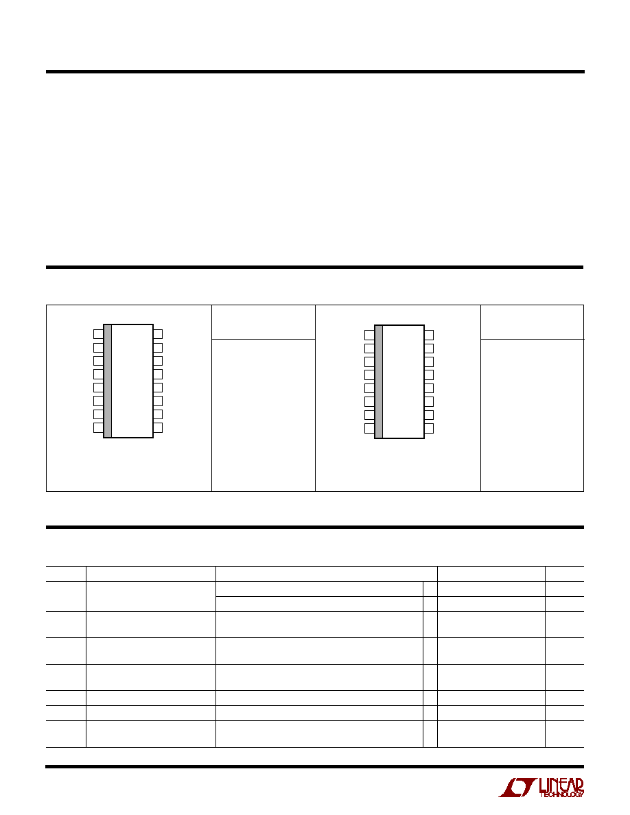
PACKAGE/ORDER I
N
FOR
M
ATIO
N
W
U
U
ORDER PART
NUMBER
ORDER PART
NUMBER
LTC1393CGN
LTC1393CS
LTC1393IGN
LTC1393IS
LTC1380CGN
LTC1380CS
LTC1380IGN
LTC1380IS
TOP VIEW
S PACKAGE
16-LEAD PLASTIC SO
GN PACKAGE
16-LEAD PLASTIC SSOP
1
2
3
4
5
6
7
8
16
15
14
13
12
11
10
9
S0
S1
S2
S3
S4
S5
S6
S7
V
CC
SCL
SDA
A0
A1
GND
V
EE
D
O
T
JMAX
= 125
°
C,
JA
= 130
°
C/ W (GN)
T
JMAX
= 125
°
C,
JA
= 100
°
C/ W (S)
T
JMAX
= 125
°
C,
JA
= 130
°
C/ W (GN)
T
JMAX
= 125
°
C,
JA
= 100
°
C/ W (S)
TOP VIEW
S PACKAGE
16-LEAD PLASTIC SO
GN PACKAGE
16-LEAD PLASTIC SSOP
1
2
3
4
5
6
7
8
16
15
14
13
12
11
10
9
S0
+
S0
S1
+
S1
S2
+
S2
S3
+
S3
V
CC
SCL
SDA
A0
A1
GND
D
O
D
O
+
Consult factory for Military grade parts.
ELECTRICAL CHARACTERISTICS
SYMBOL
PARAMETER
CONDITIONS
MIN
TYP
MAX
UNITS
V
ANALOG
Analog Signal Range
LTC1380
q
V
EE
V
CC
V
LTC1393
q
0
V
CC
V
R
ON
On Resistance
LT1380: V
CC
= 5V, V
EE
= 5V,
35
70
V
EE
(V
S
, V
D
)
V
CC
, I
D
=
±
1mA
q
120
LT1393: V
CC
= 5V,
70
140
0V
(V
S
, V
D
)
V
CC
, I
D
=
±
1mA
q
200
LT1380/LTC1393: V
CC
= 2.7V, V
EE
= 0V,
210
400
0V
(V
S
, V
D
)
V
CC
, I
D
=
±
1mA
q
600
R
ON
vs V
S
V
EE
(V
S
, V
D
)
V
CC
, V
CC
= 5V
20
%
R
ON
vs Temperature
V
CC
= 5V
0.5
%/
°
C
I
LEAK
Off-Channel or On-Channel
LTC1380: (V
EE
+ 0.5V)
(V
S
, V
D
)
(V
CC
0.5V)
±
0.05
±
5
nA
Switch Leakage
LTC1393: 0.5V
(V
S
, V
D
)
(V
CC
0.5V)
q
±
50
nA
(Notes 2, 4)
3
LTC1380/LTC1393
ELECTRICAL CHARACTERISTICS
(Notes 2, 4)
The
q
denotes specifications which apply over the full operating
temperature range.
Note 1: Absolute Maximum Ratings are those values beyond which the life
of a device may be impaired.
Note 2: All current into device pins is positive; all current out of device
pins is negative. All voltages are referenced to ground unless otherwise
specified. All typicals are given for T
A
= 25
°
C, V
CC
= 5V (for both LTC1380
and LTC1393) and V
EE
= 5V (LTC1380).
Note 3: These typical parameters are based on bench measurements and
are not production tested.
Note 4: Both SCL and SDA assume an external 15k pull-up resistor to a
typical SMBus host power supply V
DD
of 5V.
Note 5: Typical curves with V
EE
= 5V apply to the LTC1380. Curves with
V
EE
= 0V apply to both the LTC1380 and the LTC1393.
Note 6: These parameters are guaranteed by design and are not tested in
production.
SYMBOL
PARAMETER
CONDITIONS
MIN
TYP
MAX
UNITS
V
IH
SCL, SDA Input High Voltage
q
1.4
V
V
IL
SCL, SDA Input Low Voltage
q
0.6
V
V
OL
SDA Output Low Voltage
I
SDA
= 3mA
q
0.4
V
V
AH
Address Input High Voltage
V
CC
= 5V
q
2
V
V
AL
Address Input Low Voltage
V
CC
= 5V
q
0.8
V
I
IN
SCL, SDA, Address Input Current
0V
V
IN
V
CC
±
1
µ
A
I
CC
Positive Supply Current
V
CC
= 5V, All Digital Inputs at 5V
q
10
20
µ
A
I
EE
Negative Supply Current
LTC1380: V
CC
= 5V, V
EE
= 5V, All Digital Inputs at 5V
q
0.1
5
µ
A
C
S
Input Off Capacitance
(Note 3)
3
pF
C
D
Output Off Capacitance
(Note 3) LTC1380
26
pF
LTC1393
18
pF
t
ON
Switch Turn-On Time from
Figure 1 LTC1380: V
CC
= 5V, V
EE
= 5V
q
850
1500
ns
Stop Condition
LTC1393: V
CC
= 5V
q
850
1500
ns
LTC1380/LTC1393: V
CC
= 2.7V, V
EE
= 0V
q
1130
2000
ns
t
OFF
Switch Turn-Off Time from
Figure 1 LTC1380: V
CC
= 5V, V
EE
= 5V
q
640
1200
ns
Stop Condition
LTC1393: V
CC
= 5V
q
650
1200
ns
LTC1380/LTC1393: V
CC
= 2.7V, V
EE
= 0V
q
670
1200
ns
t
OPEN
Break-Before-Make Interval
t
ON
t
OFF
q
75
210
ns
OIRR
Off-Channel Isolation
Figure 2, V
S
= 200mV
P-P
, R
L
= 1k, f = 100kHz (Note 3)
65
dB
Q
INJ
Charge Injection
Figure 3, C
L
= 1000pF (Note 3)
q
±
1
±
20
pC
SMBus Timing (Note 6)
f
SMB
SMBus Operating Frequency
q
100
kHz
t
BUF
Bus Free Time Between Stop/Start
q
4.7
µ
s
t
HD:STA
Hold Time After (Repeated) Start
q
4.0
µ
s
t
SU:STA
Repeated Start Setup Time
q
4.7
µ
s
t
SU:STO
Stop Condition Setup Time
q
4.0
µ
s
t
HD:DAT
Data Hold Time
q
300
ns
t
SU:DAT
Data Setup Time
q
250
ns
t
LOW
Clock Low Period
q
4.7
µ
s
t
HIGH
Clock High Period
q
4.0
µ
s
t
f
SCL/SDA Fall Time
Time Interval Between 0.9V
DD
and (V
ILMAX
0.15)
q
300
ns
t
r
SCL/SDA Rise Time
Time Interval Between (V
ILMAX
0.15)
q
1000
ns
and (V
IHMIN
+ 0.15)
4
LTC1380/LTC1393
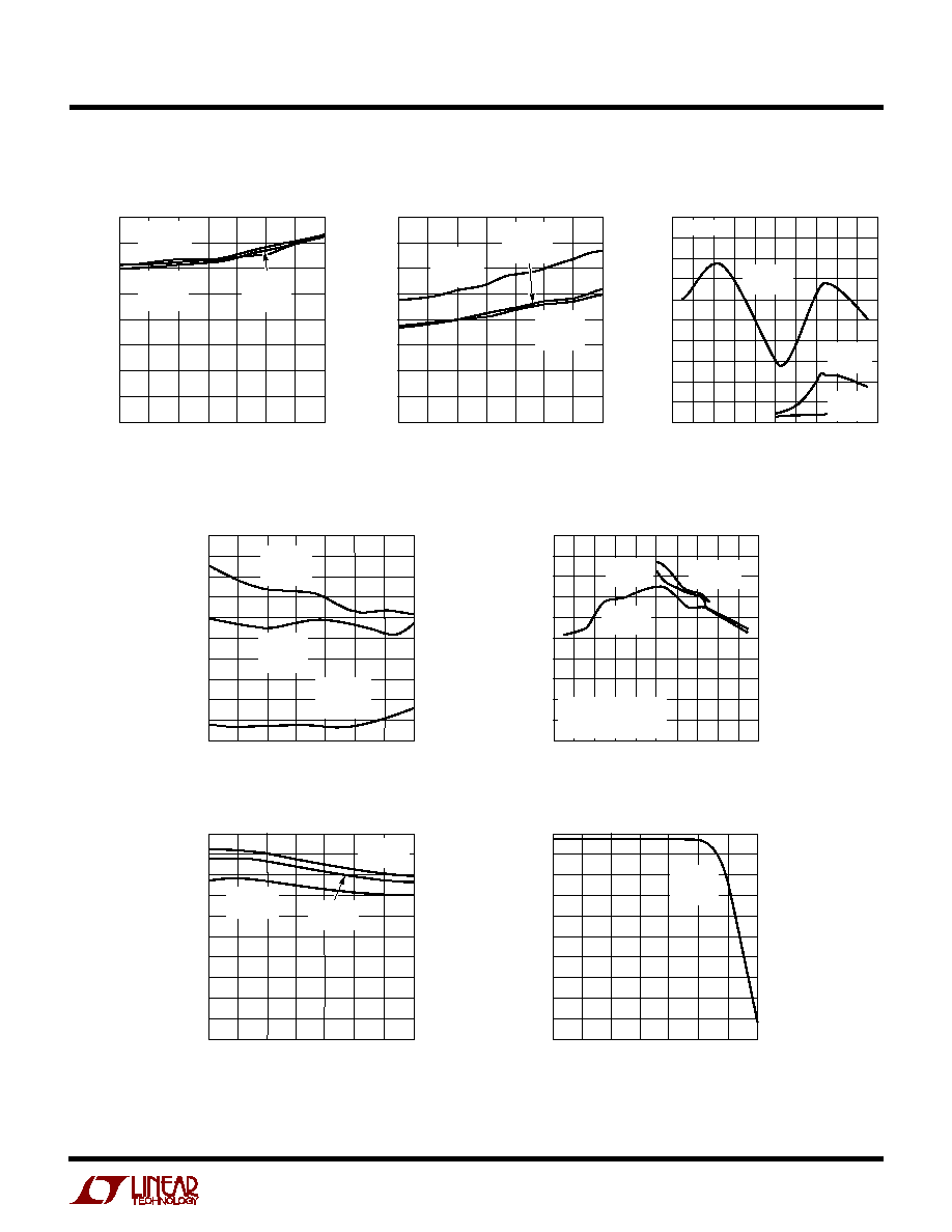
TYPICAL PERFOR A CE CHARACTERISTICS
U
W
V
S
(V)
4.5
I
S
LEAKAGE (nA)
0.010
2.5
0.5 0.5
4.5
1380/93 G04
0.008
0.006
0.004
0.002
0
0.002
0.004
0.006
0.008
0.010
3.5
1.5
1.5 2.5 3.5
T
A
= 25
°
C
V
CC
= 5V
V
EE
= 5V
V
CC
= 5V
V
EE
= 0V
V
CC
= 2.7V
V
EE
= 0V
Off-Channel Output Leakage
vs Temperature
TEMPERATURE (
°
C)
50
1
10
1000
25
75
1380/93 G07
0.1
0.01
25
0
50
100
125
0.001
0.0001
100
I
D
LEAKAGE (nA)
V
CC
= 2.7V
V
EE
= 0V
V
D
= 1.35V
V
CC
= 5V
V
EE
= 5V
V
D
= 0V
V
CC
= 5V
V
EE
= 0V
V
D
= 2.5V
Off-Channel Input Leakage
vs Temperature
TEMPERATURE (
°
C)
50
25
0.0001
I
S
LEAKAGE (nA)
0.01
10
0
50
75
1380/93 G06
0.001
1
0.1
25
100
125
V
CC
= 5V
V
EE
= 0V
V
S
= 2.5V
V
CC
= 5V
V
EE
= 5V
V
S
= 0V
V
CC
= 2.7V
V
EE
= 0V
V
S
= 1.35V
On-Channel Output Leakage vs V
D
V
D
(V)
4.5
I
D
LEAKAGE (nA)
0.010
2.5
0.5 0.5
4.5
1380/93 G05
0.008
0.006
0.004
0.002
0
0.002
0.004
0.006
0.008
0.010
3.5
1.5
1.5 2.5 3.5
T
A
= 25
°
C
V
CC
= 5V
V
EE
= 5V
V
CC
= 5V
V
EE
= 0V
V
CC
= 2.7V
V
EE
= 0V
TEMPERATURE (
°
C)
50
0
ON RESISTANCE (
)
25
75
100
125
250
175
0
50
75
1380/93 G01
50
200
225
150
25
25
100
125
I
D
= 1mA
V
CC
= 2.7V
V
EE
= 0V
V
S
= 1.35V
V
CC
= 5V
V
EE
= 0V
V
S
= 2.5V
V
CC
= 5V
V
EE
= 5V
V
S
= 0V
On Resistance vs Temperature
V
S
(V)
4.5
I
S
LEAKAGE (nA)
0.0020
2.5
0.5 0.5
4.5
1380/93 G02
0.0018
0.0016
0.0014
0.0012
0.0010
0.0008
0.0006
0.0004
0.0002
0
3.5
1.5
1.5 2.5 3.5
T
A
= 25
°
C
V
CC
= 5V
V
EE
= 5V
V
CC
= 5V
V
EE
= 0V
V
CC
= 2.7V
V
EE
= 0V
V
D
(V)
4.5
I
D
LEAKAGE (nA)
0.010
2.5
0.5 0.5
4.5
1380/93 G03
0.008
0.006
0.004
0.002
0
0.002
0.004
0.006
0.008
0.010
3.5
1.5
1.5 2.5 3.5
T
A
= 25
°
C
V
CC
= 5V
V
EE
= 5V
V
CC
= 2.7V
V
EE
= 0V
V
CC
= 5V
V
EE
= 0V
Off-Channel Output Leakage vs V
D
On-Channel Input Leakage
vs Temperature
TEMPERATURE (
°
C)
50
1
10
1000
25
75
1380/93 G08
0.1
0.01
25
0
50
100
125
0.001
0.0001
100
I
S
LEAKAGE (nA)
V
CC
= 5V
V
EE
= 5V
V
S
= 0V
V
CC
= 5V
V
EE
= 0V
V
S
= 2.5V
V
CC
= 2.7V
V
EE
= 0V
V
S
= 1.35V
TEMPERATURE (
°
C)
50
1
10
1000
25
75
1380/93 G09
0.1
0.01
25
0
50
100
125
0.001
0.0001
100
I
D
LEAKAGE (nA)
V
CC
= 5V
V
EE
= 5V
V
D
= 0V
V
CC
= 5V
V
EE
= 0V
V
D
= 2.5V
V
CC
= 2.7V
V
EE
= 0V
V
D
= 1.35V
Off-Channel Input Leakage vs V
S
On-Channel Input Leakage vs V
S
On-Channel Output Leakage
vs Temperature
(Note 5)
5
LTC1380/LTC1393
TYPICAL PERFOR A CE CHARACTERISTICS
U
W
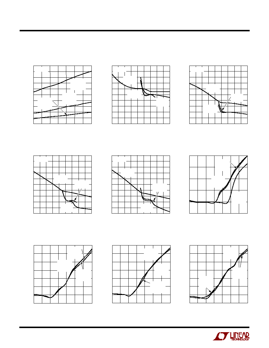
Off Time vs Temperature
Q
INJ
vs V
C
(Figure 3)
On Time vs Temperature
TEMPERATURE (
°
C)
50
ON TIME (ns)
1400
25
1380/93 G11
800
400
25
0
50
200
0
1600
1200
1000
600
75
100
125
V
CC
= 2.7V
V
EE
= 0V
V
S
= 1.35V
V
CC
= 5V
V
EE
= 0V
V
S
= 2.5V
V
CC
= 5V
V
EE
= 5V
V
S
= 0V
V
C
(V)
5
Q
INJ
(pC)
3.0
4.0
5.0
3
1380/93 G12
2.0
1.0
2.5
3.5
4.5
1.5
0.5
0
3
1
1
4
4
2
0
2
5
T
A
= 25
°
C
V
CC
= 5V
V
EE
= 5V
V
CC
= 2.7V
V
EE
= 0V
V
CC
= 5V
V
EE
= 0V
TEMPERATURE (
°
C)
50
OFF TIME (ns)
700
25
1380/93 G10
400
200
25
0
50
100
0
800
600
500
300
75
100
125
V
CC
= 5V
V
EE
= 5V
V
S
= 0V
V
CC
= 2.7V
V
EE
= 0V
V
S
= 1.35V
V
CC
= 5V
V
EE
= 0V
V
S
= 2.5V
Q
INJ
vs Temperature (Figure 3)
TEMPERATURE (
°
C)
50
0
Q
INJ
(pC)
0.2
0.6
0.8
1.0
2.0
1.4
0
50
75
1380/93 G13
0.4
1.6
1.8
1.2
25
25
100
125
V
CC
= 5V
V
EE
= 5V
V
S
= 0V
V
CC
= 2.7V
V
EE
= 0V
V
S
= 1.35V
V
CC
= 5V
V
EE
= 0V
V
S
= 2.5V
Off-Channel Isolation vs Input
Common Mode Voltage (Figure 2)
I
CC
vs Temperature
TEMPERATURE (
°
C)
50
0
I
CC
(
µ
A)
1
3
4
5
10
7
0
50
75
1380/93 G15
2
8
9
6
25
25
100
125
V
CC
= 5V
V
EE
= 5V
V
CC
= 2.7V
V
EE
= 0V
V
CC
= 5V
V
EE
= 0V
TEMPERATURE (
°
C)
50
100
I
EE
(nA)
90
70
60
50
0
30
0
50
75
1380/93 G16
80
20
10
40
25
25
100
125
V
CC
= 5V
V
EE
= 5V
V
S
= 0V
I
EE
vs Temperature
(Note 5)
V
C
(V)
5
OIRR (dB)
75
73
74
72
71
70
69
68
67
66
65
3
1380/93 G14
3
1
1
5
2
4
2
0
4
V
CC
= 5V
V
EE
= 5V
V
CC
= 5V
V
EE
= 0V
V
CC
= 2.7V
V
EE
= 0V
T
A
= 25
°
C
V
S
= 200mV
P-P
, 100kHz
R
L
= 1k