 | ÐлекÑÑоннÑй компоненÑ: LTC1390 | СкаÑаÑÑ:  PDF PDF  ZIP ZIP |
Äîêóìåíòàöèÿ è îïèñàíèÿ www.docs.chipfind.ru
1
LTC1390
8-Channel
Analog Multiplexer
with Serial Interface
S
FEATURE
D
U
ESCRIPTIO
The LTC
®
1390 is a high performance CMOS 8-to-1 analog
multiplexer. It features a 3-wire digital interface with a
bidirectional data retransmission feature, allowing it to be
wired in series with a serial A/D converter while using only
one serial port. The interface also allows several LTC1390s
to be wired in series or parallel, increasing the number of
MUX channels available using only a single digital port. All
the above features are also valid when LTC1390 operates
as a demultiplexer such as with a D/A converter.
The LTC1390 features a typical R
ON
of 45
, typical switch
leakage of 50pA, and guaranteed break-before-make op-
eration. Charge injection is
±
10pC maximum. All digital
inputs are TTL and CMOS compatible when operated from
single or dual supplies. The inputs can withstand 100mA
fault currents.
The LTC1390 is available in 16-pin PDIP and narrow SO
packages.
s
3-Wire Serial Digital Interface
s
Data Retransmission Allows Series Connection
with Serial A/D Converters
s
Single 3V to
±
5V Supply Operation
s
Analog Inputs May Extend to Supply Rails
s
Low Charge Injection
s
Low R
ON
: 75
Max
s
Low Leakage:
±
5nA Max
s
Guaranteed Break-Before-Make
s
TTL/CMOS Compatible for All Digital Inputs
s
Cascadable to Allow Additional Channels
s
Can Be Used as a Demultiplexer
s
Data Acquisition Systems
s
Communication Systems
s
Signal Multiplexing/Demultiplexing
U
S
A
O
PPLICATI
, LTC and LT are registered trademarks of Linear Technology Corporation.
U
A
O
PPLICATI
TYPICAL
ANALOG INPUT VOLTAGE, V
S
(V)
5
ON-RESISTANCE (
)
150
200
250
3
LTC1390 · TA02
100
50
0
3
1
1
4
4
2
0
2
5
V
+
= 3V
V
= 0V
V
+
= 5V
V
= 5V
T
A
= 25
°
C
ON-Resistance vs
Analog Input Voltage
1
2
3
4
5
6
7
8
16
15
14
13
12
11
10
9
S0
S1
S2
S3
S4
S5
S6
S7
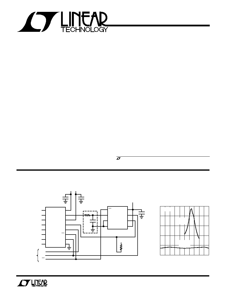
V
+
D
V
DATA 2
DATA 1
CS
CLK
GND
ANALOG
INPUTS
3-WIRE
SERIAL
INTERFACE
TO MUX AND ADC
DATA
CLK
CS
LTC1390
V
CC
V
CC
V
CC
47k
V
EE
1
2
3
4
8
7
6
5
CS
+IN
IN
GND
V
CC
CLK
D
OUT
V
REF
LTC1096
LTC1390 · TA01
OPTIONAL A/D
INPUT FILTER
2
LTC1390
A
U
G
W
A
W
U
W
A
R
BSOLUTE
XI
TI
S
W
U
U
PACKAGE/ORDER I FOR ATIO
(Note 1)
Total Supply Voltage (V
+
to V
) .............................. 15V
Input Voltage
Analog Inputs ........................ V
0.3V to V
+
+ 0.3V
Digital Inputs ........................................ 0.3V to 15V
Digital Outputs............................ 0.3V to V
+
+ 0.3V
Power Dissipation ............................................. 500mW
Operating Temperature Range ..................... 0
°
C to 70
°
C
Storage Temperature Range ................. 65
°
C to 150
°
C
Lead Temperature (Soldering, 10 sec) ................. 300
°
C
T
JMAX
= 150
°
C,
JA
= 70
°
C/ W (N)
T
JMAX
= 150
°
C,
JA
= 100
°
C/ W (S)
ORDER PART
NUMBER
LTC1390CN
LTC1390CS
Consult factory for Industrial and Military grade parts.
ELECTRICAL C
C
HARA TERISTICS
V
+
= 5V, V
= 5V, GND = 0V, T
A
= operating temperature unless otherwise noted.
SYMBOL
PARAMETER
CONDITIONS
MIN
TYP
MAX
UNITS
Switch
V
ANALOG
Analog Signal Range
(Note 2)
q
5
5
V
R
ON
On Resistance
V
S
=
±
3.5V, I
D
= 1mA
T
MIN
75
25
°
C
45
75
T
MAX
120
R
ON
vs V
S
20
%
R
ON
vs Temperature
0.5
%/
°
C
I
S(OFF)
Off Input Leakage
V
S
= 4V, V
D
= 4V; V
S
= 4V, V
D
= 4V
0.05
±
5
nA
Channel Off
q
±
50
nA
I
D(OFF)
Off Output Leakage
V
S
= 4V, V
D
= 4V; V
S
= 4V, V
D
= 4V
0.05
±
5
nA
Channel Off
q
±
50
nA
I
D(ON)
On Channel Leakage
V
S
= V
D
=
±
4V
0.05
±
5
nA
Channel On
q
±
50
nA
Input
V
INH
High Level Input Voltage
V
+
= 5.25V
q
2.4
V
V
INL
Low Level Input Voltage
V
+
= 4.75V
q
0.8
V
I
INL
, I
INH
Low or High Level Current
V
IN
= 5V, V
IN
= 0V
q
±
1
µ
A
V
OH
High Level Output Voltage
V
+
= 4.75V, I
O
= 10
µ
A
4.74
V
V
+
= 4.75V, I
O
= 360
µ
A
q
2.4
4.50
V
V
OL
Low Level Output Voltage
V
+
= 4.75V, I
O
= 0.5mA
q
0.16
0.8
V
1
2
3
4
5
6
7
8
TOP VIEW
S PACKAGE
16-LEAD PLASTIC SO
N PACKAGE
16-LEAD PDIP
16
15
14
13
12
11
10
9
S0
S1
S2
S3
S4
S5
S6
S7
V
+
D
V
DATA 2
DATA 1
CS
CLK
GND
3
LTC1390
ELECTRICAL C
C
HARA TERISTICS
V
+
= 5V, V
= 5V, GND = 0V, T
A
= operating temperature unless otherwise noted.
V
+
= 3V, V
= GND = 0V, T
A
= operating temperature unless otherwise noted.
SYMBOL
PARAMETER
CONDITIONS
MIN
TYP
MAX
UNITS
Switch
V
ANALOG
Analog Signal Range
(Note 2)
q
0
3
V
R
ON
On Resistance
V
S
= 1.2V, I
D
= 1mA
T
MIN
255
25
°
C
200
255
T
MAX
300
R
ON
vs V
S
20
%
R
ON
vs Temperature
0.5
%/
°
C
I
S(OFF)
Off Input Leakage
V
S
= 2.5V, V
D
= 0.5V; V
S
= 0.5V, V
D
= 2.5V (Note 3)
±
0.05
±
5
nA
Channel Off
q
±
50
nA
I
D(OFF)
Off Output Leakage
V
S
= 2.5V, V
D
= 0.5V; V
S
= 0.5V, V
D
= 2.5V (Note 3)
±
0.05
±
5
nA
Channel Off
q
±
50
nA
I
D(ON)
On Channel Leakage
V
S
= V
D
= 0.5V, V
S
= V
D
= 2.5V (Note 3)
±
0.05
±
5
nA
Channel On
q
±
50
nA
Input
V
INH
High Level Input Voltage
V
+
= 3.3V
q
2.4
V
V
INL
Low Level Input Voltage
V
+
= 2.7V
q
0.8
V
I
INL
, I
INH
Low or High Level Current
V
IN
= 3V, V
IN
= 0V
q
±
1
µ
A
V
OH
High Level Output Voltage
V
+
= 2.7V, I
O
= 20
µ
A
2.68
V
V
+
= 2.7V, I
O
= 400
µ
A
q
2
2.27
V
V
OL
Low Level Output Voltage
V
+
= 2.7V, I
O
= 20
µ
A
0.01
V
V
+
= 2.7V, I
O
= 300
µ
A
q
0.15
0.8
V
SYMBOL
PARAMETER
CONDITIONS
MIN
TYP
MAX
UNITS
Dynamic
f
CLK
Clock Frequency
5
MHz
t
ON
Enable Turn-On Time
V
S
= 2.5V, R
L
= 1k, C
L
= 35pF
260
400
ns
t
OFF
Enable Turn-Off Time
V
S
= 2.5V, R
L
= 1k, C
L
= 35pF
100
200
ns
t
OPEN
Break-Before-Make Interval
35
155
ns
OIRR
Off Isolation
V
S
= 2V
P-P
, R
L
= 1k, f = 100kHz
70
dB
O
INJ
Charge Injection
R
S
= 0, C
L
= 1000pF, V
S
= 1V (Note 2)
±
2
±
10
pC
C
S(OFF)
Source Off Capacitance
5
pF
C
D(OFF)
Drain Off Capacitance
10
pF
Supply
I
+
Positive Supply Current
All Logic Inputs Tied Together, V
IN
= 0V or V
IN
= 5V
q
15
40
µ
A
I
Negative Supply Current
All Logic Inputs Tied Together, V
IN
= 0V or V
IN
= 5V
q
15
40
µ
A
4
LTC1390
ELECTRICAL C
C
HARA TERISTICS
V
+
= 3V, V
= GND = 0V, T
A
= operating temperature unless otherwise noted.
SYMBOL
PARAMETER
CONDITIONS
MIN
TYP
MAX
UNITS
Dynamic
f
CLK
Clock Frequency
5
MHz
t
ON
Enable Turn-On Time
V
S
= 1.5V, R
L
= 1k, C
L
= 35pF (Note 4)
490
700
ns
t
OFF
Enable Turn-Off Time
V
S
= 1.5V, R
L
= 1k, C
L
= 35pF (Note 4)
190
300
ns
t
OPEN
Break-Before-Make Interval
(Note 4)
125
290
ns
OIRR
Off Isolation
V
S
= 2V
P-P
, R
L
= 1k, f = 100kHz
70
dB
O
INJ
Charge Injection
R
S
= 0, C
L
= 1000pF, V
S
= 1V (Note 2)
±
1
±
5
pC
C
S(OFF)
Source Off Capacitance
5
pF
C
D(OFF)
Drain Off Capacitance
10
pF
Supply
I
+
Positive Supply Current
All Logic Inputs Tied Together, V
IN
= 0V or V
IN
= 3V
q
0.2
2
µ
A
The
q
denotes specifications which apply over the full operating
temperature range.
Note 1: Absolute maximum ratings are those beyond which the safety of
the device may be impaired.
Note 2: Guaranteed by design.
Note 3: Leakage current with a single 3V supply is guaranteed by
correlation with the leakage current of the
±
5V supply.
Note 4: Timing specifications with a single 3V supply is guaranteed by
correlation with the timing specifications of the
±
5V supply.
TYPICAL PERFOR
M
A
N
CE CHARACTERISTICS
U
W
Driver Output High Voltage
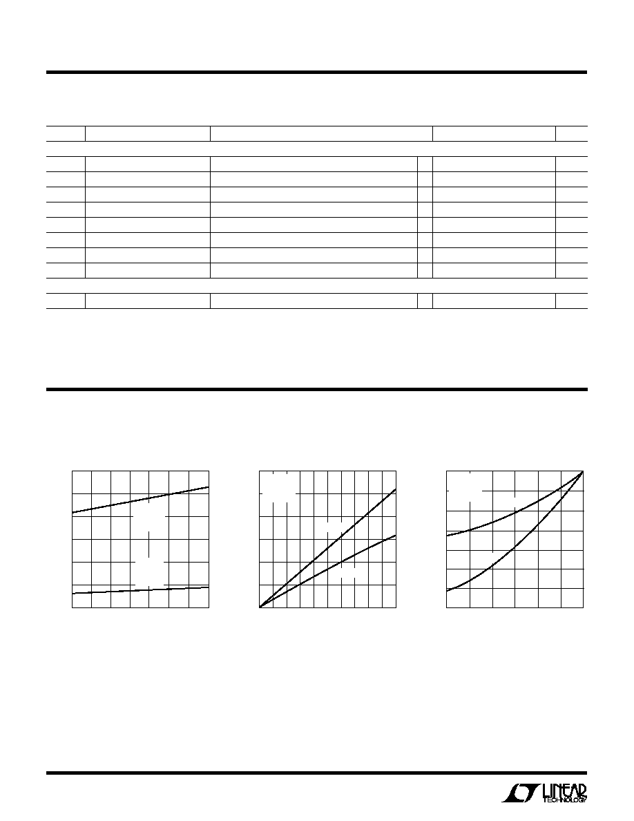
vs Output Current
TEMPERATURE (°C)
0
ON-RESISTANCE (
)
200
250
300
30
50
LTC1390 · G01
150
100
10
20
40
60
70
50
0
V
+
= 3V
V
= 0V
V
S
= 1.2V
V
+
= 5V
V
= 5V
V
S
= 0V
ON-Resistance vs Temperature
OUTPUT VOLTAGE (V)
2.0
3
2
1
3.5
4.5
LTC1390 · G03
4
5
2.5
3.0
4.0
5.0
6
7
OUTPUT CURRENT (mA)
0
T
A
= 25
°
C
V
+
= 5V
V
= 5V
DATA 2
DATA 1
OUTPUT VOLTAGE (V)
0
OUTPUT CURRENT (mA)
2
4
6
1
3
5
0.2
0.4
0.6
0.8
LTC1390 · G02
1.0
0.1
0
0.3
0.5
0.7
0.9
T
A
= 25
°
C
V
+
= 5V
V
= 5V
DATA 1
DATA 2
Driver Output Low Voltage
vs Output Current
5
LTC1390
PI
N
FU
N
CTIO
N
S
U
U
U
S0 to S7 (Pins 1 to 8): Analog Multiplexer Inputs/Analog
Demultiplexer Outputs.
GND (Pin 9): Digital Ground. Connect to system ground.
CLK (Pin 10): System Clock (TTL/CMOS Compatible). The
clock synchronizes the channel selection bits and the
serial data transfer from Data 1 to Data 2.
CS (Pin 11): Chip Select Input (TTL/CMOS Compatible). A
logic high on this input enables LTC1390 to read in the
channel selection bits and allow data transfer from Data 1
to Data 2. A logic low enables the desired channel for
analog signal transmission and allows data transfer from
Data 2 to Data 1.
Data 1 (Pin 12): Bidirectional Digital Input/Output (TTL/
CMOS Compatible). Input for the channel selection bits.
Data 2 (Pin 13): Bidirectional Digital Input/Output (TTL/
CMOS Compatible).
V
(Pin 14): Negative Supply.
D (Pin 15): Analog Multiplexer Output/Analog
Demultiplexer Input.
V
+
(Pin 16): Positive Supply.
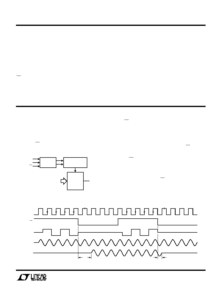
Figure 2: Multiplexer Operation
ANY
ANALOG
INPUTS
D
DATA 1
EN = HIGH
B2
B1
B0
EN = LOW
B2
B1
B0
LTC1390 · F02
CLK
CS
t
ON
t
OFF
APPLICATIO S I FOR ATIO
U
U
W
U
When CS is high, the input data on the Data 1 pin is latched
into the 4-bit shift register on each rising clock edge. The
input data consists of an "EN" bit and a string of three bits
for channel selection. If "EN" bit is logic high as illustrated
in the first input data sequence, it enables the selected
channel. To ensure correct operation, the CS must be
pulled low before the next rising clock edge.
Once the CS is pulled low, all channels are simultaneously
switched off to ensure a break-before-make interval. After
a delay of t
ON
, the selected channel is switched on allowing
signal transmission. The selected channel remains on
until the next falling edge of CS, and after a delay of t
OFF
,
it terminates the analog signal transmission and subse-
quently allows the selection of the next channel. If "EN" bit
is logic low, as illustrated in the second data sequence, it
disables all channels and there will be no analog signal
Multiplexer Operation
Figure 1 shows the block diagram of the components
within the LTC1390 required for MUX operation. The
LTC1390 uses Data 1 to select its 8 channels and a chip
select input CS to switch on the selected channel as shown
in Figure 2.
4-BIT SHIFT
REGISTER
CLK
DATA 1
CS
CONTROL
LOGIC
MUX
BLOCK
ANALOG
INPUT
ANALOG
OUTPUT
LTC1390 · F01
Figure 1: Simplified Block Diagram of the MUX Operation