/home/web/doc/html/liner/177744
1
LTC1427-50
Micropower, 10-Bit Current
Output DAC with SMBus
Serial Interface
1
2
3
4
8
7
6
5
1427 TA02
C1
1
µ
F
1
µ
F
1
2
5
6
4
3
4700pF
V
CC
3.3V
V
OUT
*
*V
OUT
= 12.7V TO 24V IN 11mV STEPS
15mA (2 CELLS)
35mA ( 3 CELLS)
L1 = 10
µ
H SUMIDA CD43
MURATA-ERIE LQH3C
OR COILCRAFT DO1608
D1 =MBR0530
100k
D1
2 TO 4
CELLS
L1
LTC1427-50
R1
226k
1%
R2
12.1k
1%
SHDN
AD1
AD0
GND
V
CC
I
OUT
SCL
SDA
P1.2
P1.1
P1.0
V
IN
V
C
GND
LT1317
SW
FB
SHDN
SHDN
µ
PU
(e.g., 8051)
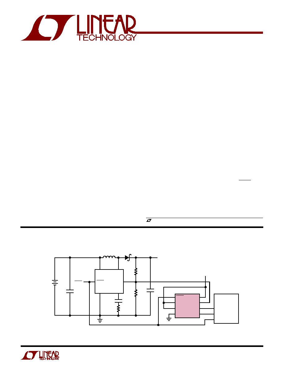
TYPICAL APPLICATIO
N
U
Digitally Controlled LCD Bias Generator
FEATURES
DESCRIPTIO
N
U
s
LCD Contrast and Backlight Brightness Control
s
Power Supply Voltage Adjustment
s
Battery Charger Voltage/Current Adjustment
s
GaAs FET Bias Adjustment
s
Trimmer Pot Elimination
The LTC
®
1427-50 is a micropower, 10-Bit current output
DAC with an output range of 0
µ
A to 50
µ
A. The DAC output is
guaranteed monotonic and DNL is less than 0.9LSB under all
operating conditions. Full-scale accuracy is
±
2.5% over
the commercial temperature range. The LTC1427-50 oper-
ates with power supply voltages from 2.7V to 5.5V and the
DAC current source output can be biased from (V
CC
1.3V)
to 15V.
The LTC1427-50 communicates with external circuitry by
using the SMBus serial interface. It acts as an SMBus slave
device using one of four selectable SMBus addresses set by
the two address pins AD0 and AD1 .
On power-up, the DAC output assumes midrange or zero
scale, depending on the logic state of the two address pins.
The LTC1427-50 can be shut down through the SHDN pin or
by setting the SHDN bit = 1 in the SMBus command byte.
Digital data for the DAC output is retained internally and the
supply current drops to 10
µ
A typically when in shutdown.
The LTC1427-50 is available in an 8-pin SO package.
APPLICATIO
N
S
U
s
Precision 50
µ
A,
±
1.5% Initial Full-Scale Output
Current,
±
2.5% Over Temperature
s
Wide Output Voltage DC Compliance: 15V to
(V
CC
1.3V)
s
Wide Supply Range: 2.7V
V
CC
5.5V
s
Supply Current in Shutdown: 10
µ
A Typ
s
Low Supply Current: 115
µ
A Typ
s
Available in 8-Pin SO
s
SMBus Serial Interface
s
Four Selectable SMBus Addresses
s
DAC Powers Up at Zero or Midscale
s
DAC Contents Are Retained in Shutdown
, LTC and LT are registered trademarks of Linear Technology Corporation.
2
LTC1427-50
ABSOLUTE
M
AXI
M
U
M
RATINGS
W
W
W
U
PACKAGE/ORDER I
N
FOR
M
ATIO
N
W
U
U
ORDER PART
NUMBER
ELECTRICAL CHARACTERISTICS
T
A
= operating temperature range unless otherwise specified.
SYMBOL
PARAMETER
CONDITIONS
MIN
TYP
MAX
UNITS
V
CC
Supply Voltage
q
2.7
5.5
V
I
CC
Supply Current
V
SHDN
= V
SCL
= V
SDA
= V
CC
= 3.3V
q
115
225
µ
A
V
SHDN
= 0V
q
10
25
µ
A
DAC Resolution
q
10
Bits
I
FS
DAC Full-Scale Current
V
CC
= 3.3V, V(I
OUT
) = 0V
49.25
50
50.75
µ
A
q
48.75
50
51.25
µ
A
I
ZS
DAC Zero-Scale Current
V
CC
= 3.3V, V(I
OUT
) = 0V
q
±
0.1
±
200
nA
DNL
DAC Differential Nonlinearity
V
CC
= 3.3V, Monotonicity Guaranteed, V(I
OUT
) = 0V
q
±
0.15
±
0.9
LSB
Supply Voltage Rejection
V
CC
= 2.7V to 5.5V, V(I
OUT
) = 0V
q
±
8
LSB
Output Voltage Rejection
V
CC
= 3.3V, Full-Scale Current, 15V
V(I
OUT
)
2V
q
±
5
LSB
I
IN
Logic Input Current
0V
V
IN
V
CC
q
±
1
µ
A
V
IH
High Level Input Voltage
AD0, AD1
q
V
CC
0.3
V
SHDN
q
2.4
V
SCL, SDA
q
1.4
V
V
IL
Low Level Input Voltage
SHDN, AD0, AD1
q
0.8
V
SCL, SDA
q
0.6
V
V
OL
Low Level Output Voltage
I
OUT
= 3mA, SDA Only
q
0.4
V
Consult factory for Industrial and Military grade parts.
T
JMAX
= 125
°
C,
JA
= 190
°
C/ W
TOP VIEW
V
CC
I
OUT
SCL
SDA
SHDN
AD1
AD0
GND
S8 PACKAGE
8-LEAD PLASTIC SO
1
2
3
4
8
7
6
5
S8 PART MARKING
LTC1427CS8-50
14275
(Note 1)
Total Supply Voltage (V
CC
) ........................................ 7V
Input Voltage (All Inputs)............. 0.3V to (V
CC
+ 0.3V)
DAC Output Voltage ...................... 15V to (V
CC
+ 0.3V)
DAC Output Short-Circuit Duration .................. Indefinite
Operating Ambient Temperature Range ....... 0
°
C to 70
°
C
Junction Temperature .......................................... 125
°
C
Storage Temperature Range ................. 65
°
C to 150
°
C
Lead Temperature (Soldering, 10 sec.)................. 300
°
C
3
LTC1427-50
RECO
E
DED OPERATI
G CO DITIO
S
U
U
U
U
W
W
TYPICAL PERFOR
M
A
N
CE CHARACTERISTICS
U
W
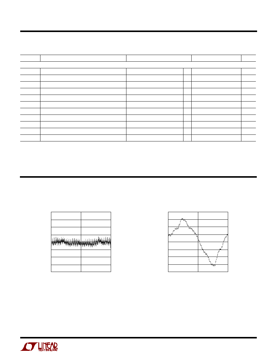
CODE
0
INL (LSB)
512
1024
1247 G02
6
4
2
0
2
4
6
8
10
INL vs Code
CODE
0
DNL (LSB)
512
1024
1247 G01
1.0
0.5
0
0.5
1.0
DNL vs Code
V
CC
= 3.3V, T
A
= operating temperature range unless otherwise specified.
Note 2: All values are referenced to V
IH
and V
IL
levels.
Note 3: These parameters are guaranteed by design and are not tested.
Refer to the Timing Diagrams for additional information.
SYMBOL
PARAMETER
CONDITIONS
MIN
TYP
MAX
UNITS
SMBus Timing (Notes 2, 3)
f
SMB
SMB Operating Frequency
q
10
100
kHz
t
BUF
Bus Free Time Between Stop and Start Condition
q
4.7
µ
s
t
HD:STA
Hold Time After (Repeated) Start Condition
q
4.0
µ
s
t
SU:STA
Repeated Start Condition Setup Time
q
4.7
µ
s
t
SU:STO
Stop Condition Setup Time
q
4.0
µ
s
t
HD:DAT
Data Hold Time
q
300
ns
t
SU:DAT
Data Setup Time
q
250
ns
t
LOW
Clock Low Period
q
4.7
µ
s
t
HIGH
Clock High Period
q
4.0
50
µ
s
t
f
Clock/Data Fall Time
q
300
ns
t
r
Clock/Data Rise Time
q
1000
ns
The
q
denotes specifications that apply over the full operating temperature
range.
Note 1: Absolute Maximum Ratings are those beyond which the life of the
device may be impaired.
4
LTC1427-50
TYPICAL PERFOR
M
A
N
CE CHARACTERISTICS
U
W
Zero-Scale Current vs
Temperature
TEMPERATURE (
°
C)
OUTPUT CURRENT (
µ
A)
1427 G03
0.02
0
0.02
0.04
0.06
0.08
0.10
0.12
0.14
0.16
0.18
25
50
75
125
100
150
50 25
0
V (I
OUT
) = 0V
TEMPERATURE (
°
C)
1427 G04
OUTPUT CURRENT (
µ
A)
52
51
50
49
48
25
50
75
125
100
150
50 25
0
V(I
OUT
) = 0V
Full-Scale Current vs
Temperature
Bias Voltage Rejection
(Zero-Scale Current)
I
OUT
BIAS VOLTAGE (V)
15
4
2
0
2
4
0
3
1427 G05
12
9
6
3
6
ZERO-SCALE OUTPUT CURRENT (nA)
T
A
= 25
°
C
V
CC
= 3.3V
I
OUT
BIAS VOLTAGE (V)
15
1.0
0.5
0
0.5
1.0
0
3
1427 G06
12
9
6
3
6
FULL-SCALE OUTPUT ERROR (LSB)
T
A
= 25
°
C
V
CC
= 3.3V
SUPPLY VOLTAGE (V)
0
2
1
0
1
2
5
6
1427 G07
1
2
3
4
7
FULL-SCALE OUTPUT ERROR (LSB)
T
A
= 25
°
C
V(I
OUT
) = 0V
Supply Current vs Temperature
Shutdown Current vs Temperature
Bias Voltage Rejection
(Full-Scale Current)
Supply Voltage Rejection
TEMPERATURE (
°
C)
SHUTDOWN CURRENT (
µ
A)
1527 G09
20
15
10
5
0
25
50
75
125
100
150
50 25
0
V
CC
= 5.5V
V
CC
= 2.7V
V
CC
= 3.3V
TEMPERATURE (
°
C)
SUPPLY CURRENT (
µ
A)
1527 G08
200
150
100
50
0
25
50
75
125
100
150
50 25
0
V
CC
= 5.5V
V
CC
= 2.7V
V
CC
= 3.3V
5
LTC1427-50
PI
N
FU
N
CTIO
N
S
U
U
U
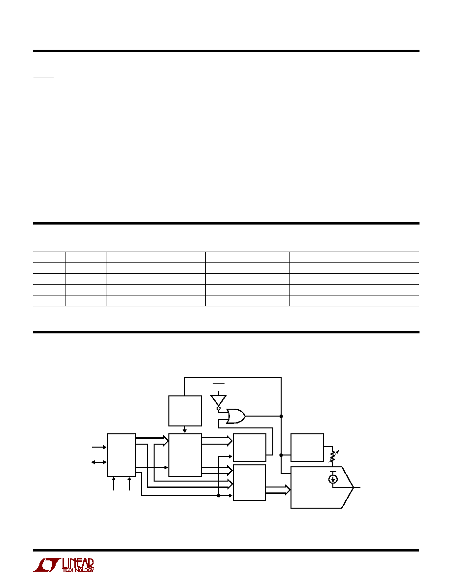
SHDN (Pin 1): Shutdown. A logic low puts the chip into
shutdown mode. In shutdown, the digital settings for the
DAC are retained. On release from shutdown, the previ-
ously programmed value for I
OUT
is reinstated.
AD1, AD0 (Pins 2, 3): Address Selection Pins. Tie these
two pins to either V
CC
or GND to select one of four SMBus
addresses to which the LTC1427-50 will respond.
GND (Pin 4): Ground. Ground should be tied directly to a
ground plane.
SDA (Pin 5): SMBus Bidirectional Data Input/Digital Out-
put. This pin is an open-drain output and requires a pull-
up resistor or current source to V
CC
. Data is shifted into the
SDA pin and acknowledged by the SDA pin.
SCL (Pin 6): SMBus Clock Input. Data is shifted into the
SDA pin at the rising edges of the SCL clock during data
transfer.
I
OUT
(Pin 7): DAC Current Output.
V
CC
(Pin 8): Voltage Supply. This supply must be kept free
from noise and ripple by bypassing directly to the ground
plane.
SMBUS
INTERFACE
3-BIT
LATCH
REGISTER A
SCL
SDA
AD0
AD1
EN1
10-BIT
LATCH
10-BIT
CURRENT
DAC
1-BIT LATCH
VOLTAGE
REFERENCE
REGISTER C
REGISTER B
3
1
2
10
8
EN2
EN2
POWER-ON
RESET
SHDN
SHDN
SD
SD
1427 BD
R
ADJ
I
OUT
SD
BLOCK DIAGRA
M
W
FU CTIO TABLES
U
U
AD1
AD0
SMBus Address Location
DAC Power-Up Value
Application
L
L
0101101
Zero-Scale
CCFL Backlight Control
L
H
0101111
Zero-Scale
General Purpose
H
L
0101110
Zero-Scale
General Purpose
H
H
0101100
Midscale
LCD Contrast Control