Äîêóìåíòàöèÿ è îïèñàíèÿ www.docs.chipfind.ru
1
LTC1428-50
Micropower 8-Bit Current
Sink Output D/A Converter
FEATURES
DESCRIPTIO
N
U
The LTC
®
1428-50 is a micropower 8-bit current sink
output D/A converter (DAC) with an output range of 0
µ
A to
50
µ
A. In 3.3V or 5V systems, the DAC I
OUT
pin can be
biased from 2V to 10V. Supply current is only 130
µ
A.
Shutdown mode drops the supply current to 0.2
µ
A.
The LTC1428-50 communicates with external circuitry by
using one of three interface modes: standard 3-wire serial
mode or one of two pulse modes. Upon power-up, the
internal counter resets to 10000000B, the DAC output
assumes midrange and the chip configures to 3-wire or
pulse mode depending on the CS signal level.
In 3-wire mode, the system MPU can serially transfer
8-bit data to and from the LTC1428-50. In pulse mode, the
upper six bits of the DAC output program for increment-
only (1-wire interface) or increment/decrement (2-wire
interface) operation depending on the D
IN
signal level. In
increment-only mode, the counter rolls over and sets the
DAC to zero if the counter increases beyond full scale. In
increment/decrement mode, the counter stops
incrementing at full scale, stops decrementing at zero
scale and does not roll over.
LTC1428-50 is available in an 8-pin SO package.
APPLICATIO
N
S
U
s
LCD Contrast Control
s
Backlight Brightness Control
s
Power Supply Voltage Adjustment
s
Battery Charger Voltage/Current Adjustment
s
GaAs FET Bias Adjustment
s
Trimmer Pot Elimination
s
Precision Full-Scale DAC Output Current
at 25
°
C: 50
µ
A
±
3%
s
Wide Output Voltage DC Compliance: 2V to 10V
s
Wide Supply Range: 3V
V
CC
6.5V
s
Supply Current in Shutdown: 0.2
µ
A
s
Low Supply Current: 130
µ
A
s
Available in 8-Pin SO
s
Triple Mode
TM
Interface
1. Standard 3-Wire Mode
2. 1-Wire Pulse Mode Interface: Increment-Only
3. 2-Wire Pulse Mode Interface: Increment/Decrement
s
DAC Value Read Back Capability in 3-Wire Mode
s
DAC Powers Up at Midrange
s
DAC Contents Are Retained in Shutdown
, LTC and LT are registered trademarks of Linear Technology Corporation.
Triple Mode is a trademark of Linear Technology Corporation.
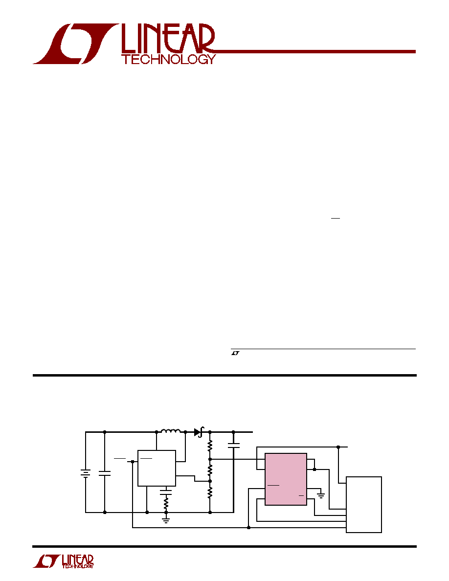
TYPICAL APPLICATIO
N
U
1
2
8
7
D
OUT
D
IN
I
OUT
V
CC
SHDN
CLK
LTC1428-50
GND
CS
1
µ
F
2
CELLS
1428-50 TA01
V
OUT
15.75V TO 27.75V IN STEPS OF 47mV
15mA FROM 2 CELLS
R1
240k
3
4
6
5
C1
0.1
µ
F
LT
®
1307
L1
L1: 4.7
µ
H MURATA-ERIE LQH3C
D1: MBR0530 OR 1N4148
D1
V
IN
FB
V
C
GND
SW
SHDN
SHDN
R2
22k
R3
22k
100k
MPU
(e.g., 8051)
P1.3
P1.2
P1.1
P1.0
V
CC
5V
4700pF
Digitally Controlled LCD Bias Generator (Standard 3-Wire Mode)
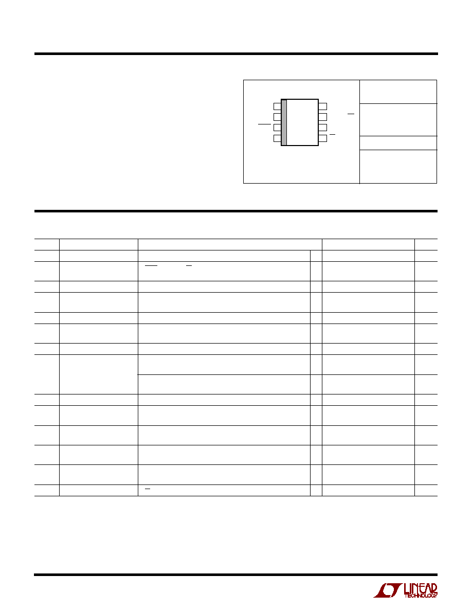
2
LTC1428-50
ABSOLUTE
M
AXI
M
U
M
RATINGS
W
W
W
U
PACKAGE/ORDER I
N
FOR
M
ATIO
N
W
U
U
(Note 1)
Supply Voltage (V
CC
) ................................................ 7V
Input Voltage (All Inputs)............ 0.3V to (V
CC
+ 0.3V)
Output Voltage
I
OUT
...................................................... 0.3V to 10V
D
OUT
....................................... 0.3V to (V
CC
+ 0.3V)
Short-Circuit Duration (All Outputs) ............... Indefinite
Operating Temperature Range .................... 0
°
C to 70
°
C
Storage Temperature Range ................. 65
°
C to 150
°
C
Lead Temperature (Soldering, 10 sec).................. 300
°
C
ORDER PART
NUMBER
V
CC
= 3.3V, T
A
= 25
°
C, unless otherwise specified.
ELECTRICAL CHARACTERISTICS
LTC1428CS8-50
Consult factory for Industrial and Military grade parts.
14285
S8 PART MARKING
T
JMAX
= 125
°
C,
JA
= 130
°
C/ W
1
2
3
4
8
7
6
5
TOP VIEW
D
OUT
D
IN
(UP/DN)
GND
CS
I
OUT
V
CC
SHDN
CLK
S8 PACKAGE
8-LEAD PLASTIC SO
SYMBOL PARAMETER
CONDITIONS
MIN
TYP
MAX
UNITS
V
CC
q
3.0
6.5
V
I
CC
Supply Current
V
SHDN
= V
DIN
= V
CS
= V
CC
, V
CLK
= 0V, D
OUT
= NC, I
OUT
= NC
q
130
225
µ
A
Shutdown
q
0.2
10
µ
A
DAC Resolution
8
Bits
DAC Full-Scale Current
I
OUT
Bias Voltage = 2.5V
48.5
50
51.5
µ
A
q
47.5
50
52.5
µ
A
DAC Zero-Scale Current
I
OUT
Bias Voltage = 2.5V
q
200
nA
DAC Differential
Monotonicity Guaranteed, No Missing Codes
q
±
0.9
LSB
Nonlinearity
Supply Voltage Rejection
V
CC
= 3V to 6.5V, Full Scale Current, I
OUT
Bias Voltage = 2.5V
q
±
1
±
4
LSB
Output Voltage Rejection
V
CC
= 5V, Full Scale Current,
q
±
1
LSB
2V
V(I
OUT
)
3V
V
CC
= 5V, Full Scale Current,
q
±
1
±
4
LSB
3V
V(I
OUT
)
10V
Logic Input Current
0V
V
IN
V
CC
q
±
1
µ
A
V
IH
High Level Input Voltage
V
CC
= 5V
q
2.0
V
V
CC
= 3.3V
q
1.9
V
V
IL
Low Level Input Voltage
V
CC
= 5V
q
0.80
V
V
CC
= 3.3V
q
0.45
V
V
OH
High Level Output Voltage
V
CC
= 5V, I
O
= 400
µ
A
q
2.4
V
V
CC
= 3.3V, I
O
= 400
µ
A
q
2.1
V
V
OL
Low Level Output Voltage
V
CC
= 5V, I
O
= 2mA
q
0.4
V
V
CC
= 3.3V, I
O
= 1mA
q
0.4
V
I
OZ
Three-State Output Leakage
V
CS
= V
CC
q
±
5
µ
A
3
LTC1428-50
V
CC
= 5V, unless otherwise specified. (Notes 2, 3)
RECO
E
DED OPERATI
G CO DITIO
S
U
U
U
U
W
W
TYPICAL PERFOR
M
A
N
CE CHARACTERISTICS
U
W
The
q
denotes specifications which apply over the full operating
temperature range.
Note 1: Absolute Maximum Ratings are those values beyond which the life
of the device may be impaired.
Note 2: Timing for all input signals is measured at 0.8V for a High-to-Low
transition and at 2V for a Low-to-High transition.
Note 3: Timing specifications are guaranteed by design but not tested.
Note 4: This is the minimum time required for valid data transfer.
CODE
0
1.0
DNL (LSB)
0.8
0.4
0.2
0
1.0
0.4
64
128
160
1428-50 G01
0.6
0.6
0.8
0.2
32
96
192 224
256
V
CC
= 3.3V
V(I
OUT
) = 2.5V
T
A
= 25
°
C
DNL vs Code
Supply Voltage Rejection
INL vs Code
CODE
0
INL (LSB)
1.0
0.8
0.6
0.4
0.2
0
0.2
0.4
0.6
0.8
1.0
64
128
160
1428-50 G02
32
96
192 224
256
V
CC
= 3.3V
V(I
OUT
) = 2.5V
T
A
= 25
°
C
SYMBOL PARAMETER
CONDITIONS
MIN
TYP
MAX
UNITS
Serial Interface
f
CLK
Clock Frequency
q
2
MHz
t
CKS
Setup Time, CLK
Before CS
q
150
ns
t
CSS
Setup Time, CS
Before CLK
q
400
ns
t
DV
CS
to D
OUT
Valid
See Test Circuits
q
150
ns
t
DS
D
IN
Setup Time Before CLK
q
150
ns
t
DH
D
IN
Hold Time After CLK
q
150
ns
t
DO
CLK
to D
OUT
Valid
See Test Circuits
q
150
ns
t
CKHI
CLK High Time
q
200
ns
t
CKLO
CLK Low Time
q
250
ns
t
CSH
CLK
Before CS
q
150
ns
t
DZ
CS
to D
OUT
in Hi-Z
See Test Circuits
q
400
ns
t
CKH
CS
Before CLK
q
400
ns
t
CSLO
CS Low Time
f
CLK
= 2MHz (Note 4)
q
4550
ns
V
CLK
= 0V
400
ns
t
CSHI
CS High Time
q
400
ns
SUPPLY VOLTAGE (V)
1
FULL-SCALE OUTPUT CURRENT (LSB)
0.5
0
0.5
4
6
1428-50 G03
1.0
1.5
2.0
2
3
5
1.0
1.5
2.0
7
V(I
OUT
) = 2.5V
T
A
= 25
°
C
4
LTC1428-50
TYPICAL PERFOR
M
A
N
CE CHARACTERISTICS
U
W
PI
N
FU
N
CTIO
N
S
U
U
U
I
OUT
(Pin 1): DAC Current Sink Output. In 3.3V or 5V
systems, the DAC I
OUT
pin can be biased from 2V to 10V.
V
CC
(Pin 2): Voltage Supply (3V
V
CC
6.5V). This supply
must be kept free from noise and ripple by bypassing
directly to a ground plane.
SHDN (Pin 3): Shutdown. A logic low puts the chip
into shutdown mode. The digital setting for the DAC is
retained.
CLK (Pin 4): Shift Clock. This clock synchronizes the serial
data and has a Schmitt trigger input.
CS (Pin 5): Chip Select Input. In 3-wire mode, a logic low
enables the LTC1428-50. Upon power-up, a logic high
puts the chip into pulse mode. If CS ever goes low, the chip
is configured into 3-wire mode until V
CC
is reset.
GND (Pin 6): Ground. Ground should be tied directly to a
ground plane.
D
IN
(UP/DN)(Pin 7): Data Input. In 3-wire mode, the DAC
data is shifted into D
IN
. In pulse mode, upon power-up a
logic high puts the counter into increment-only mode. If
D
IN
ever goes low, the counter is configured in increment/
decrement mode until V
CC
is reset.
D
OUT
(Pin 8): Data Output. In 3-wire mode, on every
conversion D
OUT
serially outputs the previous 8-bit DAC
data. In pulse mode, D
OUT
is three-stated.
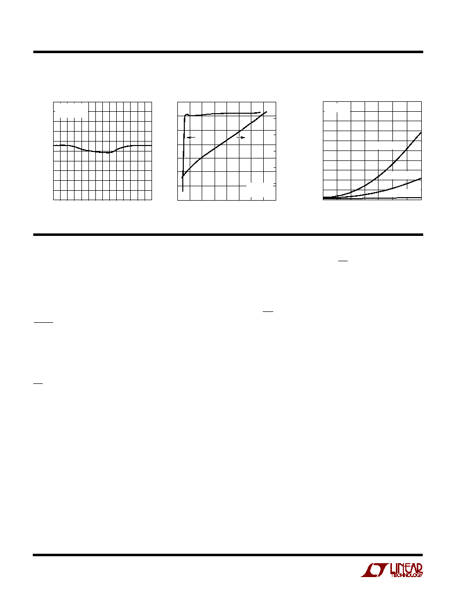
Temperature Variation
TEMPERATURE (
°
C)
55
FULL-SCALE OUTPUT CURRENT (
µ
A)
50.5
51.5
52.5
65
1428-50 G04
49.5
48.5
47.5
25
5
35
95
125
155
V
CC
= 3.3V
V(I
OUT
) = 2.5V
TEMPERATURE (
°
C)
0
0
ZERO-SCALE CURRENT (nA)
2
6
8
10
20
14
20
40
50
1428-50 G06
4
16
18
12
10
30
60
70
V
CC
= 3.3V
V(I
OUT
) = 10V
V(I
OUT
) = 5V
V(I
OUT
) = 2.5V
Bias Voltage Rejection
I
OUT
BIAS VOLTAGE (V)
0
FULL-SCALE OUTPUT CURRENT (LSB)
ZERO-SCALE OUTPUT CURRENT (LSB)
4
2
0
12
1428-50 G05
6
8
4
8
2
14
6
10
16
10
12
2
0.03
0.04
0.05
0.02
0.01
0
0.06
V
CC
= 3.3V
T
A
= 25
°
C
Zero-Scale I
OUT
vs Temperature
5
LTC1428-50
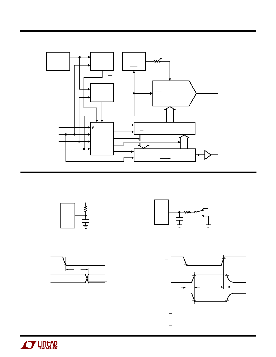
BLOCK DIAGRA
W
TEST CIRCUITS
Load Circuit for t
DO
3k
100pF
1428-50 TC01
1.4V
D
OUT
Load Circuit for t
DZ,
t
DV
3k
100pF
1428-50 TC02
5V t
DZ
WAVEFORM 2, t
DV
t
DZ
WAVEFORM 1
D
OUT
Voltage Waveforms for t
DO
0.8V
0.4V
2.4V
1428-50 TC03
D
OUT
CLK
t
DO
Voltage Waveforms for t
DZ
, t
DV
1428-50 TC04
0.8V
CS
D
OUT
WAVEFORM 1
(SEE NOTE 1)
D
OUT
WAVEFORM 2
(SEE NOTE 2)
2.4V
NOTE 1: WAVEFORM 1 IS FOR AN OUTPUT WITH INTERNAL
CONDITIONS SUCH THAT THE OUTPUT IS HIGH UNLESS
DISABLED BY CS
NOTE 2: WAVEFORM 2 IS FOR AN OUTPUT WITH INTERNAL
CONDITIONS SUCH THAT THE OUTPUT IS LOW UNLESS
DISABLED BY CS
2.0V
90%
10%
0.4V
t
DV
t
DZ
LATCH
AND
LOGIC
LATCH
AND
LOGIC
8-BIT
CURRENT
DAC
CLK
SHDN
CLK
1428-50 BD
D
OUT
(LSB)
Q9
UP/DN
8-BIT REGISTER/COUNTER
I
OUT
D
OUT
8
8
8
9-BIT SHIFT REGISTER
VOLTAGE
REFERENCE
UP ONLY/
UP/DN
MODE SELECT
0 = PULSE
1 = SPI
POWER-ON
RESET
CONTROL
LOGIC
CLK
D
IN
CS
SHDN
SHDN