1
LTC1517-5
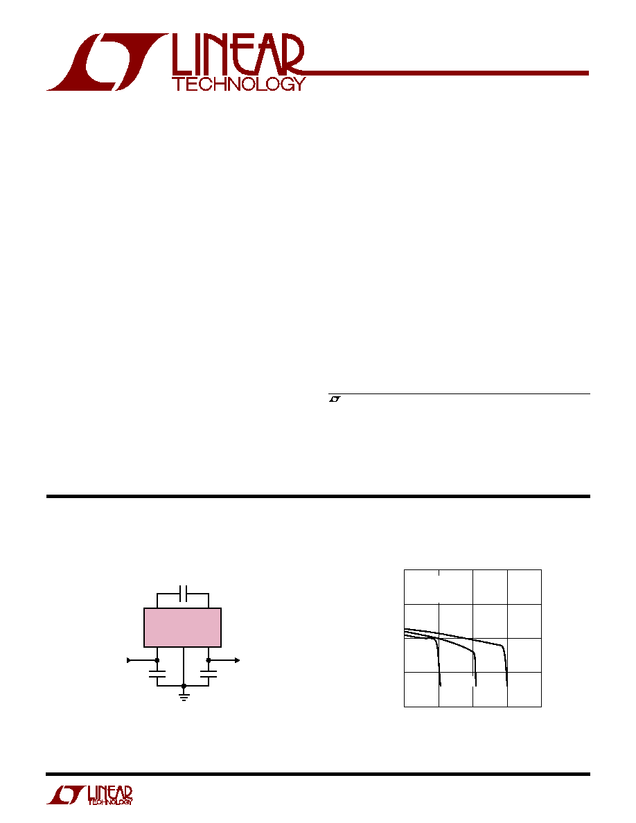
TYPICAL APPLICATIO
N
U
Micropower, Regulated
5V Charge Pump in a
5-Pin SOT-23 Package
s
Ultralow Power: I
CC
= 6
Ķ
A Typ
s
Short-Circuit/Thermal Protected
s
5V
Ī
4% Regulated Output
s
V
IN
Range: 2.7V to 5V
s
Output Current: 10mA (V
IN
2.7V)
20mA (V
IN
3V)
s
No Inductors
s
Ultrasmall Application Circuit (0.045in
2
)
s
800kHz Switching Frequency
s
Available in 5-Pin SOT-23
FEATURES
DESCRIPTIO
N
U
The LTC
ģ
1517-5 is a micropower charge pump DC/DC
converter that produces a regulated 5V output. The input
voltage range is 2.7V to 5V. Extremely low operating current
(typically 6
Ķ
A with no load) and low external parts count (one
0.1
Ķ
F flying capacitor and two small bypass capacitors at V
IN
and V
OUT
) make the part ideally suited for small, light load
battery-powered applications. The total printed circuit board
area of the application circuit shown below is only 0.045in
2
.
The part operates as a Burst Mode
TM
switched-capacitor
voltage doubler to produce a regulated output. The part has
thermal shutdown capability and can survive a continuous
short circuit from V
OUT
to GND. The device is available in a
5-pin SOT-23 package.
, LTC and LT are registered trademarks of Linear Technology Corporation.
Burst Mode is a trademark of Linear Technology Corporation.
OUTPUT CURRENT (mA)
0
OUTPUT VOLTAGE (V)
5.0
5.1
80
1517 TA02
4.9
4.8
20
40
60
5.2
V
IN
= 3.3V
V
IN
= 3V
V
IN
= 2.7V
T
A
= 25
į
C
C1 = 0.1
Ķ
F
C
OUT
= 6.8
Ķ
F
Typical Output Voltage vs Output Current
3.3
Ķ
F
1517 TA01
1
2
3
4
5
0.1
Ķ
F
6.8
Ķ
F
V
OUT
= 5V
Ī
4%
I
OUT
= 10mA (V
IN
2.7V)
I
OUT
= 20mA (V
IN
3V)
V
IN
2.7V TO 5V
V
IN
GND
LTC1517-5
V
OUT
C1
+
C1
≠
s
Cellular Telephones
s
Battery-Operated Equipment
s
Local Power Supplies
s
Handheld Instruments
s
PCMCIA Supplies
APPLICATIO
N
S
U

2
LTC1517-5
ABSOLUTE
M
AXI
M
U
M
RATINGS
W
W
W
U
PACKAGE/ORDER I
N
FOR
M
ATIO
N
W
U
U
ORDER PART
NUMBER
(Note 1)
V
IN
to GND ...................................................≠ 0.3V to 6V
V
OUT
to GND ................................................≠ 0.3V to 6V
V
OUT
Short-Circuit Duration ............................. Indefinite
Operating Temperature Range:
Commercial (Note 2) .............................. 0
į
C to 70
į
C
Storage Temperature Range ................. ≠ 65
į
C to 150
į
C
Lead Temperature (Soldering, 10 sec) .................. 300
į
C
S5 PART MARKING
T
JMAX
= 125
į
C,
JA
= 256
į
C/ W
C1
≠
5
C1
+
1
2
3
V
IN
TOP VIEW
S5 PACKAGE
5-LEAD PLASTIC SOT-23
V
OUT
GND
4
Consult factory for Industrial and Military grade parts and for -3 and -3.3
version availability.
SYMBOL
PARAMETER
CONDITIONS
MIN
TYP
MAX
UNITS
V
IN
Operating Input Voltage
q
2.7
5
V
V
OUT
Output Voltage
2.7V
V
IN
5V, I
OUT
10mA
q
4.8
5.0
5.2
V
3V
V
IN
5V, I
OUT
20mA
q
4.8
5.0
5.2
V
I
CC
Input Supply Current
2.7V
V
IN
5V, I
OUT
= 0
q
6
15
Ķ
A
V
OUT
Ripple
V
IN
= 3V, I
OUT
= 20mA, C
OUT
= 6.8
Ķ
F
75
mV
P-P
f
OSC
Oscillator Frequency
800
kHz
t
ON
V
OUT
Turn-On Time
V
IN
= 3V
1
ms
V
IN
= 2.7V to 5V, C1 = 0.1
Ķ
F, C
IN
= 3.3
Ķ
F, C
OUT
= 6.8
Ķ
F, T
MIN
to T
MAX
, unless otherwise noted.
ELECTRICAL CHARACTERISTICS
The
q
denotes specifications that apply over the full operating
temperature range.
Note 1: Absolute Maximum Ratings are those values beyond which the life
of the device may be impaired.
Note 2: Commercial grade parts are designed to operate over the
temperature range of ≠ 40
į
C to 85
į
C but are neither tested nor guaranteed
beyond 0
į
C to 70
į
C.
LTC1517CS5-5
LTCJ
3
LTC1517-5
TYPICAL PERFOR
M
A
N
CE CHARACTERISTICS
U
W
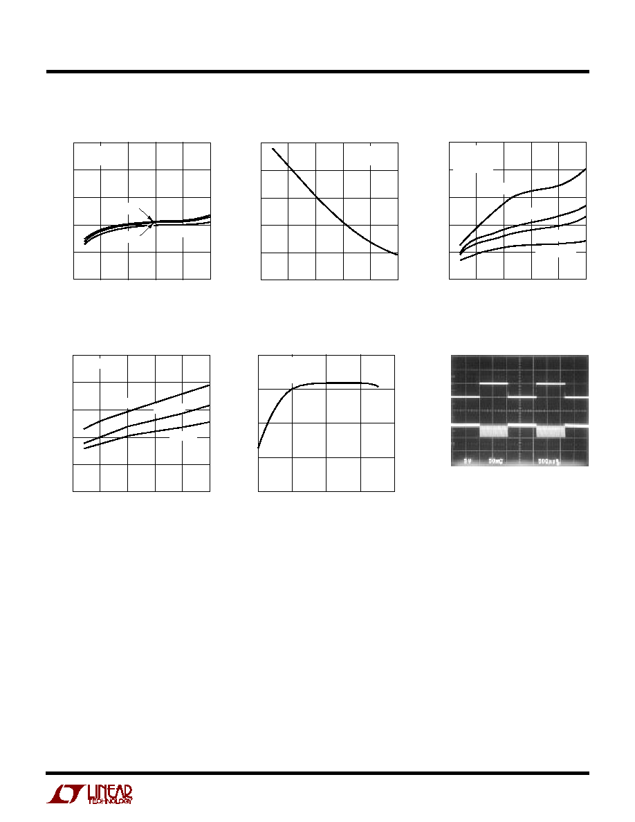
Output Ripple vs Input Voltage
INPUT VOLTAGE (V)
2.5
OUTPUT VOLTAGE (V)
5.05
5.10
5.15
4.5
1517-5 G01
5.00
4.95
4.90
3.0
3.5
4.0
5.0
I
OUT
= 10mA
C
OUT
= 10
Ķ
F
T
A
= 70
į
C
T
A
= 25
į
C
T
A
= 0
į
C
Output Voltage vs Input Voltage
INPUT VOLTAGE (V)
2.5
V
RIPPLE P-P
(mV) 150
200
250
4.5
1517-5 G03
100
50
0
3.0
3.5
4.0
5.0
I
OUT
= 10mA
C1 = 0.1
Ķ
F
T
A
= 25
į
C
C
OUT
= 6.8
Ķ
F
C
OUT
= 10
Ķ
F
C
OUT
= 22
Ķ
F
C
OUT
= 3.3
Ķ
F
INPUT VOLTAGE (V)
2.5
EFFICIENCY (%)
70
80
90
4.5
1517-5 G02
60
50
40
3.0
3.5
4.0
5.0
I
OUT
= 10mA
T
A
= 25
į
C
Efficiency vs Input Voltage
No Load Input Current
vs Input Voltage
INPUT VOLTAGE (V)
2.5
INPUT CURRENT (
Ķ
A)
7
8
9
4.5
1517-5 G04
6
5
4
3.0
3.5
4.0
5.0
I
OUT
= 0mA
T
A
= 70
į
C
T
A
= 25
į
C
T
A
= 0
į
C
OUTPUT CURRENT (mA)
50
60
70
80
90
EFFICIENCY (%)
100
1517-5 G05
0.01
0.1
1
10
V
IN
= 3V
SHDN = 0V
T
A
= 25
į
C
Efficiency vs Output Current
Load Transient Response
I
OUT
0mA to 10mA
10mA/DIV
V
OUT
AC COUPLED
50mV/DIV
V
IN
= 3V
500
Ķ
s/DIV
1517-5 G06
C
OUT
= 6.8
Ķ
F
4
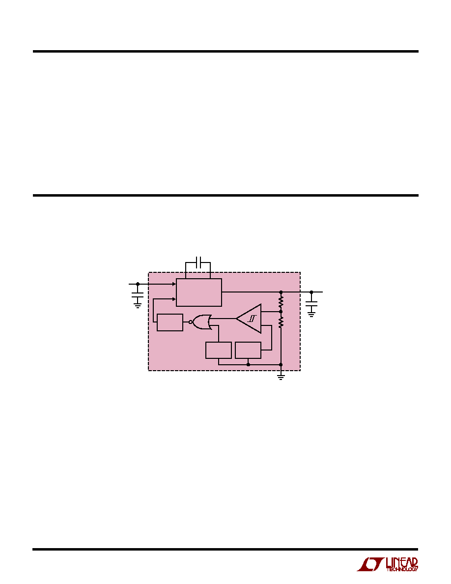
LTC1517-5
SI PLIFIED
W
BLOCK DIAGRA
W
1517 BD
C1
0.1
Ķ
F
V
IN
CHARGE PUMP
LTC1517-5
V
OUT
3.75M
1.25M
C
OUT
C
IN
C1
+
C1
≠
800kHz
OSC
THERMAL
SHDN
1.25V
REF
≠
+
V
IN
(Pin 1): Charge Pump Input Voltage. May be between
2.7V and 5V. V
IN
should be bypassed with a
3.3
Ķ
F low
ESR capacitor as close as possible to the pin for best
performance.
GND (Pin 2): Ground. Should be tied to a ground plane for
best performance.
PI
N
FU
N
CTIO
N
S
U
U
U
V
OUT
(Pin 3): Regulated Output Voltage. V
OUT
should be
bypassed with a
3.3
Ķ
F low ESR capacitor as close as
possible to the pin for best performance.
C1
+
(Pin 4): Charge Pump Flying Capacitor Positive
Terminal.
C1
≠
(Pin 5): Charge Pump Flying Capacitor Negative
Terminal.

5
LTC1517-5
APPLICATIO
N
S I
N
FOR
M
ATIO
N
W
U
U
U
Operation
The LTC1517-5 uses a switched-capacitor charge pump
to boost V
IN
to a 5V
Ī
4% regulated output. The part
achieves regulation by sensing the output voltage through
an internal resistor divider and enabling the charge pump
when the divided output droops below the comparator's
lower trip point (set by V
REF
). When the charge pump is
enabled, a 2-phase nonoverlapping clock controls the
internal charge pump switches. Flying capacitor C1 is
charged to V
IN
on phase one of the clock. On phase two of
the clock, C1 is stacked in series with V
IN
and connected
to V
OUT
through an internal switch. This sequence of
charging and discharging the flying capacitor occurs at a
free running frequency of 800kHz (typ) and continues until
the divided output voltage reaches the upper trip point of
the comparator. Once the output is back in regulation, the
charge pump is disabled. This method of bursting the
charge pump on and off enables the LTC1517-5 to achieve
high efficiency at extremely low output loads.
Capacitor Selection
For best performance, it is recommended that low ESR
capacitors be used for both C
IN
and C
OUT
to reduce noise
and ripple. The C
IN
and C
OUT
capacitors should be either
ceramic or tantalum and should be 3.3
Ķ
F or greater.
Ceramic capacitors will provide the smallest size and
lowest ESR for a given capacitance. If the input source
impedance is very low (< 0.5
), C
IN
may not be needed.
Ceramic capacitors are recommended for the flying ca-
pacitor C1 with values of 0.1
Ķ
F or 0.22
Ķ
F. Smaller value
flying capacitors may be used in low I
OUT
applications.
Output Ripple
Normal LTC1517-5 operation produces voltage ripple on
the V
OUT
pin. Output voltage ripple is required for the part
to regulate. Low frequency ripple exists due to the hyster-
esis in the sense comparator and propagation delays in the
charge pump enable/disable circuits. High frequency ripple
is also present mainly from the ESR (equivalent series
resistance) in the output capacitor. Typical output ripple
with V
IN
= 3V under maximum load is 100mV peak-to-peak
with a low ESR (< 0.5
) 3.3
Ķ
F output capacitor (minimum
recommended C
OUT
). For applications requiring V
IN
to
exceed 3.3V or for applications requiring < 100mV of
peak-to-peak ripple, a 6.8
Ķ
F to 10
Ķ
F C
OUT
capacitor is
recommended. Slight further decreases in output ripple
can be achieved by using C
OUT
capacitors larger than
10
Ķ
F.
Short-Circuit/Thermal Protection
During short-circuit conditions, the LTC1517-5 will draw
between 50mA and 200mA from V
IN
, causing a rise in
junction temperature. On-chip thermal shutdown circuitry
disables the charge pump once the junction temperature
exceeds approximately 160
į
C. The charge pump is
reenabled once the junction temperature drops to approxi-
mately 145
į
C. The LTC1517-5 will cycle in and out of
thermal shutdown indefinitely without latchup or damage
until the V
OUT
short is removed.

6
LTC1517-5
TYPICAL APPLICATIO
N
S
U
1
Ķ
F
1517 TA04a
1
2
3
4
5
0.1
Ķ
F
3.3
Ķ
F
1
Ķ
F
1
Ķ
F
1
Ķ
F
470
470
V
OUT
= 5V
I
OUT
= 1mA (V
IN
3.3V)
I
OUT
= 10mA (V
IN
3.6V)
V
RIPPLE
< 2mV
P-P
V
IN
3.3V TO 5V
V
IN
GND
LTC1517-5
V
OUT
C1
+
C1
≠
Q2
Q1, Q2: 2N3904
Q1
A
B
50mV/DIV
AC COUPLED
V
OUT
2mV/DIV
AC COUPLED
50
Ķ
s/DIV
V
IN
= 3.3V
I
OUT
= 1mA
1517-5 TA04b
Low Noise Boosted 5V Supply
Generating 5V and a Negative Supply
3.3
Ķ
F
1517 TA05
1
2
3
4
5
0.1
Ķ
F
0.1
Ķ
F
*
**
3.3k
V
OUT
= 5V
Ī
4%
I
OUT
= 10mA (2.7V
V
IN
5V)
I
OUT
= 20mA (3V
V
IN
5V)
≠ V
OUT
= ≠ 1.4V TO ≠ 3.5V
≠ I
OUT
= 0mA to 5mA
V
IN
2.7V TO 5V
V
IN
GND
LTC1517-5
V
OUT
C1
+
C1
≠
8.2k
470
3.3
Ķ
F
CENTRAL SEMICONDUCTOR CMPSH-35 DUAL SCHOTTKY
OPTIONAL CIRCUITRY FOR MAINTAINING ≠ V
OUT
WITH LOW
V
OUT
LOADS
Q1, Q2: 2N3904
*
**
3.3
Ķ
F
Q2
Q1
A
B
7
LTC1517-5
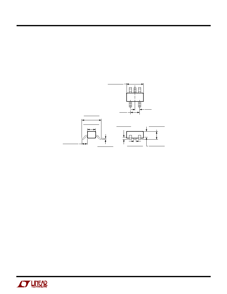
Dimensions in inches (millimeters) unless otherwise noted.
PACKAGE DESCRIPTIO
N
U
S5 Package
5-Lead Plastic SOT-23
(LTC DWG # 05-08-1633)
0.95
(0.037)
REF
1.50 ≠ 1.75
(0.059 ≠ 0.069)
0.10 ≠ 0.60
(0.004 ≠ 0.024)
REF
0.35 ≠ 0.50
(0.014 ≠ 0.020)
FIVE PLACES (NOTE 2)
S5 SOT-23 0797
2.80 ≠ 3.00
(0.110 ≠ 0.118)
(NOTE 3)
1.90
(0.074)
REF
0.90 ≠ 1.45
(0.035 ≠ 0.057)
0.90 ≠ 1.30
(0.035 ≠ 0.051)
0.00 ≠ 0.15
(0.00 ≠ 0.006)
0.09 ≠ 0.20
(0.004 ≠ 0.008)
(NOTE 2)
2.60 ≠ 3.00
(0.102 ≠ 0.118)
NOTE:
1. DIMENSIONS ARE IN MILLIMETERS
2. DIMENSIONS ARE INCLUSIVE OF PLATING
3. DIMENSIONS ARE EXCLUSIVE OF MOLD FLASH AND METAL BURR
4. MOLD FLASH SHALL NOT EXCEED 0.254mm
5. PACKAGE EIAJ REFERENCE IS SC-74A (EIAJ)
Information furnished by Linear Technology Corporation is believed to be accurate and reliable.
However, no responsibility is assumed for its use. Linear Technology Corporation makes no represen-
tation that the interconnection of its circuits as described herein will not infringe on existing patent rights.
8
LTC1517-5
15175f LT/TP 0298 4K ∑ PRINTED IN USA
©
LINEAR TECHNOLOGY CORPORATION 1997
Linear Technology Corporation
1630 McCarthy Blvd., Milpitas, CA 95035-7417
q
(408) 432-1900
FAX: (408) 434-0507
q
TELEX: 499-3977
q
www.linear-tech.com
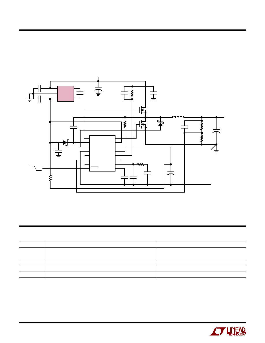
3.3V to 1.9V, 6A Power Supply
LTC1517-5
LTC1430CS
G1
PV
CC1
PGND
GND
SENSE
≠
FB
SENSE
+
SHDN
G2
PV
CC2
V
CC
I
FB
I
MAX
FREQSET
COMP
SS
1
2
3
4
5
6
7
8
16
15
14
13
12
11
10
9
C3
0.22
Ķ
F
5
1
2
3
4
C6 TO C9*
330
Ķ
F
6.3V
◊
4
C15
10
Ķ
F
10V
C13
390pF
C14
0.012
Ķ
F
C12
0.1
Ķ
F
C16
0.018
Ķ
F
V
OUT
1.9V
6A
C4
0.1
Ķ
F
5V
C5
1
Ķ
F
D1
BAT54
D2
MBRS120
R5
4.99K
1%
R6
10K
1%
L1
2.4
Ķ
H, 8A
SUMIDA
CDRH127-2R4
C11
1
Ķ
F
Q1
Si4410
Q2
Si4410
R2
24k
R4
5.2k
C10
0.1
Ķ
F
C1
Y5V CERAMIC
3.3
Ķ
F
V
IN
3.3V
C2
Y5V CERAMIC
10
Ķ
F
+
C17 TO C21 *
330
Ķ
F
6.3V
◊
5
*AVX TPS TANTALUM
1517 TA03
+
R1
100
R3
1k
ON OFF
+
TYPICAL APPLICATIO
N
U
PART NUMBER
DESCRIPTION
COMMENTS
LTC1514-X
Step-Up/Step-Down Switched-Capacitor DC/DC Converter with
3.3V or 5V Output Up to 50mA
Low Battery Comparator
LTC1515 Series
Step-Up/Step-Down Switched-Capacitor DC/DC Converter with Reset
Fixed or Adjustable Output Up to 50mA
LTC1516
Micropower Regulated 5V Charge Pump DC/DC Converter
20mA for V
IN
2V, 50mA for V
IN
3V
LTC1522
Micropower Regulated 5V Charge Pump DC/DC Converter
Same as LTC1517-5 with Shutdown, Available in MSOP
RELATED PARTS