 | –≠–ª–µ–∫—Ç—Ä–æ–Ω–Ω—ã–π –∫–æ–º–ø–æ–Ω–µ–Ω—Ç: LTC1540 | –°–∫–∞—á–∞—Ç—å:  PDF PDF  ZIP ZIP |
1
LTC1540
Nanopower Comparator
with Reference
V
+
R1
4.32M
1%
R2
3M
1%
3.3V
V
≠
2
1
7
8
GND
OUT
LTC1540
1540 ∑ TA01
IN
+
IN
≠
HYST
REF
3
4
5
6
≠
+
TEMPERATURE (
∞
C)
≠40
0.50
0.45
0.40
0.35
0.30
0.25
0.20
0.15
20
60
1540 ∑ TA02
≠20
0
40
80
100
SUPPLY CURRENT (
µ
A)
V
+
= 5V
V
≠
= GND = 0V
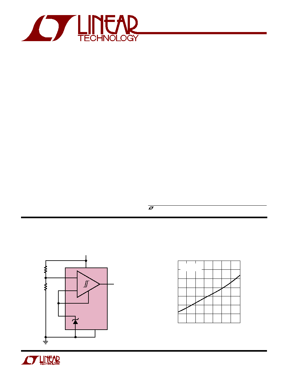
The LTC
Æ
1540 is an ultralow power, single comparator
with built-in reference. The comparator's features
include less than 0.6
µ
A supply current over the commer-
cial temperature range, a 1.182V
±
2% reference, pro-
grammable hysteresis and TTL/CMOS outputs that sink
and source current. The reference output can drive a
bypass capacitor of up to 0.01
µ
F without oscillation.
The comparator operates from a single 2V to 11V supply
or a dual
±
1V to
±
5.5V supply. Comparator hysteresis is
easily programmed by using two resistors and the HYST
pin. Each comparator's input operates from the negative
supply to within 1.3V of the positive supply. The compara-
tor output stage can continuously source up to 40mA. By
eliminating the cross-conducting current that normally
occur when the comparator changes logic states, power
supply glitches are eliminated.
The LTC1540 is available in the 8-pin MSOP and SO
packages.
FEATURES
DESCRIPTIO
N
U
TYPICAL APPLICATIO
N
U
Nanopower 2.9V V
CC
Threshold Detector
LTC1540 Supply Current vs Temperature
s
Ultralow Quiescent Current: 0.3
µ
A Typ
s
Reference Output Drives 0.01
µ
F Capacitor
s
Adjustable Hysteresis
s
Wide Supply Range: 2V to 11V
s
Input Voltage Range Includes the Negative Supply
s
Reference Output Sources Up to 1mA
s
TTL/CMOS Compatible Outputs
s
60
µ
s Propagation Delay with 10mV Overdrive
s
No Crowbar Current
s
40mA Continuous Source Current
s
Pin Compatible with LTC1440, MAX921, MAX931
, LTC and LT are registered trademarks of Linear Technology Corporation.
s
Battery-Powered System Monitoring
s
Threshold Detectors
s
Window Comparators
s
Oscillator Circuits
APPLICATIO
N
S
U
2
LTC1540
Voltage
V
+
to V
≠
, V
+
to GND, GND to V
≠
...........12V to ≠ 0.3V
IN
+
, IN
≠
, HYST ................. (V
+
+ 0.3V) to (V
≠
≠ 0.3V)
REF ................................... (V
+
+ 0.3V) to (V
≠
≠ 0.3V)
OUT ............................... (V
+
+ 0.3V) to (GND ≠ 0.3V)
Current
IN
+
, IN
≠
, HYST ................................................. 20mA
REF ................................................................... 20mA
OUT .................................................................. 50mA
ABSOLUTE
M
AXI
M
U
M
RATINGS
W
W
W
U
OUT Short-Circuit Duration (V
+
5.5V) ...... Continuous
Power Dissipation ............................................. 500mW
Operating Temperature Range
LTC1540C............................................... 0
∞
C to 70
∞
C
LTC1540I ............................................ ≠ 40
∞
C to 85
∞
C
Storage Temperature Range ................ ≠ 65
∞
C to 150
∞
C
Lead Temperature (Soldering, 10 sec).................. 300
∞
C
PACKAGE/ORDER I
N
FOR
M
ATIO
N
W
U
U
LTC1540CMS8
MS8 PART MARKING
Consult factory for Military grade parts.
V
+
= 5V, V
≠
= GND = 0V, T
A
= 25
∞
C unless otherwise noted.
ELECTRICAL CHARACTERISTICS
T
JMAX
= 125
∞
C,
JA
= 175
∞
C/ W
1
2
3
4
8
7
6
5
TOP VIEW
OUT
V
+
REF
HYST
GND
V
≠
IN
+
IN
≠
S8 PACKAGE
8-LEAD PLASTIC SO
1
2
3
4
GND
V
≠
IN
+
IN
≠
8
7
6
5
OUT
V
+
REF
HYST
TOP VIEW
MS8 PACKAGE
8-LEAD PLASTIC MSOP
T
JMAX
= 125
∞
C,
JA
= 250
∞
C/ W
ORDER PART
NUMBER
S8 PART MARKING
ORDER PART
NUMBER
LTCE
SYMBOL PARAMETER
CONDITIONS
MIN
TYP
MAX
UNITS
Power Supply
V
+
Supply Voltage Range
q
2.0
11.0
V
I
CC
Supply Current
IN
+
= IN
≠
= 80mV, HYST = REF, C-Grade
q
0.3
0.68
µ
A
IN
+
= IN
≠
= 80mV, HYST = REF, I-Grade
q
0.71
µ
A
Comparator
V
OS
Comparator Input Offset Voltage
V
CM
= 2.5V
±
12
mV
q
±
15
mV
LTC1540CMS8
q
±
16
mV
I
IN
Input Leakage Current (IN
+
, IN
≠
)
V
IN
+
= V
IN
≠
= 2.5V
q
±
0.01
±
1.0
nA
Input Leakage Current (HYST)
q
±
0.02
±
1.0
nA
V
CM
Comparator Input Common Mode Range
q
V
≠
V
+
≠ 1.3V
V
CMRR
Common Mode Rejection Ratio
V
≠
to V
+
≠ 1.3V
0.1
1
mV/V
PSRR
Power Supply Rejection Ratio
V
+
= 2V to 11V
0.1
1
mV/V
V
HYST
Hysteresis Input Voltage Range
q
REF ≠ 50mV
REF
V
t
PD
Propagation Delay
C
OUT
= 100pF
Overdrive = 10mV
60
µ
s
Overdrive = 100mV
50
µ
s
V
OH
Output High Voltage
I
O
= ≠ 13mA
q
V
+
≠ 0.4V
V
V
OL
Output Low Voltage
I
O
= 1.8mA
q
GND + 0.4V
V
LTC1540CS8
LTC1540IS8
1540
1540I
3
LTC1540
SYMBOL PARAMETER
CONDITIONS
MIN
TYP
MAX
UNITS
Reference
V
REF
Reference Voltage
(SO-8) No Load
Commercial Temp Range
q
1.158
1.182
1.206
V
Industrial Temp Range
q
1.152
1.182
1.212
V
LTC1540CMS8
q
1.156
1.182
1.208
V
V
REF
Load Regulation
0
I
SOURCE
1mA
q
0.5
2.5
mV
0
I
SINK
10
µ
A
0.5
1.5
mV
q
5
mV
V
+
= 5V, V
≠
= GND = 0V, T
A
= 25
∞
C unless otherwise noted.
ELECTRICAL CHARACTERISTICS
V
+
= 3V, V
≠
= GND = 0V, T
A
= 25
∞
C unless otherwise noted.
The
q
denotes specifications which apply over the full operating
temperature range.
Note 1: MS8 package devices are designed for and intended to meet
commercial temperature range specifications but are not tested at 0
∞
C.
SYMBOL PARAMETER
CONDITIONS
MIN
TYP
MAX
UNITS
Power Supply
V
+
Supply Voltage Range
q
2
11
V
I
CC
Supply Current
IN
+
= IN
≠
= 80mV, HYST = REF, C-Grade
q
0.28
0.61
µ
A
IN
+
= IN
≠
= 80mV, HYST = REF, I-Grade
q
0.64
µ
A
Comparator
V
OS
Comparator Input Offset Voltage
V
CM
= 2.5V
±
12
mV
q
±
15
mV
LTC1540CMS8
q
±
16
mV
I
IN
Input Leakage Current (IN
+
, IN
≠
)
V
IN
+
= V
IN
≠
= 1.5V
q
±
0.01
±
1
nA
Input Leakage Current (HYST)
q
±
0.02
±
1
nA
V
CM
Comparator Input Common Mode Range
q
V
≠
V
+
≠ 1.3V
V
CMRR
Common Mode Rejection Ratio
V
≠
to V
+
≠ 1.3V
0.1
1
mV/V
PSRR
Power Supply Rejection Ratio
V
+
= 2V to 11V
0.1
1
mV/V
V
HYST
Hysteresis Input Voltage Range
q
REF ≠ 50mV
REF
V
t
PD
Propagation Delay
C
OUT
= 100pF
Overdrive = 10mV
70
µ
s
Overdrive = 100mV
60
µ
s
V
OH
Output High Voltage
I
O
= ≠ 8mA
q
V
+
≠ 0.4V
V
V
OL
Output Low Voltage
I
O
= 0.8mA
q
GND + 0.4V
V
Reference
V
REF
Reference Voltage
(SO-8) No Load
Commercial Temp Range
q
1.158
1.182
1.206
V
Industrial Temp Range
q
1.152
1.182
1.212
V
LTC1540CMS8
q
1.156
1.182
1.208
V
V
REF
Load Regulation
0
I
SOURCE
1mA
q
0.75
3.5
mV
0
I
SINK
10
µ
A
0.5
1.5
mV
q
5
mV
4
LTC1540
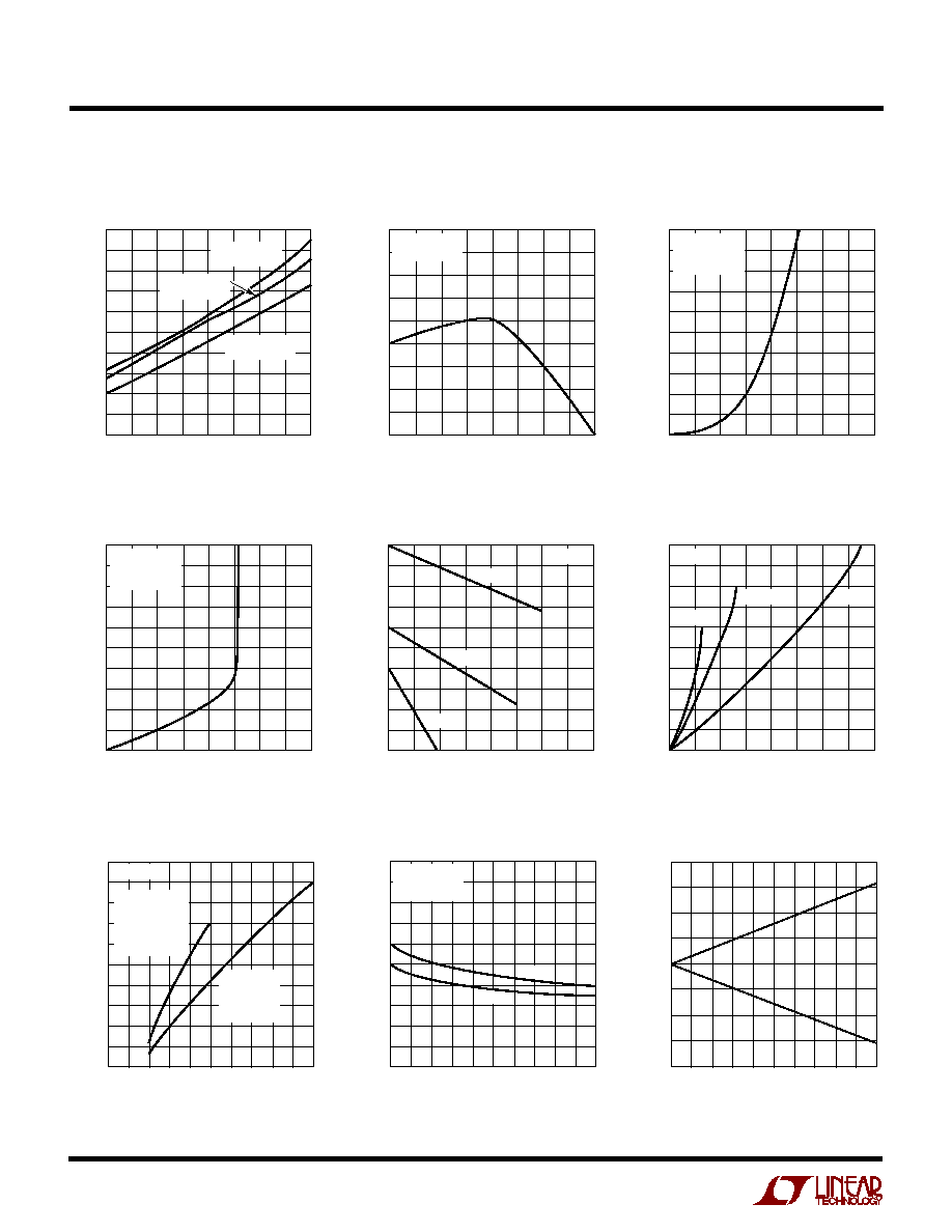
TYPICAL PERFOR
M
A
N
CE CHARACTERISTICS
U
W
TEMPERATURE (
∞
C)
≠ 60
0
SUPPLY CURRENT (
µ
A)
0.2
0.5
≠20
20
40
1540 G01
0.1
0.4
0.3
≠ 40
0
60
80
100
V
+
= 5V
V
≠
= GND = 0V
V
+
= 2V
V
≠
= GND = 0V
V
+
= 3V
V
≠
= GND = 0V
Supply Current vs Temperature
Reference Voltage
Load Regulation (Source)
OUTPUT SOURCE CURRENT (mA)
0
0
V
REF
(mV)
2
5
1
2
1540 G04
1
4
3
3
4
V
+
= 5V
V
≠
= GND = 0V
T
A
= 25
∞
C
Comparator Short-Circuit Current
vs Supply Voltage
SUPPLY VOLTAGE (V)
0
CURRENT (mA)
120
160
200
8
1540 G07
80
40
100
140
180
60
20
0
2
4
6
1
9
3
5
7
10
T
A
= 25
∞
C
OUTPUT
CONNECTED TO
V
≠
= GND = 0V;
SOURCE
CURRENT
OUTPUT
CONNECTED
TO V
+
; SINK
CURRENT
V
REF
≠ V
HYST
(mV)
0
DIFFERENTIAL INPUT VOLTAGE (V)
80
60
40
20
0
≠ 20
≠ 40
≠ 60
≠ 80
40
1540 G09
10
20
30
50
Hysteresis Control
Comparator Output Voltage (Low)
vs Load Current
LOAD CURRENT (mA)
0
0
OUTPUT VOLTAGE (V)
1.0
2.5
20
40
1540 G06
0.5
2.0
1.5
60
80
10
30
50
70
T
A
= 25
∞
C
V
+
= 5V
V
+
= 3V
V
+
= 2V
Reference Voltage
Load Regulation (Sink)
OUTPUT SINK CURRENT (
µ
A)
0
0
V
REF
(mV)
1
3
4
5
10
7
10
20
25
1540 G03
2
8
9
6
5
15
30
35
40
V
+
= 5V
V
≠
= GND = 0V
T
A
= 25
∞
C
TEMPERATURE (
∞
C)
≠ 60
REFERENCE VOLTAGE (V)
1.182
1.184
1.186
80
100
1540 G02
1.180
1.178
1.172
≠ 40
0
20
≠ 20
40
60
1.174
1.176
1.190
1.188
V
+
= 5V
V
≠
= GND = 0V
Reference Voltage vs Temperature
Comparator Output Voltage (High)
vs Load Current
LOAD CURRENT (mA)
0
0
OUTPUT VOLTAGE (V)
2
5
20
40
1540 G05
1
4
3
60
80
10
30
50
70
T
A
= 25
∞
C
V
+
= 5V
V
+
= 3V
V
+
= 2V
Comparator Response Time
vs Input Overdrive
INPUT VOLTAGE (mV)
TIME (
µ
s)
60
70
80
80
1540 G08
50
40
55
65
75
45
35
30
20
40
60
10
90
30
50
70
100 110
T
A
= 25
∞
C
V
+
= 5V
V
≠
= GND = 0V
t
PLH
t
PHL
5
LTC1540
PI
N
FU
N
CTIO
N
S
U
U
U
V
+
(Pin 7): Positive Supply operating voltage is from 2V
to 11V.
OUT (Pin 8): Comparator CMOS Output. Swings from
GND to V
+
. Output can source up to 40mA and sink 5mA.
GND (Pin 1): Ground. Connect to V
≠
for single supply
operation.
V
≠
(Pin 2): Negative Supply. Potential should be more
negative than GND. Connect to ground for single supply
operation.
IN
+
(Pin 3): Noninverting Comparator Input. Input com-
mon mode range from V
≠
to V
+
≠ 1.3V. Input current
typically 10pA at 25
∞
C.
IN
≠
(Pin 4): Inverting Comparator Input. Input common
mode range from V
≠
to V
+
≠ 1.3V. Input current typically
10pA at 25
∞
C.
HYST (Pin 5): Hysteresis Input. Connect to REF if not
used. Input voltage range is from V
REF
to V
REF
≠ 50mV.
REF (Pin 6): Reference Output. 1.182V with respect
to V
≠
. Can source up to 1mA and sink 10
µ
A at 25
∞
C. Drive
0.01
µ
F bypass capacitor without oscillation.
1540 ∑ PD
1
2
3
4
8
7
6
5
IN
+
IN
≠
HYST
REF
V
+
OUT
≠
+
V
≠
GND
LTC1540
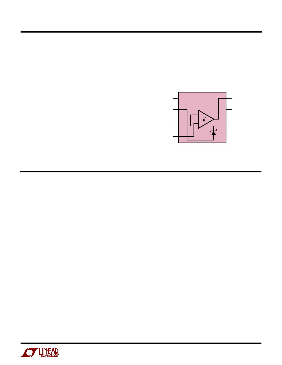
The LTC1540 is a nanopower comparator with a built-in
1.182V reference. Features include programmable hyster-
esis, wide supply voltage range (2V to 11V) and the ability
of the reference to drive up to a 0.01
µ
F capacitor without
oscillation. The comparator's CMOS outputs can source
up to 40mA while supply current glitches that normally
occur when switching logic states, have been eliminated.
Power Supplies
The comparator operates from a single 2V to 11V supply.
The LTC1540 includes a separate ground for the compara-
tor output stage, allowing a split supply ranging from
±
1V
to
±
5.5V. Connecting V
≠
to GND will allow single supply
operation. If the comparator output is required to source
more than 1mA, or the supply source impedance is high,
V
+
should be bypassed with a 0.1
µ
F capacitor.
Comparator Inputs
The comparator inputs can swing from the negative supply,
V
≠
, to within 1.3V (max) of the positive supply V
+
. The
inputs can be forced 300mV below V
≠
or above V
+
without
damage and the typical input leakage current is only
±
10pA.
APPLICATIO
N
S I
N
FOR
M
ATIO
N
W
U
U
U
Comparator Output
The comparator output swings between GND and V
+
to
assure TTL compatibility with a split supply. The output is
capable of sourcing up to 40mA and sinking up to 5mA
while still maintaining nanoampere quiescent currents.
The output stage does not generate crowbar switching
currents during transitions which helps minimize parasitic
feedback through the supply pins.
Voltage Reference
The internal bandgap reference has a voltage of 1.182V
referenced to V
≠
. The reference accuracy is
±
2.0% from
0
∞
C to 70
∞
C. It can source up to 1mA and sink up to 10
µ
A
with a 5V supply. The reference can drive a bypass
capacitor of up to 0.01
µ
F without oscillation and by
inserting a series resistor, capacitance values up to 10
µ
F
can be used (Figure 1).
Figure 2 shows the resistor value required for different
capacitor values to achieve critical damping. Bypassing
the reference can help prevent false tripping of the com-
parators by preventing glitches on V
+
or reference load
transients from disturbing the reference output voltage.