 | –≠–Ľ–Ķ–ļ—ā—Ä–ĺ–Ĺ–Ĺ—č–Ļ –ļ–ĺ–ľ–Ņ–ĺ–Ĺ–Ķ–Ĺ—ā: LTC1590 | –°–ļ–į—á–į—ā—Ć:  PDF PDF  ZIP ZIP |

1
LTC1590
Dual Serial 12-Bit
Multiplying DAC
Daisy-Chained Control Outputs
The LTC
ģ
1590 is a dual, serial input 12-bit multiplying
digital-to-analog converter (DAC). It includes two current
output multiplying CMOS DACs and an easy SPI compat-
ible serial interface with daisy-chain output. An asynchro-
nous CLR pin sets both DACs to zero scale.
Excellent accuracy, stability and versatility are combined
with the smallest package available for a dual 12-bit
multiplying DAC.
Parts are available in 16-pin PDIP and narrow SO pack-
ages and are specified over the commercial and industrial
temperature ranges.
DESCRIPTIO
N
U
FEATURES
s
DNL and INL Over Temperature:
Ī
0.5LSB Max
s
Gain Error:
Ī
1LSB Max
s
Low Supply Current: 10
Ķ
A Max
s
4-Quadrant Multiplication
s
Power-On Reset
s
Asynchronous Clear Input
s
Daisy-Chain 3-Wire Serial Interface
s
16-Pin Narrow SO and PDIP Packages
APPLICATIO
N
S
U
s
Process Control and Industrial Automation
s
Software Controlled Gain Adjustment
s
Digitally Controlled Filter and Power Supplies
s
Automatic Test Equipment
, LTC and LT are registered trademarks of Linear Technology Corporation.
TYPICAL APPLICATIO
N
U
Integral Nonlinearity Over
Temperature DAC A
DIGITAL INPUT CODE
0
INL (LSB)
1024
2048
3072
4095
LTC1590 ∑ TA02
1.0
0.5
0
≠0.5
≠1.0
512
1536
2560
3584
THREE
SUPERIMPOSED
CURVES
T
A
= ≠40
į
C,
25
į
C, 85
į
C
DIGITAL INPUT CODE
0
INL (LSB)
1024
2048
3072
4095
LTC1590 ∑ TA03
1.0
0.5
0
≠0.5
≠1.0
512
1536
2560
3584
THREE
SUPERIMPOSED
CURVES
T
A
= ≠40
į
C,
25
į
C, 85
į
C
Integral Nonlinearity Over
Temperature DAC B
13
16
9
1 2
12
10
LTC1590 ∑ TA01
14
11
3
6
5
4
8
V
OUT B
Ī
10V
V
OUT A
Ī
10V
5V
V
IN A
Ī
10V
V
IN B
Ī
10V
15
5V
7
33pF
33pF
LT
ģ
1112
15V
≠15V
DAC B
V
CC
V
REF B
R
FB B
V
REF A
R
FB A
DAC A
24-BIT
SHIFT
REG
AND
LATCH
D
IN
D
OUT
CLK
CS/LD
CLR
DGND
AGND
LTC1590
OUT1 B
OUT2 B
OUT1 A
OUT2 A
Ķ
P
+
≠
+
≠
Dual 12-Bit 2-Quadrant Multiplying DAC
2
LTC1590
ABSOLUTE
M
AXI
M
U
M
RATINGS
W
W
W
U
W
U
U
PACKAGE/ORDER I FOR ATIO
Consult factory for Military grade parts.
ELECTRICAL CHARACTERISTICS
V
CC
to AGND ............................................... ≠ 0.5V to 7V
V
CC
to DGND .............................................. ≠ 0.5V to 7V
AGND to DGND ............................................. V
CC
+ 0.5V
DGND to AGND .............................................. V
CC
+ 0.5V
V
REF
to AGND ........................................................
Ī
25V
R
FB
to AGND ..........................................................
Ī
25V
Digital Inputs to DGND ................... ≠ 0.5V to V
CC
+ 0.5V
V
OUT1
, V
OUT2
to AGND .................... ≠ 0.5V to V
CC
+ 0.5V
Maximum Junction Temperature .......................... 150
į
C
Operating Temperature Range
LTC1590C ................................................ 0
į
C to 70
į
C
LTC1590I ............................................ ≠ 40
į
C to 85
į
C
Storage Temperature Range ................ ≠ 65
į
C to 150
į
C
Lead Temperature (Soldering, 10 sec) ................. 300
į
C
LTC1590CN
LTC1590CS
LTC1590IN
LTC1590IS
ORDER PART
NUMBER
V
CC
= 4.5V to 5.5V, V
REF
= 10V, V
OUT1
= V
OUT2
= AGND = DGND = 0V, T
A
= T
MIN
to T
MAX
, unless otherwise noted.
T
JMAX
= 150
į
C,
JA
= 100
į
C/W (N)
T
JMAX
= 150
į
C,
JA
= 150
į
C/W (S)
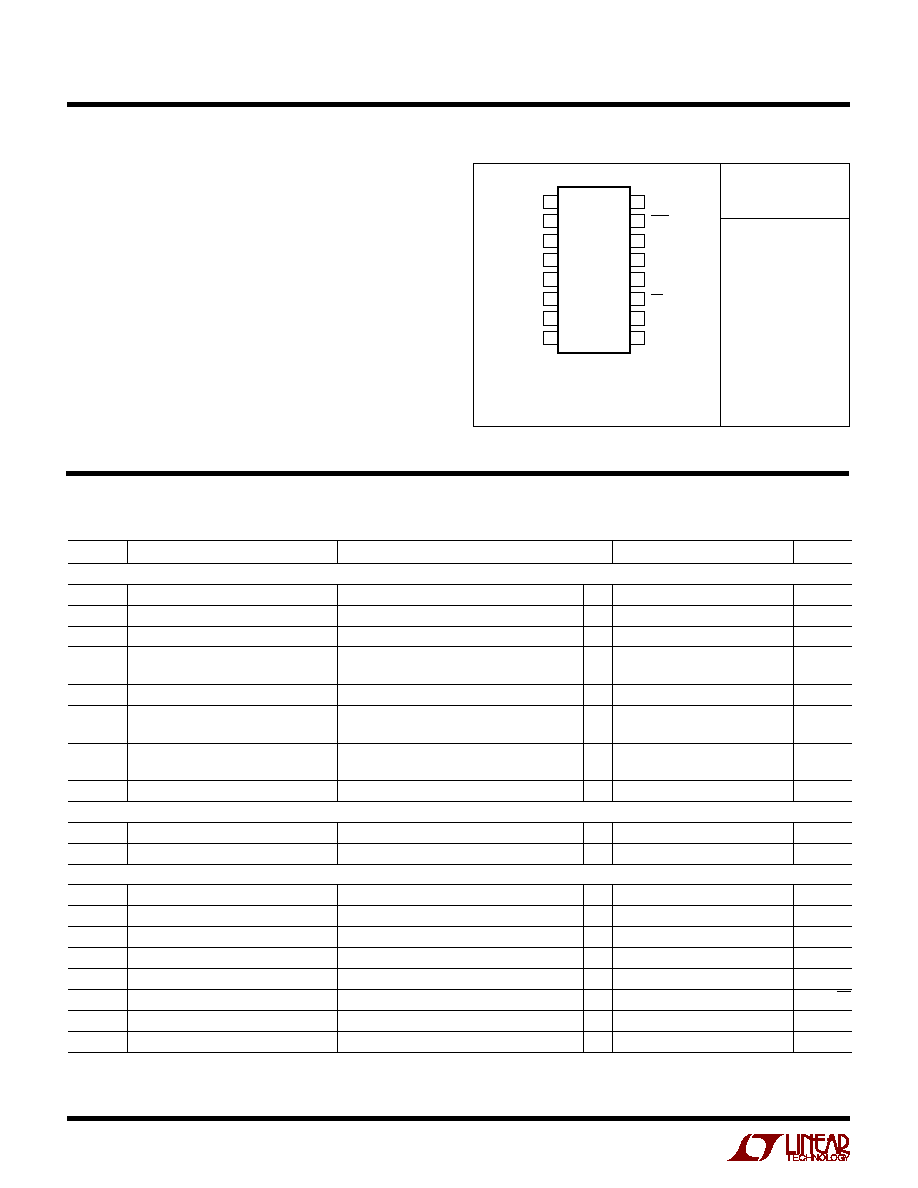
TOP VIEW
S PACKAGE
16-LEAD PLASTIC SO
N PACKAGE
16-LEAD PDIP
1
2
3
4
5
6
7
8
16
15
14
13
12
11
10
9
V
REF B
R
FB B
OUT1 B
OUT2 B
OUT2 A
OUT1 A
AGND
R
FB A
V
CC
CLR
CLK
D
IN
D
OUT
CS/LD
DGND
V
REF A
SYMBOL
PARAMETER
CONDITIONS
MIN
TYP
MAX
UNITS
Accuracy
Resolution
q
12
Bits
INL
Integral Nonlinearity
(Note 1)
q
Ī
0.5
LSB
DNL
Differential Nonlinearity
Guaranteed Monotonic, T
MIN
to T
MAX
q
Ī
0.5
LSB
GE
Gain Error
(Note 2), T
A
= 25
į
C
Ī
1
LSB
T
MIN
to T
MAX
q
Ī
2
LSB
Gain Temperature Coefficient
(Note 3)
Gain/
Temperature
q
1
5
ppm/
į
C
I
LEAKAGE
OUT1 A, OUT1 B Leakage Current
(Note 4), T
A
= 25
į
C
Ī
5
nA
T
MIN
to T
MAX
q
Ī
25
nA
Zero-Scale Error
T
A
= 25
į
C
Ī
0.03
LSB
T
MIN
to T
MAX
q
Ī
0.15
LSB
PSRR
Power Supply Rejection
V
CC
= 5V
Ī
10%
q
Ī
0.0001
Ī
0.002
%/%
Reference Input
R
REF
V
REF
Input Resistance
q
8
11
15
k
V
REFA
, V
REFB
Input Resistance Match
q
3
%
AC Performance (Note 3)
Digital-to-Analog Glitch Impulse
(Notes 5, 6)
1
nV-s
Multiplying Feedthrough Error
(Note 11)
≠ 89
≠ 80
dB
Output Current Settling Time
(Note 5) To 0.01% for Full-Scale Change
0.3
0.8
Ķ
s
Channel-to-Channel Isolation
(Note 7)
≠ 90
dB
Digital Crosstalk
(Notes 5, 8)
1
nV-s
Output Noise Voltage Density
(Note 9)
13
nV/
Hz
THD
Total Harmonic Distortion
(Note 10)
≠ 108
≠ 92
dB
Multiplying Bandwidth
(Note 12)
1
MHz
3
LTC1590
V
CC
= 4.5V to 5.5V, V
REF
= 10V, V
OUT1
= V
OUT2
= AGND = DGND = 0V, T
A
= T
MIN
to T
MAX
, unless otherwise noted.
ELECTRICAL CHARACTERISTICS
SYMBOL
PARAMETER
CONDITIONS
MIN
TYP
MAX
UNITS
Analog Outputs
C
OUT
Output Capacitance (Note 3)
DAC Register Loaded to All 1s
q
60
90
pF
DAC Register Loaded to All 0s
q
30
60
pF
Digital Input
V
IH
Digital Input High Voltage
q
2.4
V
V
IL
Digital Input Low Voltage
q
0.8
V
I
IN
Digital Input Current
q
0.001
Ī
1
Ķ
A
C
IN
Digital Input Capacitance
(Note 3) V
IN
= 0V
q
8
pF
Digital Output
V
OH
Digital Output High Voltage
I
OH
= 200
Ķ
A
q
4
V
V
OL
Digital Output Low Voltage
I
OH
= 1.6mA
q
0.4
V
Timing Characteristics
t
1
D
IN
to CLK Setup Time
q
50
ns
t
2
D
IN
to CLK Setup Hold Time
q
0
ns
t
3
CLK High Time
q
40
ns
t
4
CLK Low Time
q
40
ns
t
5
CS/LD High Time
q
50
ns
t
6
LSB CLK to CS/LD
q
40
ns
t
7
CS/LD Low to CLK High
q
20
ns
t
8
CLK Low to CS/LD Low
q
20
ns
t
9
CLK to D
OUT
Delay
q
10
160
ns
Power Supply
V
CC
Operating Supply Range
q
4.5
5
5.5
V
I
CC
Supply Current
Digital Inputs = 0V or V
CC
q
10
Ķ
A
Note 8: Glitch on DAC A or DAC B output when the other DAC makes a
full-scale transition.
Note 9: 10Hz to 100kHz. Calculation from e
n
=
4KTRB where:
K = Boltzmann constant (J/K
į
); R = resistance (
); T = resistor temperature
(
į
K); B = bandwidth (Hz).
Note10: V
REF
= 6V
RMS
at 1kHz. DAC register loaded with all 1s, using
LT
ģ
1124 op amp.
Note 11: V
REF
=
Ī
10V, 10kHz sine wave, DAC register loaded with all 0s,
using LT1358 op amp.
Note 12: ≠3dB bandwidth using LT1358 op amp.
The
q
denotes specifications which apply over the full operating
temperature range.
Note 1:
Ī
0.5LSB =
Ī
0.012% of full scale.
Note 2: Using internal feedback resistor.
Note 3: Guaranteed by design, not subject to test.
Note 4: I
OUT1
with DAC register loaded with all 0s.
Note 5: OUT1 load = 100
in parallel with 13pF.
Note 6: V
REF
= 0V. DAC register contents changed from all 0s to all 1s or
all 1s to all 0s.
Note 7: DAC A output with V
REF A
= 0V and V
REF B
= 10kHz 20V
P-P
, or
DAC B output with V
REF B
= 0V, V
REF A
= 10kHz 20V
P-P
. Both DAC registers
loaded with all 1s.
4
LTC1590
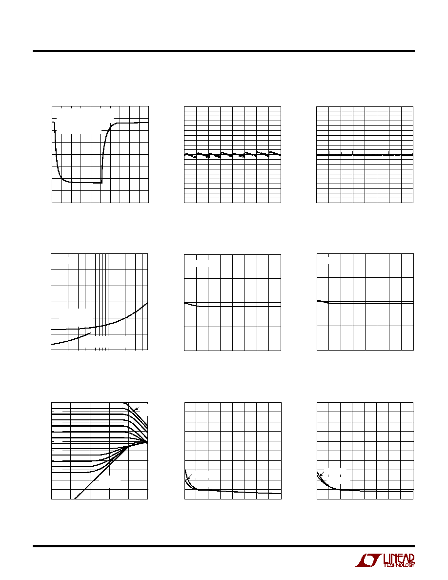
TYPICAL PERFOR
M
A
N
CE CHARACTERISTICS
U
W
Differential Nonlinearity (DNL)
DIGITAL INPUT CODE
0
DIFFERENTIAL NONLINEARITY (LSB)
1024
2048
3072
4095
1590 G03
1.0
0.5
0
≠0.5
≠1.0
512
1536
2560
3584
Differential Nonlinearity vs
Reference Voltage
SUPPLY VOLTAGE (V)
DIFFERENTIAL NONLINEARITY (LSB)
1.0
0.9
0.8
0.7
0.6
0.5
0.4
0.3
0.2
0.1
0
1590 G09
2
3
4
5
6
7
8
9
10
V
REF
= 10V
V
REF
= 2V
Integral Nonlinearity (INL)
Integral Nonlinearity vs
Reference Voltage
REFERENCE VOLTAGE (V)
2
INTEGRAL NONLINEARITY (LSB)
10
1590 G05
4
6
8
0.20
0.15
0.10
0.05
0
3
5
7
9
V
DD
= 5V
Differential Nonlinearity vs
Supply Voltage
DIGITAL INPUT CODE
0
INTEGRAL NONLINEARITY (LSB)
1024
2048
3072
4095
1590 G02
1.0
0.5
0
≠0.5
≠1.0
512
1536
2560
3584
FREQUENCY (Hz)
100
ATTENUATION (dB)
0
10
20
30
40
50
60
70
80
90
100
1M
1590 G07
1k
10k
100k
10M
D11
D10
D9
D8
D7
D6
D5
D4
D3
D2
D1
D0
ALL BITS
OFF
ALL BITS
ON
Multiplying Mode Frequency
Response vs Digital Code
SUPPLY VOLTAGE (V)
INTEGRAL NONLINEARITY (LSB)
1.0
0.9
0.8
0.7
0.6
0.5
0.4
0.3
0.2
0.1
0
1590 G08
2
3
4
5
6
7
8
9
10
V
REF
= 10V
V
REF
= 2V
Integral Nonlinearity vs
Supply Voltage
REFERENCE VOLTAGE (V)
DIFFERENTIAL NONLINEARITY (LSB)
1590 G06
2
3
4
5
6
7
8
9
10
V
DD
= 5V
0.20
0.15
0.10
0.05
0
FREQUENCY (kHz)
1
SIGNAL-TO-(NOISE + DISTORTION) (dB)
≠50
≠60
≠70
≠80
≠90
≠100
≠110
10
50
1590 G10
V
DD
= 5V
USING AN
LT1363 WITH
500kHz FILTER
USING AN LT1007
WITH 22kHz FILTER
Multiplying Mode Signal-to-
(Noise + Distortion) vs Frequency
TIME (500ns/DIV)
OUTPUT VOLTAGE (1V/DIV)
1590 G12
V
DD
= 5V
0V TO 5V OUTPUT RANGE
LT1363 OP AMP
C
FB
30pF
Full-Scale Settling Waveform
5
LTC1590
TYPICAL PERFOR
M
A
N
CE CHARACTERISTICS
U
W
enabled so the data can be clocked in. When CS/LD is
pulled high, data is loaded from the shift register into the
DAC register, updating the DAC output.
D
OUT
(Pin 12): The Serial Data Output. Data becomes valid
on the rising edge of the CLK.
D
IN
(Pin 13): The Serial Data Input. Data on the D
IN
pin is
latched into the shift register on the rising edge of the serial
clock. Data is loaded as one 24-bit word. The first 12 bits
are for DAC A, MSB-first and the second 12 bits are for
DAC B, MSB-first.
CLK (Pin 14): The Serial Interface Clock Input.
CLR (Pin 15): The Clear Pin for the DAC. Clears both DACs
to zero scale when pulled low. This pin should be tied to
V
CC
for normal operation.
V
CC
(Pin 16): The Positive Supply Input. 4.5
V
CC
5.5V. Requires a bypass capacitor to ground.
V
REF B
, V
REF A
(Pins 1, 9): Reference Inputs for DAC A/B.
Typically
Ī
10V, accepts up to
Ī
25V.
R
FB B
, R
FB A
(Pins 2, 8): Feedback Resistors for DAC A/B.
Normally tied to the output of current to voltage converter
op amp. Typically swings to
Ī
10V. Swings from 0V to
≠ V
REF
.
OUT1 B, OUT1 A (Pins 3, 6): True Current Output for DAC
A/B. Normally tied to inverting input of current to voltage
converter op amp.
OUT2 B, OUT2 A (Pins 4, 5): Complement Current Output
for DAC A/B. Normally tied to ground.
AGND (Pin 7): Analog Ground Pin. Tie to ground.
DGND (Pin 10): Digital Ground Pin. Tie to ground.
CS/LD (Pin 11): The Serial Interface Enable and Load
Control Input. When CS/LD is low the CLK signal is
PI
N
FU
N
CTIO
N
S
U
U
U
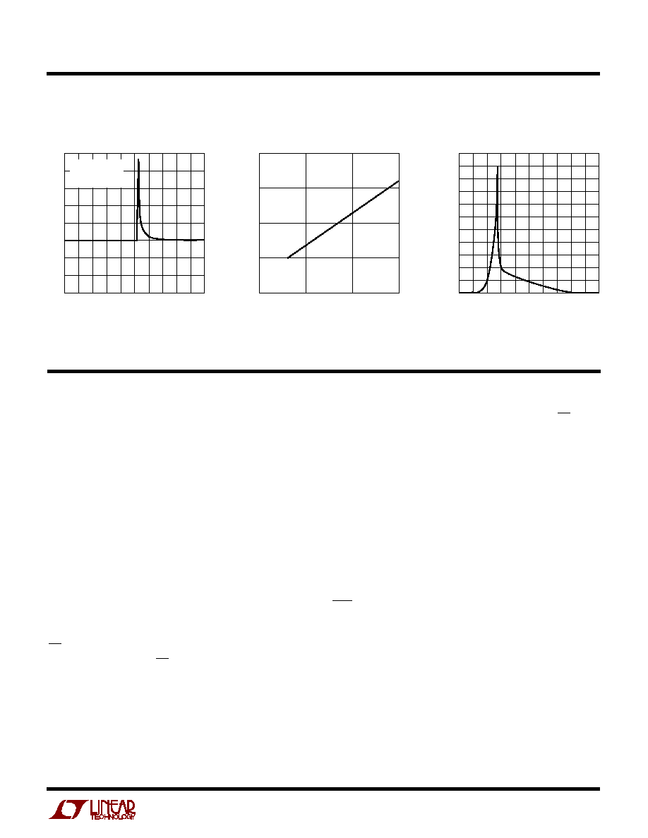
INPUT VOLTAGE (V)
0
SUPPLY CURRENT (mA)
1.0
0.5
0
4
1590 G01
1
2
3
5
Supply Current vs
Logic Input Voltage
TIME (500ns/DIV)
OUTPUT VOLTAGE (50mV/DIV)
1590 G11
V
DD
= 5V
LT1363 OP AMP
C
FB
= 30pF
SUPPLY VOLTAGE (V)
0
LOGIC THRESHOLD (V)
4
3
2
1
0
5
10
1590 G04
15
Logic Threshold vs
Supply Voltage
Midscale Glitch Impulse
6
LTC1590
W
I
D AGRA
BLOCK
D
IN
CLK
CS/LD
1
2
3
4
5
6
7
8
9
10
11
12
13
14
15
16
17
18
19
20
21
22
23
24
DAC B INPUT
DAC A INPUT
LTC1590 ∑ TD
D11
D9
D8
D7
D6
D5
D4
D3
D2
D1
D0
D10
D11
D9
D8
D7
D6
D5
D4
D3
D2
D1
D0
D10
(UPDATE DAC OUTPUT)
(ENABLE CLOCK)
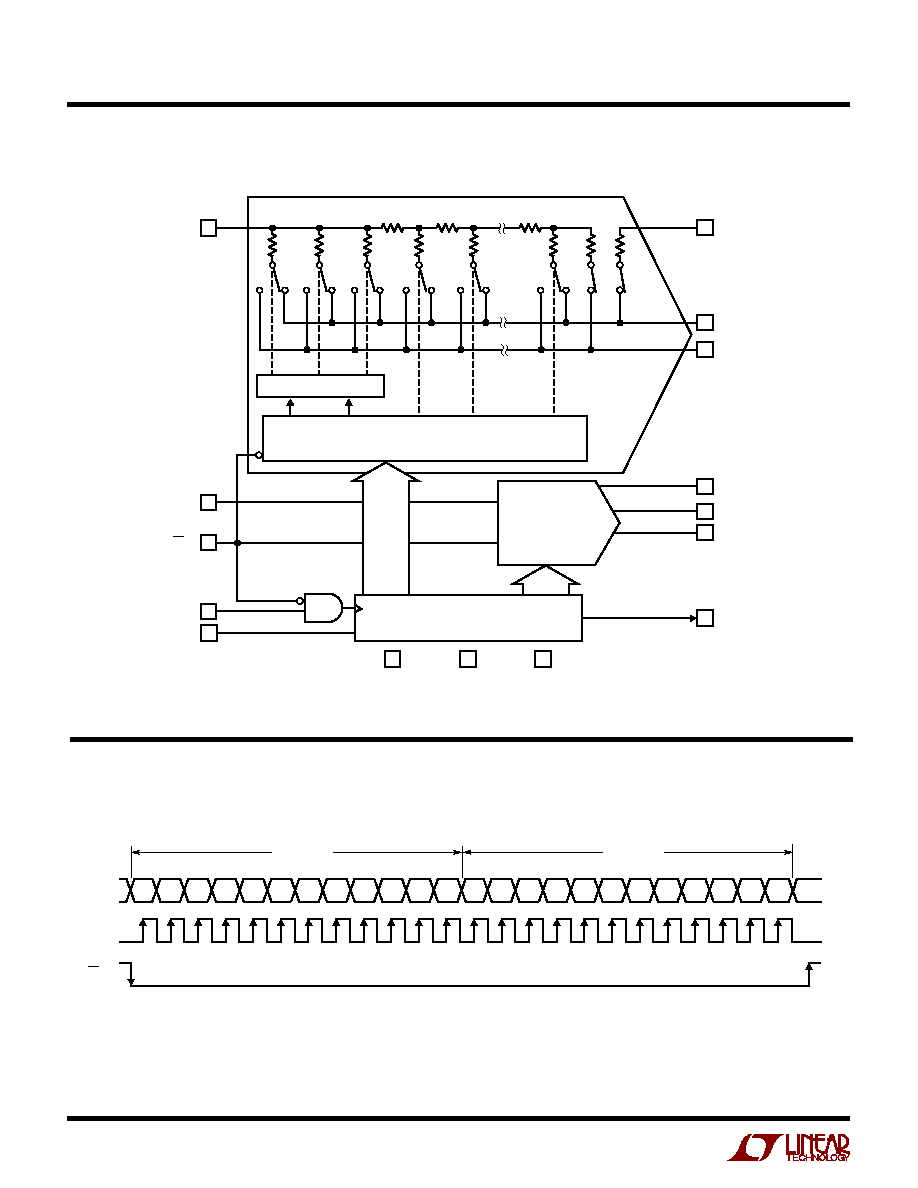
OPERATING SEQUENCE
MSB
MSB
LSB
LSB
TI
M
I
N
G DIAGRA
M
S
W
U
W
40k
10k
40k
20k
40k
20k
40k
20k
40k
40k
40k
DECODER
D11
(MSB)
D10
D9
D8
D0
(LSB)
LOAD
V
REF B
R
FB B
OUT1 B
D
OUT
12
OUT2 B
4
OUT1 A
6
OUT2 A
5
R
FB A
8
3
2
1590 ∑ BD
DAC REGISTER B
14
1
CLK
11
CS/LD
9
V
REF A
13
D
IN
DAC B
DAC A
12
12
16
10
7
V
CC
DGND
AGND
CLK
OUT
INPUT 24-BIT SHIFT REGISTER
IN
7
LTC1590
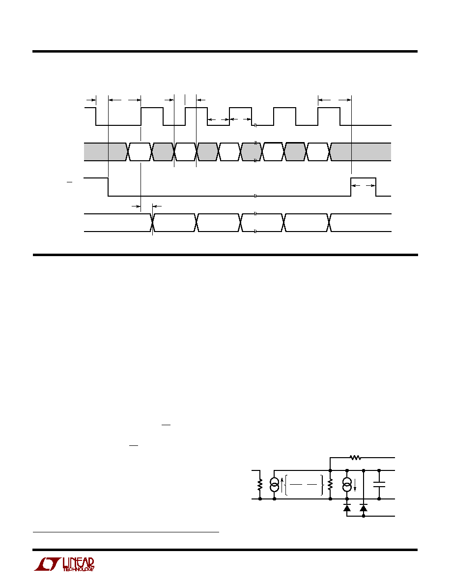
TI
M
I
N
G DIAGRA
M
S
W
U
W
D11 A
MSB
D10 A
D9 A
D1 B
t
1
t
6
D0 B
LSB
t
2
t
4
t
3
t
9
CLK
D
IN
D
OUT
CS/LD
t
5
1590 TD02
D11 A
PREVIOUS WORD
D10 A
PREVIOUS WORD
D0 B
PREVIOUS WORD
D11 A
CURRENT WORD
D9 A
PREVIOUS WORD
t
8
t
7
1
2
3
23
24
TIMING DIAGRAM
APPLICATIO
N
S I
N
FOR
M
ATIO
N
W
U
U
U
Description
The LTC1590 is a dual 12-bit multiplying DAC that has
serial inputs and current outputs. It uses precision R/2R
resistor ladder technology to provide exceptional linearity
and stability. The device operates from a single 5V supply
and provides a
Ī
10V reference input and voltage output
range when used with an external op amp.
Serial I/O
The LTC1590 has a 3-wire SPI/MICROWIRE
TM
compatible
serial port that accepts 24-bit serial words. Data is loaded
MSB first with the first 12 bits controlling DAC A and the
second 12 bits controlling DAC B. Data is shifted into the
D
IN
input on the rising edge of CLK. The CS/LD input must
be taken low before transferring data to enable the CLK
input. After transferring data, CS/LD is pulled high to load
data from the shift register to the DAC registers which
updates both DACs.
The buffered output of the 24-bit shift register is available
on the D
OUT
pin. Multiple DACs can be daisy-chained on
one 3-wire interface by connecting the D
OUT
pin to the D
IN
pin of the next DAC (see the Timing Diagrams section).
MICROWIRE is a trademark of National Semiconductor Corporation.
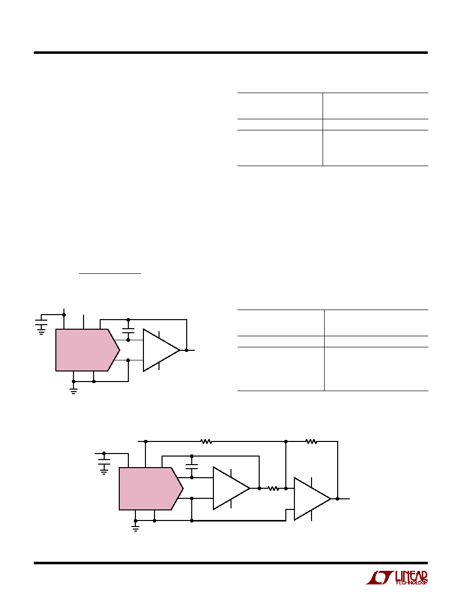
R
R
R
O
V
REF A
V
REF B
R
FB A
R
FB B
OUT1 A
OUT1 B
OUT2 A
OUT2 B
AGND
1590 F01
I
LKG
C
OUT
CODE
4096
V
REF
R
( )( )
Equivalent Circuit
Figure 1 shows an equivalent analog circuit for the LTC1590
DACs. R is the reference input, R
REF
, which is nominally
11k. The DAC output is represented by the Thevinin
equivalent current source with a value of:
(Code/4096)(V
REF
/R)
The current source I
LKG
models the junction leakage of the
DAC output switches. I
LKG
is typically less than 5nA at
85
į
C and decreases by roughly two times for every 10
į
C
reduction in temperature. C
OUT
is the output capacitance,
and it also comes from the DAC output switches and varies
from 30pF at zero scale to 60pF at full scale. R
O
is the
equivalent output resistance, which varies with digital
input code (see Op Amp Selection section).
Figure 1. Equivalent Circuit
8
LTC1590
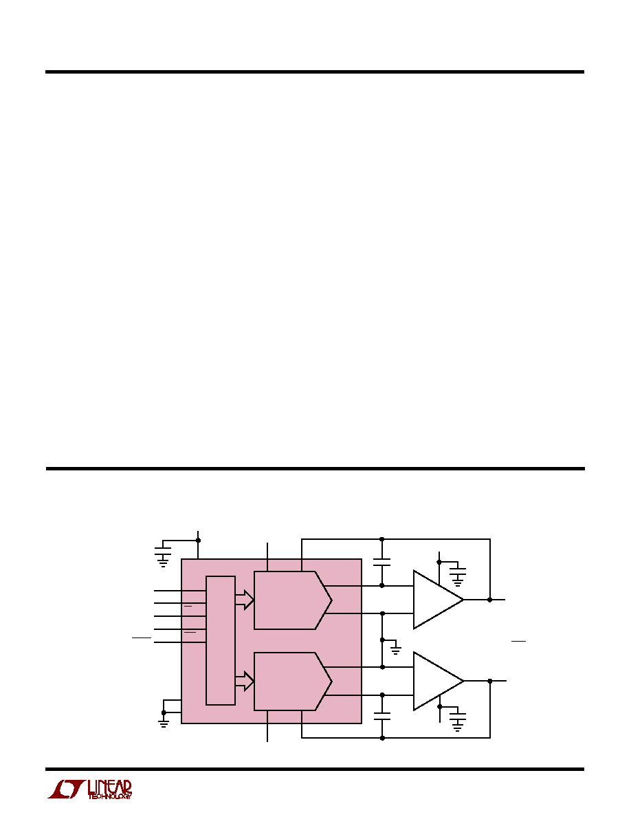
Unipolar 2-Quadrant Multiplying Mode
(V
OUT
= 0V to ≠ V
REF
)
The LTC1590 can be used with a dual op amp to provide
a dual 2-quadrant multiplying DAC as shown in Figure 2.
The unipolar DAC transfer function is shown in Table 1.
The 33pF feedback capacitor is recommended to compen-
sate for the pole caused by the internal feedback resistor
and the OUT1 output capacitance. For high speed op amps
this feedback capacitor is required for stability, and a
smaller value, 8pF to 15pF, may be desired to get the
fastest transient response and shortest settling time. A
larger feedback capacitor can be used to reduce wideband
noise, glitch impulse and distortion for lower frequency
signals. A pole is introduced in the DAC transfer function
at approximately (C
FB
)(R
FB
). For example, a 100pF feed-
back capacitor will typically give a pole at:
145
1
2 100
11
kHz
pF
k
=
( )( )
APPLICATIO
N
S I
N
FOR
M
ATIO
N
W
U
U
U
Figure 3. Bipolar Operation (4-Quadrant Multiplication)
≠15V
5V
0.1
Ķ
F
V
CC
V
REF
LTC1590
DAC A OR DAC B
R
FB
DGND
AGND
V
REF
≠10V TO 10V
OUT1
OUT2
V
OUT
≠V
REF
TO V
REF
1590 F03
15V
≠
+
1/2
LT1112
R3
20k
R1
10k
R2
20k
15V
≠15V
≠
+
1/2
LT1112
33pF
Table 1. Unipolar Binary Code Table
DIGITAL INPUT
BINARY NUMBER
ANALOG OUTPUT
IN DAC REGISTER
V
OUT
MSB LSB
1111 1111 1111
≠ V
REF
(4095/4096)
1000 0000 0000
≠ V
REF
(2048/4096) = ≠ V
REF
/2
0000 0000 0001
≠ V
REF
(1/4096)
0000 0000 0000
0V
Bipolar 4-Quadrant Multiplying Mode
(V
OUT
= ≠ V
REF
to +V
REF
)
The circuit of Figure 3 can be used to provide a dual
4-quadrant multiplying DAC. This circuit starts with the
unipolar application circuit and adds three resistors and an
op amp. These extra devices provide a gain of ≠ 2 from the
unipolar output to the bipolar output, plus an offset of
(≠1)(V
REF
) to produce the transfer function shown in Table
2. A pack of matched 20k resistors, with two resistors in
parallel forming the 10k resistor, is recommended.
Table 2. Bipolar Offset Binary Code Table
DIGITAL INPUT
BINARY NUMBER
ANALOG OUTPUT
IN DAC REGISTER
V
OUT
MSB LSB
1111 1111 1111
+V
REF
(2047/2048)
1000 0000 0001
+V
REF
(1/2048)
1000 0000 0000
0V
0111 1111 1111
≠ V
REF
(1/2048)
0000 0000 0000
≠ V
REF
(2048/2048) = ≠ V
REF
V
CC
V
REF
LTC1590
DAC A OR DAC B
R
FB
DGND
AGND
5V
V
REF
≠10V TO 10V
OUT2
OUT1
33pF
V
OUT
0V TO ≠V
REF
1590 F02
0.1
Ķ
F
≠
+
1/2
LT1112
15V
≠15V
Figure 2. Unipolar Operation (2-Quadrant Multiplication)
9
LTC1590
APPLICATIO
N
S I
N
FOR
M
ATIO
N
W
U
U
U
Op Amp Selection
To maintain the excellent accuracy and stability of the
LTC1590 thought should be given to op amp selection.
Fortunately, the sensitivity of INL and DNL to op amp offset
has been significantly reduced compared to competing
parts of this type. The op amp's V
OS
causes DAC output
offset. In addition, because the DAC's equivalent output
resistance R
O
changes as a function of code, there is a
code-dependent DAC output error proportional to V
OS
. For
fixed reference applications this causes gain, INL and DNL
error. For multiplying applications, a code-dependent, DC
output voltage error is seen. At zero scale the DAC output
error is equal to the op amp offset, and at full scale the
output error is equal to twice the op amp offset. For
example, a 1mV op amp offset will cause a 0.41LSB zero-
scale error and a 0.82LSB full-scale error with a 10V full-
scale range. The offset caused INL error is approximately
0.4 times the op amp V
OS
and DNL error is 0.07 times op
amp V
OS
. For the same example of 1mV op amp V
OS
and
10V full-scale range, the INL degradation will be 0.17LSB
and DNL degradation will be 0.03LSB.
Op amp bias current causes only an offset error equal to
(I
BIAS
)(R
FB
)
(I
BIAS
)(11k
). For example, a 100nA op
amp bias current causes a 1.1mV DAC offset, or 0.45LSB
for a 10V full-scale range. It is important to note that
connecting the op amp noninverting input to ground
through a resistor will not cancel bias current errors and
should never be done! Similarly an offset caused by op
amp bias current should not be adjusted by using the op
amp null pins since this increases offset between DAC
OUT1 and OUT2 pins, causing INL, DNL and gain errors.
If op amp offset error adjustment is required, the op amp
input offset voltage (the voltage difference between OUT1
and OUT2) should be nulled.
Grounding
As with any high precision data converter, clean ground-
ing is important. A low impedance analog ground plane
and star grounding should be used. OUT2 carries the
complementary DAC output current and should be tied to
the star ground with as low a resistance as possible. Other
ground points that must be tied to the star ground point
include the V
REF
input ground, the op amp noninverting
input(s) and the V
OUT
ground reference point.
13
14
11
12
15
DATA IN
SERIAL CLOCK
CHIP SELECT/DAC LOAD
DATA OUT
CLEAR
16
9
8
1
2
10
1590 TA07
3
5
7
1
8
6
4
5
6
2
3
4
V
OUT B
V
OUT A
5V
V
IN B
Ī
10V
V
IN A
Ī
10V
7
33pF
0.1
Ķ
F
0.01
Ķ
F
33pF
15V
≠15V
0.01
Ķ
F
V
OUT
= ≠V
IN
D
4096
( )
DAC B
V
REF B
R
FB B
V
REF A
R
FB A
DAC A
24-BIT
SHIFT
REG
AND
LATCH
D
IN
CLK
CS/LD
D
OUT
CLR
DGND
AGND
LTC1590
OUT1 B
OUT2 B
OUT2 A
OUT1 A
+
≠
+
≠
1/2
LT1358
1/2
LT1358
TYPICAL APPLICATIO
N
S
U
Dual Programmable Attenuator
10
LTC1590
Very Low Power Single Supply Dual V
OUT
DAC
TYPICAL APPLICATIO
N
S
U
V
OUT A
V
OUT B
0V TO 2.2V
1590 TA06
500k
50k
500k
50k
210k
120k
V
+
3.3V
V
+
3.3V
50k
0.1
Ķ
F
LT1004-1.2
I
SUPPLY TOTAL
= 100
Ķ
A (TYP)
(WORSE-CASE CODE)
9
1
7
10
16
2
0.2V
3
4
8
6
5
V
CC
DAC B
DAC A
AGND
DGND
LTC1590
V
REF B
R
FB B
OUT1 B
OUT2 B
OUT1 A
OUT2 A
V
REF A
R
FB A
≠
+
1/4
LT1179
≠
+
1/4
LT1179
≠
+
1/4
LT1179
13
14
11
12
15
DATA IN
SERIAL CLOCK
CHIP SELECT/DAC LOAD
DATA OUT
CLEAR
16
9
8
1
2
10
1590 TA08
3
5
7
1
8
6
4
5
6
2
3
4
V
OUT B
V
OUT A
5V
V
IN B
Ī
10V
7
33pF
0.1
Ķ
F
0.01
Ķ
F
33pF
15V
≠15V
0.01
Ķ
F
V
OUT
= ≠V
IN
4096
D
( )
V
IN A
Ī
10V
DAC B
V
REF B
R
FB B
V
REF A
R
FB A
DAC A
24-BIT
SHIFT
REG
AND
LATCH
D
IN
CLK
CS/LD
D
OUT
CLR
DGND
AGND
LTC1590
OUT1 B
OUT2 B
OUT2 A
OUT1 A
+
≠
+
≠
1/2
LT1358
1/2
LT1358
Dual Programmable Gain Amplifier
11
LTC1590
TYPICAL APPLICATIO
N
S
U
Dual Programmable Gain Amplifier with Input Attenuation
13
14
11
12
15
DATA IN
SERIAL CLOCK
CHIP SELECT/DAC LOAD
DATA OUT
CLEAR
16
9
8
1
15k
2
10
1590 TA09
3
5
7
1
8
6
4
5
6
2
3
4
V
OUT B
V
OUT A
5V
1k
V
IN B
Ī
10V
7
33pF
0.1
Ķ
F
0.01
Ķ
F
33pF
15V
≠15V
0.01
Ķ
F
V
OUT
= ≠V
IN
4096
16D
( )
15k
1k
15k
1k
15k
1k
V
IN A
Ī
10V
DAC B
V
REF B
R
FB B
V
REF A
R
FB A
DAC A
24-BIT
SHIFT
REG
AND
LATCH
D
IN
CLK
CS/LD
D
OUT
CLR
DGND
AGND
LTC1590
OUT1 B
OUT2 B
OUT2 A
OUT1 A
+
≠
+
≠
1/2
LT1358
1/2
LT1358
Dimensions in inches (millimeters) unless otherwise noted.
PACKAGE DESCRIPTIO
N
U
Information furnished by Linear Technology Corporation is believed to be accurate and reliable.
However, no responsibility is assumed for its use. Linear Technology Corporation makes no represen-
tation that the interconnection of its circuits as described herein will not infringe on existing patent rights.
N16 0695
0.255
Ī
0.015*
(6.477
Ī
0.381)
0.770*
(19.558)
MAX
16
1
2
3
4
5
6
7
8
9
10
11
12
13
14
15
0.015
(0.381)
MIN
0.125
(3.175)
MIN
0.130
Ī
0.005
(3.302
Ī
0.127)
0.065
(1.651)
TYP
0.045 ≠ 0.065
(1.143 ≠ 1.651)
0.018
Ī
0.003
(0.457
Ī
0.076)
0.005
(0.127)
MIN
0.100
Ī
0.010
(2.540
Ī
0.254)
0.009 ≠ 0.015
(0.229 ≠ 0.381)
0.300 ≠ 0.325
(7.620 ≠ 8.255)
0.325
+0.025
≠0.015
+0.635
≠0.381
8.255
(
)
*THESE DIMENSIONS DO NOT INCLUDE MOLD FLASH OR PROTRUSIONS.
MOLD FLASH OR PROTRUSIONS SHALL NOT EXCEED 0.010 INCH (0.254mm)
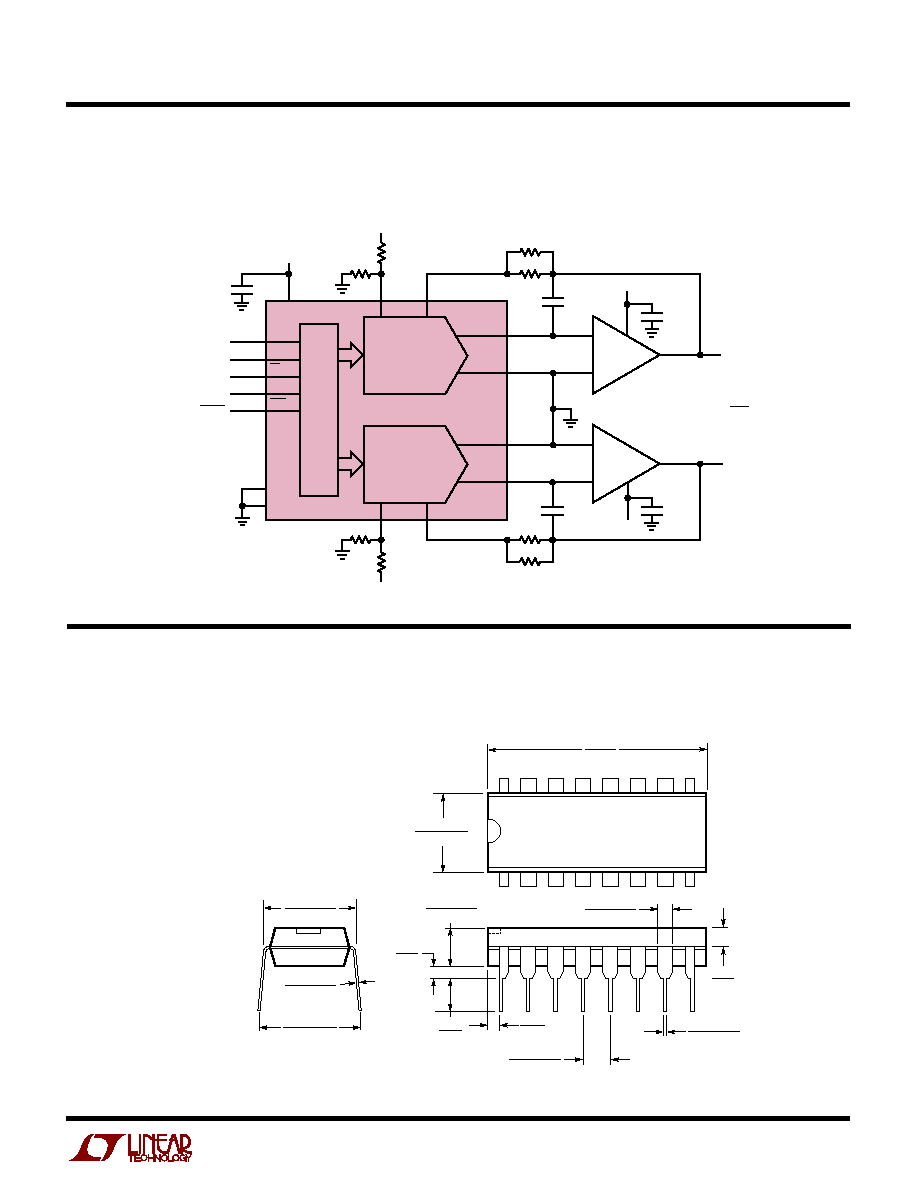
N Package
16-Lead PDIP (Narrow 0.300)
(LTC DWG # 05-08-1510)
12
LTC1590
©
LINEAR TECHNOLOGY CORPORATION 1997
1590f LT/TP 1197 4K ∑ PRINTED IN USA
Linear Technology Corporation
1630 McCarthy Blvd., Milpitas, CA 95035-7417
q
(408) 432-1900
FAX: (408) 434-0507
q
TELEX: 499-3977
q
www.linear-tech.com
Dimensions in inches (millimeters) unless otherwise noted.
PACKAGE DESCRIPTIO
N
U
S Package
16-Lead Plastic Small Outline (Narrow 0.150)
(LTC DWG # 05-08-1610)
0.016 ≠ 0.050
0.406 ≠ 1.270
0.010 ≠ 0.020
(0.254 ≠ 0.508)
◊
45
į
0
į
≠ 8
į
TYP
0.008 ≠ 0.010
(0.203 ≠ 0.254)
S16 0695
1
2
3
4
5
6
7
8
0.150 ≠ 0.157**
(3.810 ≠ 3.988)
16
15
14
13
0.386 ≠ 0.394*
(9.804 ≠ 10.008)
0.228 ≠ 0.244
(5.791 ≠ 6.197)
12
11
10
9
0.053 ≠ 0.069
(1.346 ≠ 1.752)
0.014 ≠ 0.019
(0.355 ≠ 0.483)
0.004 ≠ 0.010
(0.101 ≠ 0.254)
0.050
(1.270)
TYP
DIMENSION DOES NOT INCLUDE MOLD FLASH. MOLD FLASH
SHALL NOT EXCEED 0.006" (0.152mm) PER SIDE
DIMENSION DOES NOT INCLUDE INTERLEAD FLASH. INTERLEAD
FLASH SHALL NOT EXCEED 0.010" (0.254mm) PER SIDE
*
**
Dual Programmable Attenuator with Gain
TYPICAL APPLICATIO
N
U
PART NUMBER
DESCRIPTION
COMMENTS
LTC1595
16-Bit Multiplying I
OUT
DAC in SO-8
True 16-Bit Upgrade for DAC8043
LTC1596
16-Bit Multiplying I
OUT
DAC
True 16-Bit Upgrade for DAC8143 and AD7543
LTC7541A
Parallel I/O Multiplying I
OUT
12-Bit DAC
12-Bit Wide Parallel Input
LTC7543/LTC8143
Serial I/O Multiplying I
OUT
12-Bit DACs
Clear Pin and Serial Data Output (LTC8143)
LTC7545A
Parallel I/O Multiplying I
OUT
12-Bit DAC
12-Bit Wide Latched Parallel Input
LTC8043
Serial I/O Multiplying I
OUT
12-Bit DAC
8-Pin SO and PDIP
RELATED PARTS
13
14
11
12
15
DATA IN
SERIAL CLOCK
CHIP SELECT/DAC LOAD
DATA OUT
CLEAR
16
9
8
1
15k
2
10
1590 TA10
3
5
7
1
8
6
4
5
6
2
3
4
V
OUT B
V
OUT A
5V
1k
V
IN B
Ī
10V
7
33pF
0.1
Ķ
F
0.01
Ķ
F
33pF
15V
≠15V
0.01
Ķ
F
V
OUT
= ≠V
IN
16D
4096
( )
15k
15k
1k
1k
15k
1k
V
IN A
Ī
10V
DAC B
V
REF B
R
FB B
V
REF A
R
FB A
DAC A
24-BIT
SHIFT
REG
AND
LATCH
D
IN
CLK
CS/LD
D
OUT
CLR
DGND
AGND
LTC1590
OUT1 B
OUT2 B
OUT2 A
OUT1 A
+
≠
+
≠
1/2
LT1358
1/2
LT1358