 | ÐлекÑÑоннÑй компоненÑ: LTC1609 | СкаÑаÑÑ:  PDF PDF  ZIP ZIP |
1609fa.pm6
1
LTC1609
1609fa
1
2
3
4
5
6
7
8
9
10
11
12
13
14
LTC1609
28
27
26
25
24
23
22
21
20
19
18
17
16
15
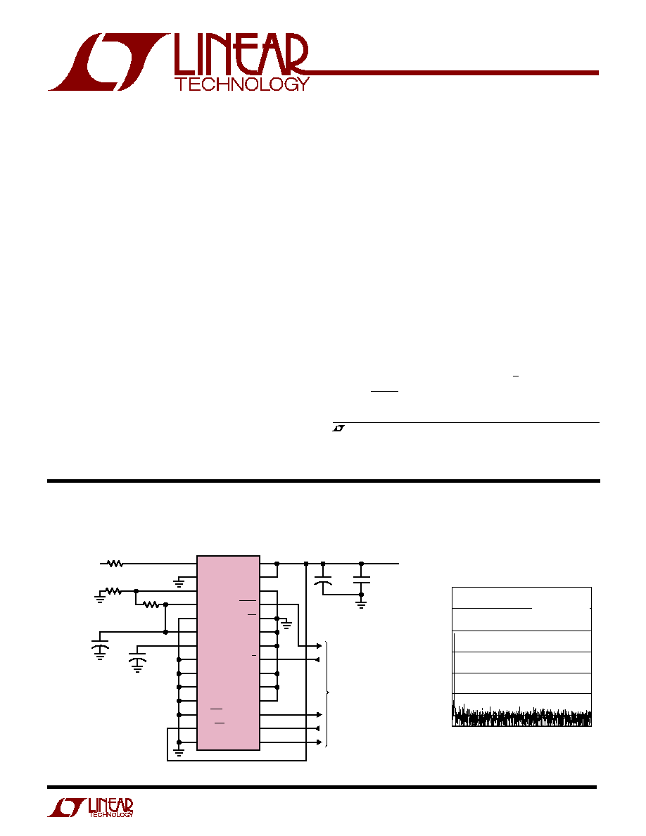
R1
IN
AGND1
R2
IN
R3
IN
NC
CAP
REF
NC
AGND2
NC
NC
SB/BTC
EXT/INT
DGND
V
DIG
V
ANA
PWRD
BUSY
CS
NC
NC
R/C
NC
TAG
NC
DATA
DATACLK
SYNC
+
33.2k
0.1
µ
F
100
ANALOG INPUT
10V TO 10V
2.2
µ
F
+
2.2
µ
F
+
10
µ
F
SERIAL INTERFACE
1609 TA01
5V
200
2.5V
2.5V
The LTC
®
1609 is a 200ksps, serial sampling 16-bit A/D
converter that draws only 65mW (typical) from a single 5V
supply. This easy-to-use device includes a sample-and-
hold, a precision reference, a switched capacitor succes-
sive approximation A/D and trimmed internal clock.
The input range is specified for bipolar inputs of
±
10V,
±
5V and
±
3.3V and unipolar inputs of 0V to 10V, 0V to 5V
and 0V to 4V. Maximum DC specs include
±
2LSB INL and
16-bit no missing codes over temperature. It has a typical
signal-to-noise ratio of 87dB.
The ADC has a high speed serial interface. The serial
output data can be clocked out using either the internal
serial shift clock or be clocked out by an external shift
clock. A separate convert start input (R/C) and a data ready
signal (BUSY) ease connections to FIFOs, DSPs and
microprocessors.
16-Bit, 200ksps, Serial ADC
with Multiple Input Ranges
s
Sample Rate: 200ksps
s
Input Ranges
Unipolar: 0V to 10V, 0V to 5V and 0V to 4V
Bipolar:
±
10V,
±
5V and
±
3.3V
s
Guaranteed No Missing Codes
s
Serial I/O
s
Single 5V Supply
s
Power Dissipation: 65mW Typ
s
Power Down Mode: 50
µ
W
s
SNR: 87dB Typ
s
Operates with Internal or External Reference
s
28-Pin SSOP and 20-Pin SO Packages
s
Improved 2nd Source to ADS7809 and AD977A
s
Industrial Process Control
s
Multiplexed Data Acquisition Systems
s
High Speed Data Acquisition for PCs
s
Digital Signal Processing
200kHz, 16-Bit Serial Sampling ADC Configured for
±
10V Inputs
, LTC and LT are registered trademarks of Linear Technology Corporation.
DESCRIPTIO
U
FEATURES
APPLICATIO S
U
TYPICAL APPLICATIO
U
FREQUENCY (kHz)
0
60
40
0
75
1609 G06
80
100
25
50
100
120
130
20
MAGNITUDE (dB)
f
SAMPLE
= 200kHz
f
IN
= 1kHz
SINAD = 87.2dB
THD = 100.1dB
Nonaveraged 4096 Point FFT Plot
2
LTC1609
1609fa
(Notes 1, 2)
V
ANA
.......................................................................... 7V
V
DIG
to V
ANA
........................................................... 0.3V
V
DIG
........................................................................... 7V
Ground Voltage Difference
DGND, AGND1 and AGND2 ..............................
±
0.3V
Analog Inputs (Note 3)
R1
IN
, R2
IN
, R3
IN
................................................
±
25V
CAP ............................ V
ANA
+ 0.3V to AGND2 0.3V
REF .................................... Indefinite Short to AGND2
Momentary Short to V
ANA
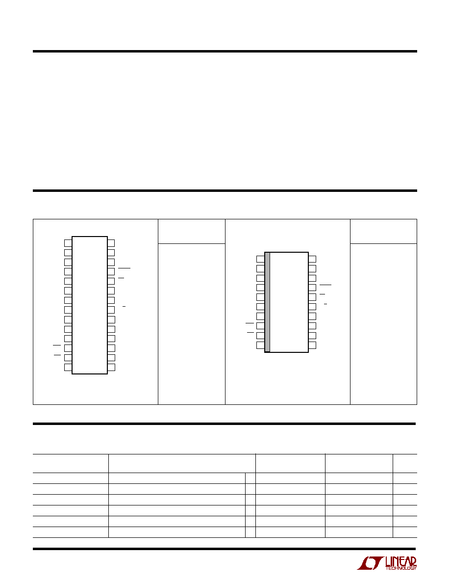
ABSOLUTE
M
AXI
M
U
M
RATINGS
W
W
W
U
PACKAGE/ORDER I
N
FOR
M
ATIO
N
W
U
U
ORDER PART
NUMBER
LTC1609CG
LTC1609IG
T
JMAX
= 125
°
C,
JA
= 95
°
C/W
1
2
3
4
5
6
7
8
9
10
11
12
13
14
TOP VIEW
G PACKAGE
28-LEAD PLASTIC SSOP
28
27
26
25
24
23
22
21
20
19
18
17
16
15
R1
IN
AGND1
R2
IN
R3
IN
NC
CAP
REF
NC
AGND2
NC
NC
SB/BTC
EXT/INT
DGND
V
DIG
V
ANA
PWRD
BUSY
CS
NC
NC
R/C
NC
TAG
NC
DATA
DATACLK
SYNC
Consult LTC Marketing for parts specified with wider operating temperature ranges.
Digital Input Voltage (Note 4) ........ DGND 0.3V to 10V
Digital Output Voltage ........ DGND 0.3V to V
DIG
+ 0.3V
Power Dissipation .............................................. 500mW
Operating Ambient Temperature Range
LTC1609AC/LTC1609C ............................ 0
°
C to 70
°
C
LTC1609AI/LTC1609I ......................... 40
°
C to 85
°
C
Storage Temperature Range ................. 65
°
C to 150
°
C
Lead Temperature (Soldering, 10 sec).................. 300
°
C
ORDER PART
NUMBER
LTC1609CSW
LTC1609ISW
LTC1609ACSW
LTC1609AISW
1
2
3
4
5
6
7
8
9
10
TOP VIEW
SW PACKAGE
20-LEAD PLASTIC SO
20
19
18
17
16
15
14
13
12
11
R1
IN
AGND1
R2
IN
R3
IN
CAP
REF
AGND2
SB/BTC
EXT/INT
DGND
V
DIG
V
ANA
PWRD
BUSY
CS
R/C
TAG
DATA
DATACLK
SYNC
T
JMAX
= 125
°
C,
JA
= 130
°
C/W
The
q
indicates specifications which apply over the full operating
temperature range, otherwise specifications are at T
A
= 25
°
C. With external reference (Notes 5, 6).
LTC1609
LTC1609A
PARAMETER
CONDITIONS
MIN
TYP
MAX
MIN
TYP
MAX
UNITS
Resolution
q
16
16
Bits
No Missing Codes
q
15
16
Bits
Transition Noise
0.9
0.9
LSB
RMS
Integral Linearity Error
(Note 7)
q
±
3
±
2
LSB
Differential Linearity Error
q
2
3
1
1.75
LSB
Bipolar Zero Error
External Reference = 2.5V (Note 8), Bipolar Ranges
q
±
10
±
10
mV
CO
N
VERTER CHARACTERISTICS
U
3
LTC1609
1609fa
LTC1609
LTC1609A
SYMBOL
PARAMETER
CONDITIONS
MIN
TYP
MAX
MIN
TYP
MAX
UNITS
S/(N + D)
Signal-to-(Noise
1kHz Input Signal (Note 14)
87.5
85
87.5
dB
+ Distortion) Ratio
10kHz Input Signal
87
87
dB
20kHz, 60dB Input Signal
30
30
dB
THD
Total Harmonic
1kHz Input Signal, First 5 Harmonics
100
100
96
dB
Distortion
10kHz Input Signal, First 5 Harmonics
94
94
dB
Peak Harmonic or
1kHz Input Signal
102
102
dB
Spurious Noise
10kHz Input Signal
94
94
dB
Full-Power Bandwidth
(Note 15)
275
275
kHz
3dB Input Bandwidth
1
1
MHz
Aperture Delay
40
40
ns
Aperture Jitter
Sufficient to Meet AC Specs Sufficient to Meet AC Specs
Transient Response
Full-Scale Step (Note 9)
2
2
µ
s
Overvoltage Recovery
(Note 16)
150
150
ns
LTC1609/LTC1609A
SYMBOL
PARAMETER
CONDITIONS
MIN
TYP
MAX
UNITS
V
IN
Analog Input Range (Note 9)
4.75V
V
ANA
5.25V, 4.75V
V
DIG
5.25V,
q
±
10, 0V to 5V, etc.
V
(See Tables 1a and 1b)
C
IN
Analog Input Capacitance
10
pF
R
IN
Analog Input Impedance
See Tables 1a and 1b
k
The
q
indicates specifications which apply over the full operating temperature range,
otherwise specifications are at T
A
= 25
°
C. (Note 5)
(Notes 5, 14)
A ALOG I PUT
U
U
DY
A
IC ACCURACY
U
W
LTC1609/LTC1609A
PARAMETER
CONDITIONS
MIN
TYP
MAX
UNITS
V
REF
Output Voltage
I
OUT
= 0
q
2.470
2.500
2.520
V
V
REF
Output Tempco
I
OUT
= 0
±
5
ppm/
°
C
Internal Reference Source Current
1
µ
A
External Reference Voltage for Specified Linearity
(Notes 9, 10)
2.30
2.50
2.70
V
External Reference Current Drain
External Reference = 2.5V (Note 9)
q
100
µ
A
CAP Output Voltage
I
OUT
= 0
2.50
V
The
q
indicates specifications which apply over the full
operating temperature range, otherwise specifications are at T
A
= 25
°
C. (Note 5)
I
N
TER
N
AL REFERE
N
CE CHARACTERISTICS
U
U
U
The
q
indicates specifications which apply over the full operating
temperature range, otherwise specifications are at T
A
= 25
°
C. With external reference (Notes 5, 6).
LTC1609
LTC1609A
PARAMETER
CONDITIONS
MIN
TYP
MAX
MIN
TYP
MAX
UNITS
Bipolar Zero Error Drift
Bipolar Ranges
±
2
±
2
ppm/
°
C
Unipolar Zero Error
External Reference = 2.5V, Unipolar Ranges
q
±
10
±
10
mV
Unipolar Zero Error Drift
Unipolar Ranges
±
2
±
2
ppm/
°
C
Full-Scale Error Drift
±
7
±
7
ppm/
°
C
Full-Scale Error
External Reference = 2.5V (Notes 12, 13)
q
±
0.50
±
0.25
%
Full-Scale Error Drift
External Reference = 2.5V
±
2
±
2
ppm/
°
C
Power Supply Sensitivity
V
ANA
= V
DIG
= V
DD
V
DD
= 5V
±
5% (Note 9)
±
8
±
8
LSB
CO
N
VERTER CHARACTERISTICS
U
4
LTC1609
1609fa
LTC1609/LTC1609A
SYMBOL
PARAMETER
CONDITIONS
MIN
TYP
MAX
UNITS
V
IH
High Level Input Voltage
V
DD
= 5.25V
q
2.4
V
V
IL
Low Level Input Voltage
V
DD
= 4.75V
q
0.8
V
I
IN
Digital Input Current
V
IN
= 0V to V
DD
q
±
10
µ
A
C
IN
Digital Input Capacitance
5
pF
V
OH
High Level Output Voltage
V
DD
= 4.75V
I
O
= 10
µ
A
4.5
V
I
O
= 200
µ
A
q
4.0
V
V
OL
Low Level Output Voltage
V
DD
= 4.75V
I
O
= 160
µ
A
0.05
V
I
O
= 1.6mA
q
0.10
0.4
V
I
SOURCE
Output Source Current
V
OUT
= 0V
10
mA
I
SINK
Output Sink Current
V
OUT
= V
DD
10
mA
The
q
indicates specifications which apply over the full
operating temperature range, otherwise specifications are at T
A
= 25
°
C. (Note 5)
DIGITAL I PUTS A D DIGITAL OUTPUTS
U
U
LTC1609/LTC1609A
SYMBOL
PARAMETER
CONDITIONS
MIN
TYP
MAX
UNITS
t
1
Convert Pulse Width
(Note 11)
q
40
ns
t
2
R/C, CS to BUSY Delay
C
L
= 25pF
q
80
ns
t
3
BUSY Low Time
q
3
µ
s
t
4
BUSY Delay After End of Conversion
100
ns
t
5
Aperture Delay
5
ns
t
6
Conversion Time
q
3
µ
s
t
7
Acquisition Time
q
2
µ
s
t
6
+ t
7
Throughput Time
q
5
µ
s
t
8
R/C Low to DATACLK Delay
260
ns
t
9
DATACLK Period
150
ns
t
10
DATA Valid Setup Time
q
15
ns
t
11
DATA Valid Hold Time
q
40
ns
t
12
External DATACLK Period
q
50
ns
t
13
External DATACLK High
q
20
ns
t
14
External DATACLK Low
q
20
ns
t
15
R/C, CS to External DATACLK Setup Time
q
15
t
12
ns
t
16
R/C to CS Setup Time
q
10
ns
t
17
External DATACLK to SYNC Delay
q
6
50
ns
t
18
External DATACLK to DATA Valid Delay
q
10
50
ns
t
19
CS to External DATACLK Rising Edge Delay
q
10
ns
t
20
Previous DATA Valid After CS, R/C Low
(Note 9)
q
2.2
µ
s
t
21
BUSY to External DATACLK Setup Time
(Note 9)
q
5
ns
t
22
BUSY Falling Edge to Final External DATACLK
(Notes 10, 17)
q
1.2
µ
s
t
23
TAG Valid Setup Time
q
0
ns
t
24
TAG Valid Hold Time
q
15
ns
The
q
indicates specifications which apply over the full operating temperature
range, otherwise specifications are at T
A
= 25
°
C. (Note 5)
TI I G CHARACTERISTICS
U
W

5
LTC1609
1609fa
Note 1: Absolute Maximum Ratings are those values beyond which the life
of a device may be impaired.
Note 2: All voltage values are with respect to ground with DGND, AGND1
and AGND2 wired together (unless otherwise noted).
Note 3: When these pin voltages are taken below ground or above V
ANA
=
V
DIG
= V
DD
, they will be clamped by internal diodes. This product can
handle input currents of greater than 100mA below ground or above V
DD
without latch-up.
Note 4: When these pin voltages are taken below ground, they will be
clamped by internal diodes. This product can handle input currents of
90mA below ground without latchup. These pins are not clamped to V
DD
.
Note 5: V
DD
= 5V, f
SAMPLE
= 200kHz, t
r
= t
f
= 5ns unless otherwise
specified.
Note 6: Linearity, offset and full-scale specifications apply for a V
IN
input
with respect to ground.
Note 7: Integral nonlinearity is defined as the deviation of a code from a
straight line passing through the actual end points of the transfer curve.
The deviation is measured from the center of the quantization band.
Note 8: Bipolar zero error is the offset voltage measured from 0.5 LSB
when the output code flickers between 0000 0000 0000 0000 and 1111
1111 1111 1111. Unipolar zero error is the offset voltage measured from
0.5LSB when the output codes flickers between 0000. . .0000 and 0000. .
.0001.
Note 9: Guaranteed by design, not subject to test.
Note 10: Recommended operating conditions.
Note 11: With CS low the falling R/C edge starts a conversion. If R/C
returns high at a critical point during the conversion it can create small
errors. For best results ensure that R/C returns high within 1.2
µ
s after the
start of the conversion.
Note 12: As measured with fixed 1% resistors shown in Figures 3a and
3b. Adjustable to zero with external potentiometer.
Note 13: Full-scale error is the worst-case of FS or +FS untrimmed
deviation from ideal first and last code transitions, divided by the transition
voltage (not divided by the full-scale range) and includes the effect of
offset error. For unipolar input ranges full-scale error is the deviation of
the last code transition from ideal divided by the transiton voltage and
includes the effect of offset error.
Note 14: All specifications in dB are referred to a full-scale
±
5V input.
Note 15: Full-power bandwidth is defined as full-scale input frequency at
which a signal-to-(noise + distortion) degrades to 60dB or 10 bits of
accuracy.
Note 16: Recovers to specified performance after (2
· FS) input
overvoltage.
Note 17: When data is shifted out during a conversion, with an external
data clock, complete the process within 1.2
µ
s from the start of the
conversion (BUSY falling). This will help keep any external disturbances
from causing an error in the conversion result.
POWER REQUIRE
M
E
N
TS
W
U
LTC1609/LTC1609A
SYMBOL
PARAMETER
CONDITIONS
MIN
TYP
MAX
UNITS
V
DD
Positive Supply Voltage
(Notes 9, 10)
4.75
5.25
V
I
DD
Positive Supply Current
PWRD = Low
q
13
20
mA
P
DIS
Power Dissipation
PWRD = Low
65
100
mW
PWRD = High
50
µ
W
The
q
indicates specifications which apply over the full operating temperature range,
otherwise specifications are at T
A
= 25
°
C. (Note 5)