 | –≠–ª–µ–∫—Ç—Ä–æ–Ω–Ω—ã–π –∫–æ–º–ø–æ–Ω–µ–Ω—Ç: LTC1654 | –°–∫–∞—á–∞—Ç—å:  PDF PDF  ZIP ZIP |
1
LTC1654
1654fa
Dual 14-Bit Rail-to-Rail DAC
in 16-Lead SSOP Package
s
14-Bit Monotonic Over Temperature
s
Smallest Dual 14-Bit DAC: 16-Lead Narrow
SSOP Package
s
Individually Programmable Speed/Power:
3.5
µ
s Settling Time at 750
µ
A
8
µ
s Settling Time at 450
µ
A
s
3V to 5V Single Supply Operation
s
Maximum Update Rate: 0.9MHz
s
Buffered True Rail-to-Rail Voltage Outputs
s
User Selectable Gain
s
Power-On Reset and Clear Function
s
Schmitt Trigger On Clock Input Allows Direct
Optocoupler Interface
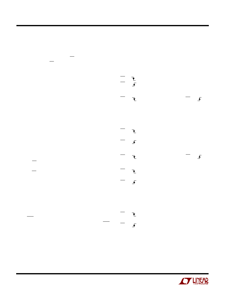
The LTC
Æ
1654 is a dual, rail-to-rail voltage output, 14-bit
digital-to-analog converter (DAC). It is available in a
16-lead narrow SSOP package, making it the smallest dual
14-bit DAC available. It includes output buffer amplifiers
and a flexible serial interface.
The LTC1654 has REFHI pins for each DAC that can be
driven up to V
CC
. The output will swing from 0V to V
CC
in
a gain of 1 configuration or V
CC
/2 in a gain of 1/2 configu-
ration. It operates from a single 2.7V to 5.5V supply.
The LTC1654 has two programmable speeds: a FAST and
SLOW mode with
±
1LSB settling times of 3.5
µ
s or 8
µ
s
respectively and supply currents of 750
µ
A and 450
µ
A in
the two modes. The LTC1654 also has shutdown capabil-
ity, power-on reset and a clear function to 0V.
s
Digital Calibration
s
Industrial Process Control
s
Automatic Test Equipment
s
Offset/Gain Adjustment
s
Multiplying DAC
, LTC and LT are registered trademarks of Linear Technology Corporation.
DAC B
1654 BD
V
OUT B
REFHI B
V
OUT A
X
1
/X
1/2
B
REFHI A
≠
+
POWER-ON
RESET
DAC A
REFLO A
REFLO B
X
1
/X
1/2
A
≠
+
INPUT
LATCH
CONTROL
LOGIC
CS/LD
SCK
SDO
CLR
SDI
INPUT
LATCH
DAC
REGISTER
32-BIT
SHIFT
REGISTER
DAC
REGISTER
FEATURES
DESCRIPTIO
U
APPLICATIO S
U
BLOCK DIAGRA
W

2
LTC1654
1654fa
(Note 1)
V
CC
to GND .............................................. ≠ 0.5V to 7.5V
TTL Input Voltage, REFHI,
REFLO, X
1
/X
1/2
........................................ ≠ 0.5V to 7.5V
V
OUT
, SDO .................................. ≠ 0.5V to (V
CC
+ 0.5V)
Operating Temperature Range
LTC1654C ............................................. 0
∞
C to 70
∞
C
LTC1654I ........................................ ≠ 40
∞
C to 85
∞
C
Maximum Junction Temperature .......................... 125
∞
C
Storage Temperature Range ................ ≠ 65
∞
C to 150
∞
C
Lead Temperature (Soldering, 10 sec)................. 300
∞
C
ORDER PART
NUMBER
T
JMAX
= 125
∞
C,
JA
= 110
∞
C/W
LTC1654CGN
LTC1654IGN
The
q
denotes specifications which apply over the full operating tempera-
ture range, otherwise specifications are at T
A
= 25
∞
C, V
CC
= 2.7V to 5.5V, V
OUT A
, V
OUT B
unloaded, REFHI A, REFHI B = 4.096V
(V
CC
= 5V), REFHI A, REFHI B = 2.048V (V
CC
= 2.7V), REFLO = 0V, X
1
/X
1/2
= 0V.
GN PACKAGE
16-LEAD PLASTIC SSOP
1
2
3
4
5
6
7
8
TOP VIEW
16
15
14
13
12
11
10
9
X
1
/X
1/2
B
CLR
SCK
SDI
CS/LD
DGND
SDO
X
1
/X
1/2
A
V
CC
V
OUT B
REFHI B
REFLO B
AGND
REFLO A
REFHI A
V
OUT A
GN PART MARKING
1654
1654I
SYMBOL
PARAMETER
CONDITIONS
MIN
TYP
MAX
UNITS
DAC
Resolution
q
14
Bits
Monotonicity
q
14
Bits
DNL
Differential Nonlinearity
Guaranteed Monotonic (Note 2)
q
±
0.3
±
1
LSB
INL
Integral Nonlinearity
Integral Nonlinearity (Note 2)
q
±
1.2
±
4
LSB
ZSE
Zero Scale Error
0
∞
C
T
A
70
∞
C
q
0
6.5
mV
≠ 40
∞
C
T
A
85
∞
C
q
9.0
mV
V
OS
Offset Error
0
∞
C
T
A
70
∞
C (Note 3)
q
±
6.5
mV
≠ 40
∞
C
T
A
85
∞
C (Note 3)
q
±
9.0
mV
V
OS
TC
Offset Error Tempco
±
15
µ
V/
∞
C
Gain Error
q
±
24
LSB
Gain Error Drift
5
ppm/
∞
C
Power Supply
V
CC
Positive Supply Voltage
For Specified Performance
q
2.7
5.5
V
I
CC
Supply Current (SLOW/FAST)
2.7V
V
CC
5.5V (Note 5) SLOW
q
450
800
µ
A
2.7V
V
CC
5.5V (Note 5) FAST
q
750
1300
µ
A
2.7V
V
CC
3.3V (Note 5) SLOW
q
250
500
µ
A
2.7V
V
CC
3.3V (Note 5) FAST
q
450
900
µ
A
In Shutdown (Note 5)
q
7
30
µ
A
Op Amp DC Performance
Short-Circuit Current Low
V
OUT
Shorted to GND
q
70
120
mA
Short-Circuit Current High
V
OUT
Shorted to V
CC
q
80
120
mA
Output Impedance to GND
Input Code = 0
q
40
200
Output Line Regulation
Input Code = 16383, V
CC
= 2.7V to 5.5V,
q
2.25
mV/V
V
REF
= 2.048V
ABSOLUTE AXI U RATI GS
W
W
W
U
PACKAGE/ORDER I FOR ATIO
U
U
W
ELECTRICAL CHARACTERISTICS
Consult LTC Marketing for parts specified with wider operating temperature ranges.
3
LTC1654
1654fa
The
q
denotes specifications which apply over the full operating tempera-
ture range, otherwise specifications are at T
A
= 25
∞
C, V
CC
= 2.7V to 5.5V, V
OUT A
, V
OUT B
unloaded, REFHI A, REFHI B = 4.096V
(V
CC
= 5V), REFHI A, REFHI B = 2.048V (V
CC
= 2.7V), REFLO = 0V, X
1
/X
1/2
= 0V.
SYMBOL
PARAMETER
CONDITIONS
MIN
TYP
MAX
UNITS
AC Performance
Voltage Output Slew Rate
(Note 8) SLOW
q
0.20
V/
µ
s
(Note 8) FAST
q
1.25
V/
µ
s
Voltage Output Settling Time
(Note 4) to
±
1LSB, SLOW
8.0
µ
s
(Note 4) to
±
1LSB, FAST
3.5
µ
s
Digital Feedthrough
(Note 7)
1
nV∑s
Midscale Glitch Impulse
DAC Switch Between 8000 and 7FFF
20
nV∑s
Output Noise Voltage Density
at 10kHz, SLOW
260
nV/
Hz
at 10kHz, FAST
180
nV/
Hz
Digital I/O
V
IH
Digital Input High Voltage
V
CC
= 5V
q
2.4
V
V
IL
Digital Input Low Voltage
V
CC
= 5V
q
0.8
V
V
OH
Digital Output High Voltage
V
CC
= 5V, I
OUT
= ≠ 1mA, D
OUT
Only
q
V
CC
≠ 0.75
V
V
OL
Digital Output Low Voltage
V
CC
= 5V, I
OUT
= 1mA, D
OUT
Only
q
0.4
V
V
IH
Digital Input High Voltage
V
CC
= 3V
q
2.4
V
V
IL
Digital Input Low Voltage
V
CC
= 3V
q
0.8
V
V
OH
Digital Output High Voltage
V
CC
= 3V, I
OUT
= ≠ 1mA, D
OUT
Only
q
V
CC
≠ 0.75
V
V
OL
Digital Output Low Voltage
V
CC
= 3V, I
OUT
= 1mA, D
OUT
Only
q
0.4
V
I
LEAK
Digital Input Leakage
V
IN
= GND to V
CC
q
±
10
µ
A
C
IN
Digital Input Capacitance
(Note 6)
10
pF
Reference Input
Reference Input Resistance
REFHI to REFLO
q
30
60
k
Reference Input Range
(Note 6)
q
0
V
CC
V
Reference Input Current
In Shutdown
q
1
µ
A
Switching Characteristics (V
CC
= 4.5V to 5.5V)
t
1
SDI Valid to SCK Setup
q
30
ns
t
2
SDI Valid to SCK Hold
(Note 6)
q
0
ns
t
3
SCK High Time
(Note 6)
q
15
ns
t
4
SCK Low Time
(Note 6)
q
15
ns
t
5
CS/LD Pulse Width
(Note 6)
q
15
ns
t
6
LSB SCK to CS/LD
(Note 6)
q
10
ns
t
7
CS/LD Low to SCK
(Note 6)
q
10
ns
t
8
SD0 Output Delay
C
LOAD
= 100pF
q
5
100
ns
t
9
SCK Low to CS/LD Low
(Note 6)
q
10
ns
Switching Characteristics (V
CC
= 2.7V to 5.5V)
t
1
SDI Valid to SCK Setup
q
45
ns
t
2
SDI Valid to SCK Hold
(Note 6)
q
0
ns
t
3
SCK High Time
(Note 6)
q
20
ns
t
4
SCK Low Time
(Note 6)
q
20
ns
t
5
CS/LD Pulse Width
(Note 6)
q
20
ns
t
6
LSB SCK to CS/LD
(Note 6)
q
15
ns
t
7
CS/LD Low to SCK
(Note 6)
q
15
ns
t
8
SDO Output Delay
C
LOAD
= 100pF
q
5
150
ns
t
9
SCK Low to CS/LD Low
(Note 6)
q
15
ns
ELECTRICAL CHARACTERISTICS

4
LTC1654
1654fa
V
OUT
).
Note 4: DAC switched between code 212 and code 16383.
Note 5: Digital inputs at 0V or V
CC
.
Note 6: Guaranteed by design.
Note 7: CS/LD = 0, V
OUT
= 4.096V and data is being clocked in.
Note 8: 100pF load capacitor.
Note 1: Absolute Maximum Ratings are those values beyond which the life
of a device may be impaired.
Note 2: Nonlinearity is defined from "start code" 142 to code 16383 with a
gain of 1(X
1
/X
1/2
= REFLO) and from "start code" 212 to code 16383 with
a gain of 1/2(X
1
/X
1/2
= V
OUT
). See Applications Information.
Note 3: Offset error is measured at "start code" 142 for a gain = 1(X
1
/X
1/2
= REFLO) and measured at "start code" 212 for a gain = 1/2( X
1
/X
1/2
=
ELECTRICAL CHARACTERISTICS
TYPICAL PERFOR A CE CHARACTERISTICS
U
W
Integral Nonlinearity (INL)
vs Input Code
INPUT CODE
0
INL (LSB)
0
0.5
1.0
16383
1654 G01
≠0.5
≠1.0
≠2.0
8192
≠1.5
2.0
1.5
INPUT CODE
0
DNL (LSB)
0
0.5
1.0
16383
1654 G02
≠0.5
≠1.0
≠2.0
8192
≠1.5
2.0
1.5
TEMPERATURE (
∞
C)
≠55
OFFSET ERROR (mV)
≠1.25
1.25
125
1654 G03
≠2.50
≠25
5
35
65
95
2.50
0
Differential Nonlinearity (DNL)
vs Input Code
Offset vs Temperature
Gain Error vs Temperature
Minimum Output Voltage
vs Load Current (Output Sinking)
Minimum Supply Headroom vs
Load Current (Output Sourcing)
TEMPERATURE (
∞
C)
≠55
GAIN ERROR (LSB)
≠2.5
2.5
125
1654 G04
≠5.0
≠25
5
35
65
95
5.0
0
OUTPUT SINK CURRENT (mA)
0
OUTPUT PULL-DOWN VOLTAGE (V)
0.6
0.8
1.0
10
1645 G05
0.4
0.2
0.5
0.7
0.9
0.3
0.1
0
5
15
CODE: ALL ZEROS
T
A
= 125
∞
C
T
A
= 25
∞
C
T
A
= ≠55
∞
C
LOAD CURRENT (mA)
0
V
CC
≠ V
OUT
(V)
0.6
0.8
1.0
10
1645 G06
0.4
0.2
0.5
0.7
0.9
0.3
0.1
0
5
15
T
A
= 125
∞
C
CODE: ALL 1s
V
REFHI
= 4.096V
T
A
= 25
∞
C
T
A
= ≠55
∞
C

5
LTC1654
1654fa
TYPICAL PERFOR A CE CHARACTERISTICS
U
W
Supply Current
vs Logic Input Voltage
Large-Signal Settling--Fast Mode
LOGIC INPUT VOLTAGE (V)
0
SUPPLY CURRENT (mA)
1.5
3.0
4
1654 G07
0
1
2
3
5
Large-Signal Settling--Slow Mode
Midscale Glitch--Fast Mode
Midscale Glitch--Slow Mode
V
OUT
Glitch at Power-Up
V
OUT
10mV/DIV
CS/LD
2V/DIV
TIME (1
µ
s/DIV)
1654 G10
V
OUT
10mV/DIV
CS/LD
2V/DIV
TIME (1
µ
s/DIV)
1654 G11
V
CC
0.5V/DIV
TIME (50ms/DIV)
1654 G12
V
OUT
50mV/DIV
V
OUT
1V/DIV
CS/LD
2V/DIV
TIME (2
µ
s/DIV)
1654 G08
V
OUT
1V/DIV
CS/LD
2V/DIV
TIME (2
µ
s/DIV)
1654 G09
6
LTC1654
1654fa
CS/LD (Pin 5): The TTL Level Input for the Serial Interface
Enable and Load Control. When CS/LD is low, the SCK
signal is enabled, so the data can be clocked in. When
CS/LD is pulled high, the control/address bits are
decoded.
DGND/AGND (Pins 6, 12): Digital and Analog Grounds.
SDO (Pin 7): The output of the shift register that becomes
valid on the rising edge of the serial clock.
V
OUT A/B
(Pins 9, 15): The Buffered DAC Outputs.
REFHI A/B (Pins 10, 14): The Reference High Inputs of the
LTC1654. There is a gain of 1 from this pin to the output
in a gain of 1 configuration. In a gain of 1/2 configuration,
there is a gain of 1/2 from this pin to V
OUT
.
REFLO A/B (Pins 11, 13): The Reference Low Inputs of the
LTC1654. These inputs can swing up to V
CC
≠ 1.5V.
V
CC
(Pin 16): The Positive Supply Input. 2.7V
V
CC
5.5V.
Requires a 0.1
µ
F bypass capacitor to ground.
X
1
/X
1/2
B, X
1
/X
1/2
A (Pins 1, 8): The Gain of 1 or Gain of
1/2 Pin. When this pin is tied to V
OUT
, the output range will
be REFLO to (REFLO + REFHI)/2 (0V to REFHI/2 when
REFLO = 0V). When this pin is tied to REFLO, the output
range will be REFLO to REFHI (0V to REFHI when REFLO
= 0V). These pins should not be left floating.
CLR (Pin 2): The Asynchronous Clear Input.
SCK (Pin 3): The TTL Level Input for the Serial Interface
Clock.
SDI (Pin 4): The TTL Level Input for the Serial Interface
Data. Data on the SDI pin is latched into the shift register
on the rising edge of the serial clock. The LTC1654 allows
either a 24-bit or 32-bit word. When a 24-bit word is used,
the first 8 bits are control and address followed by 16 data
bits. The last two of the 16 data bits are don't cares. When
a 32-bit word (required for daisy-chain operation) is used,
the first 8-bits are don't cares and the following 24-bits are
as above.
1654 TD01
t
1
t
4
t
3
t
5
B0
C3
C3
X
X
X
CURRENT WORD
X
X
X
X
X
X
SCK
CS/LD
SDI
SDO
t
2
t
8
t
6
t
7
t
9
(PREVIOUS
WORD)
TI I G DIAGRA S
U
W
W
U
U
U
PI FU CTIO S
7
LTC1654
1654fa
TI I G DIAGRA S
U
W
W
1
2
3
4
5
6
7
8
9
10
11
12
13
14
15
16
17
18
19
20
21
22
23
24
C2
C1
C0
A3
A2
A1
A0
C3
CS/LD
SCK
SDI
CONTROL BITS
ADDRESS BITS
DATA WORD
24-BIT DATA STREAM
1654TD02a
B13
B12
B11
B10
B9
B8
B7
B6
B5
B4
B3
B2
B1
B0
X
X
1
2
3
4
5
6
7
8
9
10
11
12
13
14
15
16
17
18
19
20
21
22
23
24
25
26
27
28
29
30
31
32
C2
C1
C0
A3
A2
A1
A0
B13
B12
B11
B
10
B9
B8
B7
B6
B5
B4
B3
B2
B1
B0
B13
B12
B11
B10
B9
B8
B7
B6
B5
B4
B3
B2
B1
B0
XX
C3
X
X
X
X
X
X
X
X
CS/LD
SCK
SDI
CONTROL BITS
ADDRESS BITS
DATA WORD
32-BIT DATA STREAM
DON'T CARE
C2
C1
C0
A3
A2
A1
A0
XX
C3
X
X
X
X
X
X
X
X
SDO
CURRENT
STREAM
1654 TD02b
PREVIOUS STREAM
t
2
t
3
t
4
t
1
t
8
B13
17
SCK
SDI
SDO
PREVIOUS B12
PREVIOUS B13
18
B12
Figure 1a. 24-Bit Load Sequence (for Non-Daisy-Chained Applications)
Figure 1b. 32-Bit Load Sequence (for Single and Daisy-Chained LTC1654s)
8
LTC1654
1654fa
Serial Interface
The data on the SDI input is loaded into the shift register
on the rising edge of SCK. The MSB is loaded first. The
Clock is disabled internally when CS/LD is high. Note: SCK
must be low before CS/LD is pulled low to avoid an extra
internal clock pulse.
If no daisy-chaining is required, the input word can be
24-bit wide, as shown in the timing diagrams. The 8 MSBs,
which are loaded first, are the control and address bits
followed by a 16-bit data word. The last two LSBs in the
data word are don't cares. The input word can be a stream
of three 8-bit wide segments as shown in the "24-Bit
Update" timing diagram.
If daisy-chaining is required or if the input needs to be
written in two 16-bit wide segments, then the input word
can be 32 bits wide and the top 8 bits (MSBs) are don't
cares. The remaining 24 bits are control/address and data.
This is also shown in the timing diagrams. The buffered
output of the internal 32-bit shift register is available on
the SDO pin, which swings from GND to V
CC
.
Multiple LTC1654s may be daisy-chained together by
connecting the SDO pin to the SDI pin of the next IC. The
SCK and CS/LD signals remain common to all ICs in the
daisy-chain. The serial data is clocked to all of the chips,
then the CS/LD signal is pulled high to update all DACs
simultaneously.
Table 1 shows the truth table for the control/address bits.
When the supplies are first applied, the LTC1654 uses
SLOW mode, the outputs are set at 0V, and zeros are
loaded into the 32-bit input shift register. About 300ns
after power-up, the outputs are released from 0V (AGND)
and will go to the voltage on the REFLO pin.
When CLR goes active, zeros are loaded into the input and
DAC latch and the outputs are forced to AGND. After CLR
is forced high, the ouputs will go to the voltage on the
REFLO pin.
Three examples are given to illustrate the DAC's opera-
tion:
1. Load and update DAC A in FAST mode. Leave DAC B
unchanged. Perform the following sequence for the
control, address and DATA bits:
Step 1: Set DAC A in FAST mode
CS/LD
clock in 0101 0000 XXXXXXXX XXXXXXXX;
CS/LD
Step 2: Load and update DAC A with DATA
CS/LD
clock in 0011 0000 + DATA; CS/LD
2. Load and update DAC A in SLOW mode. Power down
DAC B. Perform the following sequence for the con-
trol, address and DATA bits:
Step 1: Set DAC A in SLOW mode
CS/LD
clock in 0110 0000 XXXXXXXX
XXXXXXXX;
CS/LD
Step 2: Load and update DAC A with DATA
CS/LD
clock in 0011 0000 + DATA; CS/LD
Step 3: Power down DAC B
CS/LD
clock in 0100 0001 XXXXXXXX
XXXXXXXX;
CS/LD
3. Power down both DACs at the same time. Perform the
following sequence for the control, address and DATA
bits:
Step 1: Power down both DACs simultaneously
CS/LD
clock in 0100 1111 XXXXXXXX
XXXXXXXX;
CS/LD
OPERATIO
U

9
LTC1654
1654fa
Voltage Output
The LTC1654 comes complete with rail-to-rail voltage
output buffer amplifiers. These amplifiers will swing to
within a few millivolts of either supply rail when unloaded
and to within a 450mV of either supply rail when sinking
or sourcing 5mA.
There are two GAIN configuration modes for the LTC1654:
a) GAIN of 1: (X
1
/X
1/2
tied to REFLO)
V
OUT
= (V
REFHI
≠ V
REFLO
)(CODE/16384) + V
REFLO
b) GAIN of 1/2: (X
1
/X
1/2
tied to V
OUT
)
V
OUT
= (1/2)(V
REFHI
≠ V
REFLO
)(CODE/16384) + V
REFLO
The LTC 1654 has two SPEED modes: A FAST mode and
a SLOW mode. When operating in the FAST mode, the
output amplifiers will settle in 3.5
µ
s (typ) to 14 bits on a
4V output swing. In the SLOW mode, they will settle in
8
µ
s. The total supply current is 750
µ
A in the FAST mode
and 450
µ
A in the SLOW mode. The output noise voltage
density at 10kHz is 260nV/
Hz in SLOW mode and
180nV/
Hz in FAST mode.
Power Down
Each DAC can also be independently powered down to less
than 5
µ
A/DAC of supply current. The reference pin also
goes into a high impedance state when the DAC is powered
down and the reference current will drop to below 0.1
µ
A.
The amplifiers' output stage is also three-stated but the
V
OUT
pins still have the internal gain-setting resistors
connected to them resulting in an effective resistance from
V
OUT
to REFLO. This resistance is typically 90k when the
X
1
/X
1/2
pin is tied to V
OUT
and 36k when X
1
/X
1/2
is tied to
REFLO. Because of this resistance, V
OUT
will go to V
REFLO
when the DAC is powered down and V
OUT
is unloaded.
OPERATIO
U
10
LTC1654
1654fa
OPERATIO
U
Table 1.
CONTROL
C3
C2
C1
C0
0
0
0
0
Load Input Register n
0
0
0
1
Update (Power-Up) DAC Register n
0
0
1
0
Load Input Register n, Update (Power-Up) All
0
0
1
1
Load and Update n
0
1
0
0
Power Down n
0
1
0
1
Fast n (Speed States are Maintained Even If DAC is
Put in Power-Down Mode)
0
1
1
0
Slow n (Default State is Slow When Supplies are
Powered Up)
0
1
1
1
Reserved (Do Not Use)
1
0
0
0
Reserved (Do Not Use)
1
0
0
1
Reserved (Do Not Use)
1
0
1
0
Reserved (Do Not Use)
1
0
1
1
Reserved (Do Not Use)
1
1
0
0
Reserved (Do Not Use)
1
1
0
1
Reserved (Do Not Use)
1
1
1
0
Reserved (Do Not Use)
1
1
1
1
No Operation
ADDRESS (n)
A3
A2
A1
A0
0
0
0
0
DAC A
0
0
0
1
DAC B
0
0
1
0
Reserved (Do Not Use)
0
0
1
1
Reserved (Do Not Use)
0
1
0
0
Reserved (Do Not Use)
0
1
0
1
Reserved (Do Not Use)
0
1
1
0
Reserved (Do Not Use)
0
1
1
1
Reserved (Do Not Use)
1
0
0
0
Reserved (Do Not Use)
1
0
0
1
Reserved (Do Not Use)
1
0
1
0
Reserved (Do Not Use)
1
0
1
1
Reserved (Do Not Use)
1
1
0
0
Reserved (Do Not Use)
1
1
0
1
Reserved (Do Not Use)
1
1
1
0
Reserved (Do Not Use)
1
1
1
1
Both DACs
INPUT WORD
C3
CONTROL
ADDRESS
DATA (14 + 2 DON'T CARE LSBs)
C2
C1
C0 A3 A2 A1
A0
D13 D12 D11 D10 D9
D8
D7
D6 D5
D4
D3
D2
D1
D0
X
X
1654 TABLE
11
LTC1654
1654fa
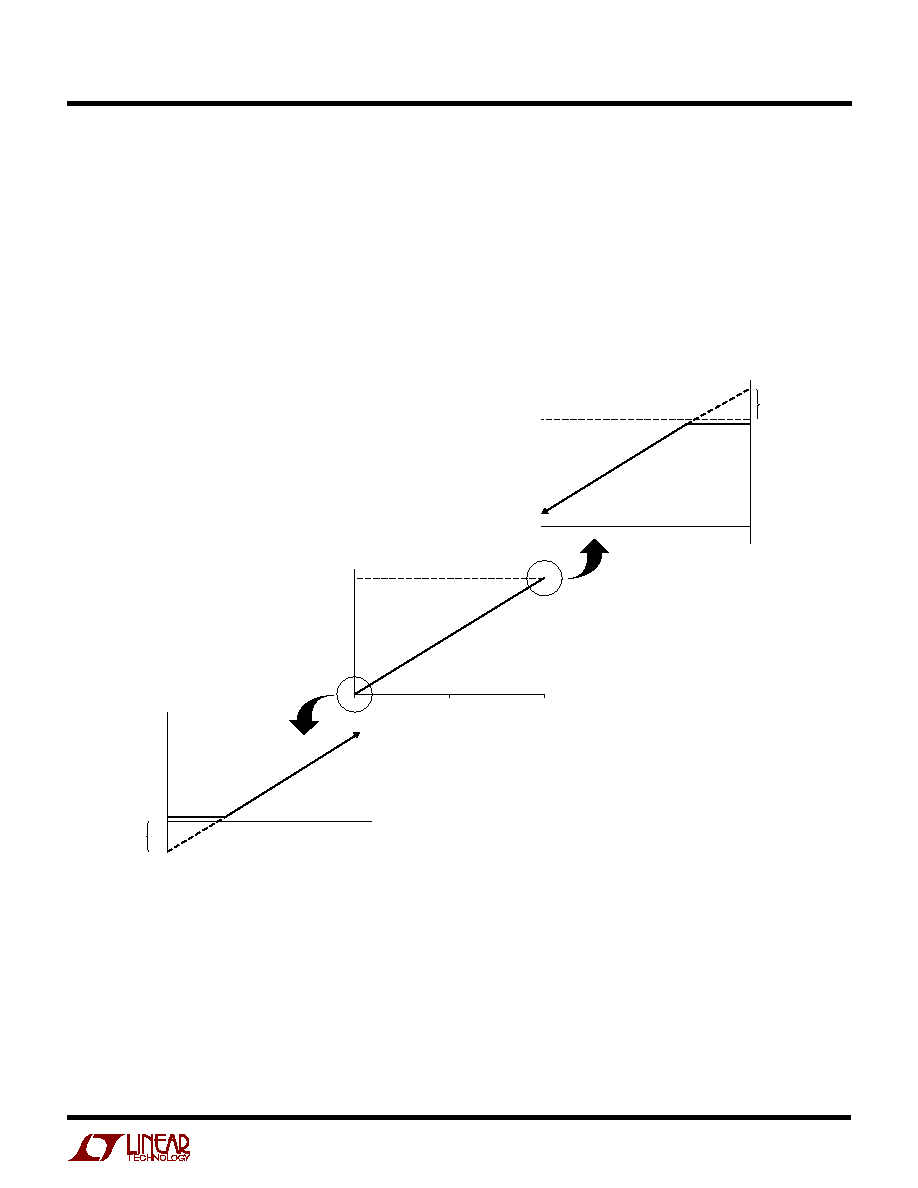
Rail-to-Rail Output Considerations
In any rail-to-rail DAC, the output swing is limited to
voltages within the supply range.
If the DAC offset is negative, the output for the lowest
codes limits at 0V as shown in Figure 2b.
Similarly, limiting can occur near full scale when the REF
pin is tied to V
CC
. If V
REF
= V
CC
and the DAC full-scale error
(FSE) is positive, the output for the highest codes limits at
V
CC
as shown in Figure 2c.
Offset and linearity are defined and tested over the region
of the DAC transfer function where no output limiting can
occur.
Figure 2. Effects of Rail-to-Rail Operation On a DAC Transfer Curve. (a) Overall Transfer Function (b) Effect of Negative
Offset for Codes Near Zero Scale (c) Effect of Positive Full-Scale Error for Input Codes Near Full Scale When V
REF
= V
CC
1654 F02
INPUT CODE
(b)
OUTPUT
VOLTAGE
NEGATIVE
OFFSET
0V
8192
0
16383
INPUT CODE
OUTPUT
VOLTAGE
(a)
V
REF
= V
CC
V
REF
= V
CC
(c)
INPUT CODE
OUTPUT
VOLTAGE
POSITIVE
FSE
APPLICATIO S I FOR ATIO
W
U
U
U
12
LTC1654
1654fa
Figure 1. Effect of Negative Offset
Least Significant Bit (LSB): One LSB is the ideal voltage
difference between two successive codes.
LSB = (V
FS
≠ V
OS
)/(2
n
≠ 1) = (V
FS
≠ V
OS
)/16383
Nominal LSBs:
LTC1654 LSB = 4.09575V/16383 = 250
µ
V
Zero-Scale Error (ZSE): The output voltage when the
DAC is loaded with all zeros. Since this is a single supply
part, this value cannot be less than 0V.
Integral Nonlinearity (INL): End-point INL is the maxi-
mum deviation from a straight line passing through the
end points of the DAC transfer curve. Because the part
operates from a single supply and the output cannot go
below zero, the linearity is measured between full scale
and a code greater than, "start code". The INL error at a
given input code is calculated as follows:
INL
= [V
OUT
≠ V
OS
≠ (V
FS
≠ V
OS
)(code/16383)]/LSB
V
OUT
= The output voltage of the DAC measured at the
given input code
Differential Nonlinearity (DNL): DNL is the difference
between the measured change and the ideal one LSB
change between any two adjacent codes. The DNL error
between any two codes is calculated as follows:
DNL
= (
V
OUT
≠ LSB)/LSB
V
OUT
= The measured voltage difference between
two adjacent codes
Digital Feedthrough: The glitch that appears at the analog
output caused by AC coupling from the digital inputs when
they change state. The area of the glitch is specified in
nV ∑ s.
Resolution (n): Resolution is defined as the number of
digital input bits (n). It is also the number of DAC output
states (2
n
) that divide the full-scale range. Resolution does
not imply linearity.
Full-Scale Voltage (V
FS
): This is the output of the DAC
when all bits are set to 1.
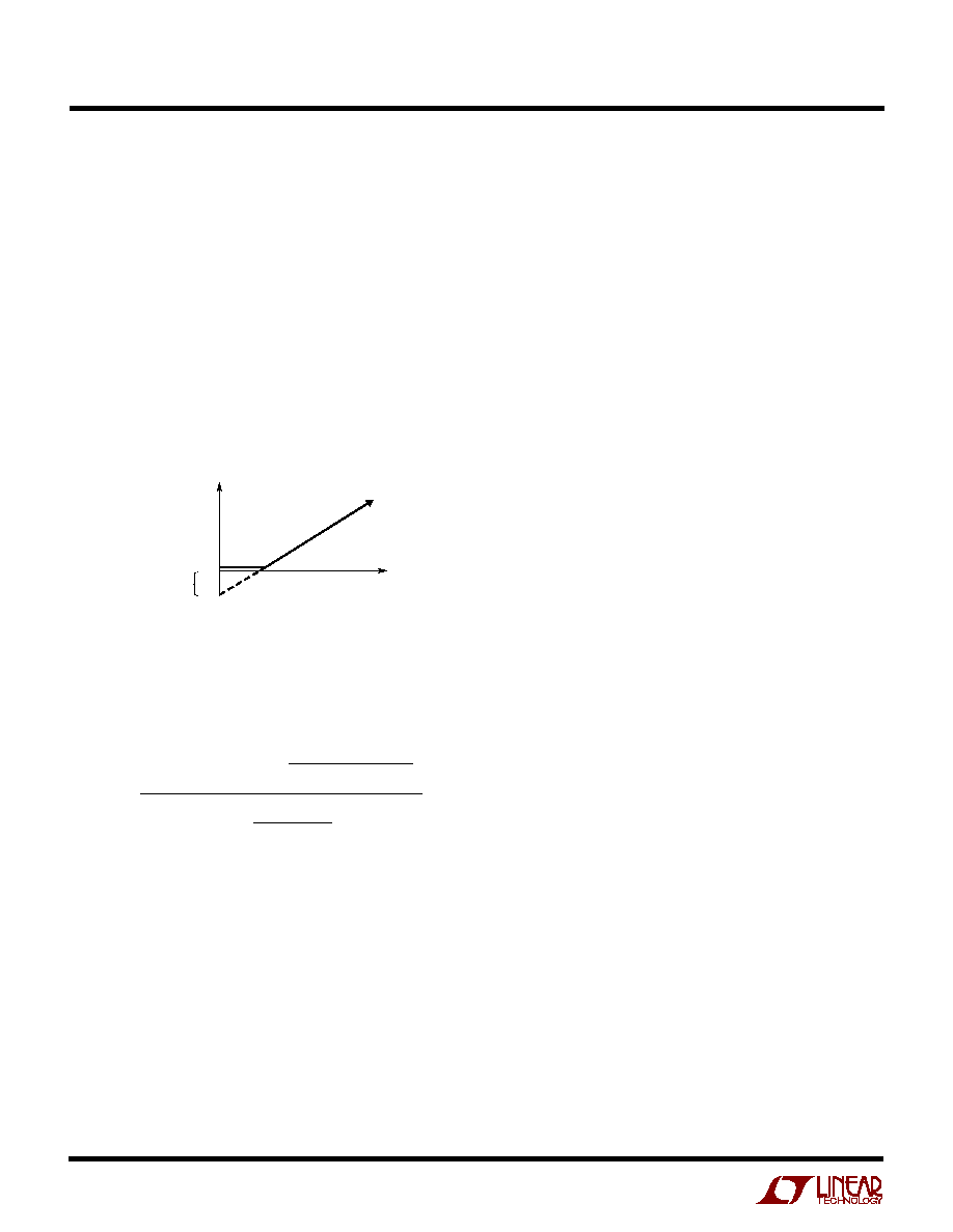
Voltage Offset Error (V
OS
): Normally, DAC offset is the
voltage at the output when the DAC is loaded with all zeros.
The DAC can have a true negative offset, but because the
part is operated from a single supply, the output cannot go
below 0V. If the offset is negative, the output will remain
near 0V resulting in the transfer curve shown in Figure 1.
Therefore, the offset of the part is measured at a code
greater than, "start code":
V
V
Start Code
Start Code V
Start Code
OS
OUT
FS
n
n
=
(
) ≠
(
)(
)
≠
≠
≠
2
1
1
2
1
DAC CODE
1654 F01
OUTPUT
VOLTAGE
NEGATIVE
OFFSET
0V
DEFI ITIO S
U
U

13
LTC1654
1654fa
This circuit shows how to use an LTC1654 and an LT
Æ
1077
to make a wide bipolar output swing 14-bit DAC with an
offset that can be digitally programmed. V
OUTA
, which can
be set by loading the appropriate code for DAC A, sets the
offset. As this value changes, the transfer curve for the
output moves up and down as illustrated in the graph
below.
1
2
3
4
5
6
7
8
16
15
14
13
12
11
10
9
X
1
/X
1/2
B
CLR
SCK
SDI
CS/LD
DGND
SDO
X
1
/X
1/2
A
V
CC
V
OUT B
REFHI B
REFLO B
AGND
REFLO A
REFHI A
V
OUT A
LTC1654
0.1
µ
F
49.9k
1%
5V
1654 TA02
µ
P
100k
1%
49.9k
1%
V
OUT
2 (V
OUTB
≠ V
OUTA
)
15V
≠15V
100k
1%
≠
+
LT1077
V
OUT
0
V
OUTA
0V
V
OUTA
2.5V
V
OUTA
5V
CODE
5
1654 TA03
≠5
≠10
10
16383
A Wide Swing, Bipolar Output 14-Bit DAC with Digitally Controlled Offset
TYPICAL APPLICATIO S
U

14
LTC1654
1654fa
1
2
3
4
5
6
7
8
16
15
14
13
12
11
10
9
X
1
/X
1/2
B
CLR
SCK
SDI
CS/LD
DGND
SDO
X
1
/X
1/2
A
V
CC
V
OUT B
REFHI B
REFLO B
AGND
REFLO A
REFHI A
V
OUT A
LTC1654
0.1
µ
F
2.7V TO 5.5V
OUTPUT B: 0V TO V
CC
OUTPUT A: 0V TO V
CC
1654 TA01
µ
P
Dual 14-Bit Voltage Output DAC
TYPICAL APPLICATIO S
U
15
LTC1654
1654fa
Information furnished by Linear Technology Corporation is believed to be accurate and reliable.
However, no responsibility is assumed for its use. Linear Technology Corporation makes no represen-
tation that the interconnection of its circuits as described herein will not infringe on existing patent rights.
PACKAGE DESCRIPTIO
N
U
GN16 (SSOP) 0502
1
2
3
4
5
6
7
8
.229 ≠ .244
(5.817 ≠ 6.198)
.150 ≠ .157**
(3.810 ≠ 3.988)
16 15 14 13
.189 ≠ .196*
(4.801 ≠ 4.978)
12 11 10 9
.016 ≠ .050
(0.406 ≠ 1.270)
.015
±
.004
(0.38
±
0.10)
◊
45
∞
0
∞
≠ 8
∞
TYP
.007 ≠ .0098
(0.178 ≠ 0.249)
.053 ≠ .068
(1.351 ≠ 1.727)
.008 ≠ .012
(0.203 ≠ 0.305)
.004 ≠ .0098
(0.102 ≠ 0.249)
.0250
(0.635)
BSC
.009
(0.229)
REF
.254 MIN
RECOMMENDED SOLDER PAD LAYOUT
.150 ≠ .165
.0250 TYP
.0165
±
.0015
.045
±
.005
*DIMENSION DOES NOT INCLUDE MOLD FLASH. MOLD FLASH
SHALL NOT EXCEED 0.006" (0.152mm) PER SIDE
**DIMENSION DOES NOT INCLUDE INTERLEAD FLASH. INTERLEAD
FLASH SHALL NOT EXCEED 0.010" (0.254mm) PER SIDE
INCHES
(MILLIMETERS)
NOTE:
1. CONTROLLING DIMENSION: INCHES
2. DIMENSIONS ARE IN
3. DRAWING NOT TO SCALE
GN Package
16-Lead Plastic SSOP (Narrow .150 Inch)
(Reference LTC DWG # 05-08-1641)
16
LTC1654
1654fa
©
LINEAR TECHNOLOGY CORPORATION 2000
Linear Technology Corporation
1630 McCarthy Blvd., Milpitas, CA 95035-7417
(408) 432-1900
q
FAX: (408) 434-0507
q
www.linear.com
LT/TP 1202 1K REV A ∑ PRINTED IN USA
RELATED PARTS
PART NUMBER
DESCRIPTION
COMMENTS
LTC1257
Single 12-Bit V
OUT
DAC, Full Scale: 2.048V, V
CC
: 4.75V to 15.75V,
5V to 15V Single Supply, Complete V
OUT
DAC in
Reference Can Be Overdriven Up to 12V, i.e., FS
MAX
= 12V
SO-8 Package
LTC1446/LTC1446L
Dual 12-Bit V
OUT
DACs in SO-8 Package
LTC1446: V
CC
= 4.5V to 5.5V, V
OUT
= 0V to 4.095V
LTC1446L: V
CC
= 2.7V to 5.5V, V
OUT
= 0V to 2.5V
LTC1448
Dual 12-Bit V
OUT
DAC, V
CC
: 2.7V to 5.5V
Output Swings from GND to REF. REF Input
Can Be Tied to V
CC
LTC1450/LTC1450L
Single 12-Bit V
OUT
DACs with Parallel Interface
LTC1450: V
CC
= 4.5V to 5.5V, V
OUT
= 0V to 4.095V
LTC1450L: V
CC
= 2.7V to 5.5V, V
OUT
= 0V to 2.5V
LTC1451
Single Rail-to-Rail 12-Bit DAC, Full Scale: 4.095V, V
CC
: 4.5V to 5.5V,
5V, Low Power Complete V
OUT
DAC in SO-8 Package
Internal 2.048V Reference Brought Out to Pin
LTC1452
Single Rail-to-Rail 12-Bit V
OUT
Multiplying DAC, V
CC
: 2.7V to 5.5V
Low Power, Multiplying V
OUT
DAC with Rail-to-Rail
Buffer Amplifier in SO-8 Package
LTC1453
Single Rail-to-Rail 12-Bit V
OUT
DAC, Full Scale: 2.5V, V
CC
: 2.7V to 5.5V
3V, Low Power, Complete V
OUT
DAC in SO-8 Package
LTC1454/LTC1454L
Dual 12-Bit V
OUT
DACs in SO-16 Package with Added Functionality
LTC1454: V
CC
= 4.5V to 5.5V, V
OUT
= 0V to 4.095V
LTC1454L: V
CC
= 2.7V to 5.5V, V
OUT
= 0V to 2.5V
LTC1456
Single Rail-to-Rail Output 12-Bit DAC with Clear Pin,
Low Power, Complete V
OUT
DAC in SO-8
Full Scale: 4.095V, V
CC
: 4.5V to 5.5V
Package with Clear Pin
LTC1458/LTC1458L
Quad 12 Bit Rail-to-Rail Output DACs with Added Functionality
LTC1458: V
CC
= 4.5V to 5.5V, V
OUT
= 0V to 4.095V
LTC1458L: V
CC
= 2.7V to 5.5V, V
OUT
= 0V to 2.5V
LTC1658
14-Bit Rail-to-Rail Micropower DAC in MSOP, V
CC
: 2.7V to 5.5V
Output Swings from GND to REF. REF Input
Can Be Tied to V
CC
LTC1659
Single Rail-to-Rail 12-Bit V
OUT
DAC in 8-Pin MSOP, V
CC
: 2.7V to 5.5V
Low Power, Multiplying V
OUT
DAC in MS8 Package.
Output Swings from GND to REF. REF Input Can Be
Tied to V
CC
.
References
LT1460
Micropower Precision Reference
Low Cost, 10ppm Drift
LT1461
Precision Voltage Reference
Ultralow Drift 3ppm/
∞
C, Initial Accuracy: 0.04%
LT1634
Micropower Precision Reference
Low Drift 10ppm/
∞
C, Initial Accuracy: 0.05%