 | ÐлекÑÑоннÑй компоненÑ: LTC1693 | СкаÑаÑÑ:  PDF PDF  ZIP ZIP |
Äîêóìåíòàöèÿ è îïèñàíèÿ www.docs.chipfind.ru
1
LTC1693
High Speed
Single/Dual MOSFET Drivers
s
Dual MOSFET Drivers in SO-8 Package
or Single MOSFET Driver in MSOP Package
s
1G
Electrical Isolation Between the Dual Drivers
Permits High/Low Side Gate Drive
s
1.5A Peak Output Current
s
16ns Rise/Fall Times at V
CC
= 12V, C
L
= 1nF
s
Wide V
CC
Range: 4.5V to 13.2V
s
CMOS Compatible Inputs with Hysteresis,
Input Thresholds are Independent of V
CC
s
Driver Input Can Be Driven Above V
CC
s
Undervoltage Lockout
s
Thermal Shutdown
The LTC
®
1693 family drives power MOSFETs at high
speed. The 1.5A peak output current reduces switching
losses in MOSFETs with high gate capacitance.
The LTC1693-1 contains two noninverting drivers. The
LTC1693-2 contains one noninverting and one inverting
driver. The LTC1693-1 and LTC1693-2 drivers are electri-
cally isolated and independent. The LTC1693-3 is a single
driver with an output polarity select pin.
The LTC1693 has V
CC
independent CMOS input thresh-
olds with 1.2V of typical hysteresis. The LTC1693 can
level-shift the input logic signal up or down to the rail-to-
rail V
CC
drive for the external MOSFET.
The LTC1693 contains an undervoltage lockout circuit and
a thermal shutdown circuit. Both circuits disable the
external N-channel MOSFET gate drive when activated.
The LTC1693-1 and LTC1693-2 come in an 8-lead SO pack-
age. The LTC1693-3 comes in an 8-lead MSOP package.
s
Power Supplies
s
High/Low Side Drivers
s
Motor/Relay Control
s
Line Drivers
s
Charge Pumps
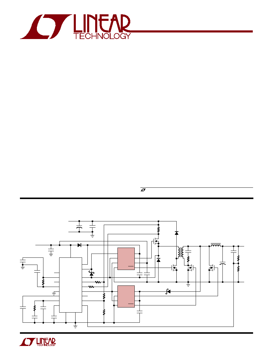
Two Transistor Foward Converter
, LTC and LT are registered trademarks of Linear Technology Corporation.
12V
IN
BOOST
TG
TS
SENSE
+
SENSE
BG
PHASE
RUN/SHDN
V
FB
20
19
18
R6 100
R7 100
11
BAT54
12
16
14
13
R8
301k
1%
R2
5.1
R10
10k
1%
9
8
C15
0.1
µ
F
C14
3300pF
C11
0.1
µ
F
C12
100pF
C7
1
µ
F
C8
1
µ
F
C3
4700pF
25V
C4
0.1
µ
F
L1
1.5
µ
H
T1
13:2
V
OUT
1.5V/15A
RETURN
1693 TA01
C13
1
µ
F
C1: SANYO 63MV330GX
C2: WIMA SMD4036/1.5/63/20/TR
C6: KEMET T510X477M006AS (
×
8)
L1: GOWANDA 50-318
T1: GOWANDA 50-319
C5
1
µ
F
C10
0.1
µ
F
C9
1800pF
5%
NPO
R9
12k
R5
2.49k
1%
15
17
2
1
12V
RETURN
V
IN
48VDC
±
10%
4
3
5
6
7
10
SYNC
5V
REF
SL/ADJ
C
T
I
AVG
SS
V
C
V
REF
PGND
SGND
LT1339
LTC1693CS8-2
D2
MURS120
IN1
GND1
IN2
GND2
8
7
6
5
1
2
3
4
V
CC1
OUT1
V
CC2
OUT2
LTC1693CS8-2
IN1
GND1
IN2
GND2
8
7
6
5
1
2
3
4
V
CC1
OUT1
V
CC2
OUT2
D4
MBRO530T1
D3
MURS120
Q1
MTD20NO6HD
D1
MURS120
C2
1.5
µ
F
63V
C1
330
µ
F
63V
Q3
MTD20NO6HD
Q4
Si4420
R1
0.068
+
Q2
Si4420
×
2
C6
470
µ
F
6.3V
×
8
+
R3
249
1%
R4
1.24k
1%
·
·
DESCRIPTIO
U
FEATURES
APPLICATIO S
U
TYPICAL APPLICATIO
U
2
LTC1693
(Note 1)
Supply Voltage (V
CC
) .............................................. 14V
Inputs (IN, PHASE) ................................... 0.3V to 14V
Driver Output ................................. 0.3V to V
CC
+ 0.3V
GND1 to GND2 (Note 5) .....................................
±
100V
ABSOLUTE
M
AXI
M
U
M
RATINGS
W
W
W
U
Junction Temperature .......................................... 150
°
C
Operating Ambient Temperature Range ....... 0
°
C to 70
°
C
Storage Temperature Range ................. 65
°
C to 150
°
C
Lead Temperature (Soldering, 10 sec).................. 300
°
C
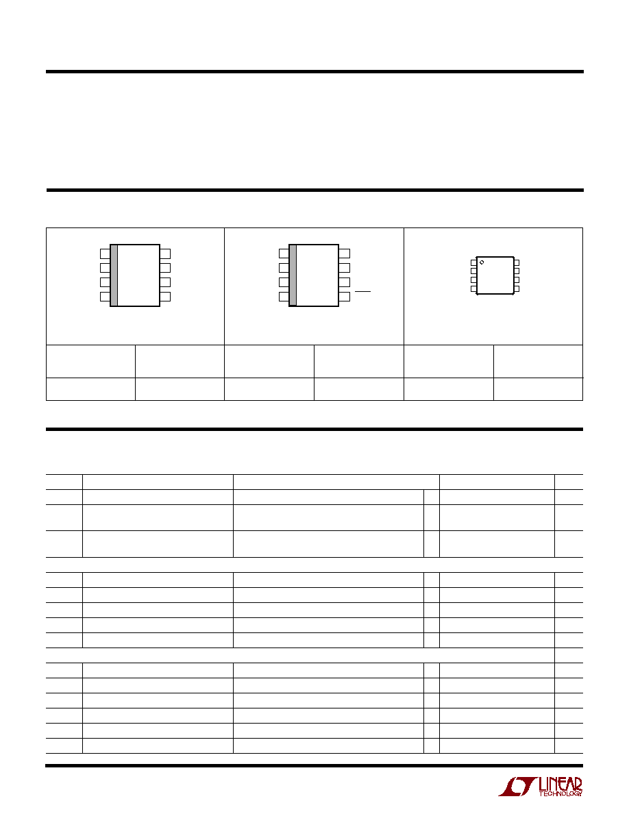
PACKAGE/ORDER I
N
FOR
M
ATIO
N
W
U
U
ORDER PART
NUMBER
S8 PART
MARKING
LTC1693-1CS8
16931
1
2
3
4
8
7
6
5
TOP VIEW
V
CC1
OUT1
V
CC2
OUT2
IN1
GND1
IN2
GND2
S8 PACKAGE
8-LEAD PLASTIC SO
T
JMAX
= 150
°
C,
JA
= 135
°
C/ W
1
2
3
4
8
7
6
5
TOP VIEW
V
CC1
OUT1
V
CC2
OUT2
IN1
GND1
IN2
GND2
S8 PACKAGE
8-LEAD PLASTIC SO
T
JMAX
= 150
°
C,
JA
= 135
°
C/ W
ORDER PART
NUMBER
S8 PART
MARKING
LTC1693-2CS8
16932
1
2
3
4
IN
NC
PHASE
GND
8
7
6
5
V
CC
OUT
NC
NC
TOP VIEW
MS8 PACKAGE
8-LEAD PLASTIC MSOP
T
JMAX
= 150
°
C,
JA
= 200
°
C/ W
ORDER PART
NUMBER
MS8 PART
MARKING
LTC1693-3CMS8
LTEB
Consult factory for Industrial and Military grade parts.
ELECTRICAL CHARACTERISTICS
The
q
denotes specifications which apply over the full operating
temperature range, otherwise specifications are at T
A
= 25
°
C. V
CC
= 12V, unless otherwise noted.
SYMBOL
PARAMETER
CONDITIONS
MIN
TYP
MAX
UNITS
V
CC
Supply Voltage Range
4.5
13.2
V
I
CC
Quiescent Current
LTC1693-1, LTC1693-2, IN1 = IN2 = 0V (Note 2)
q
400
720
1100
µ
A
LTC1693-3, PHASE = 12V, IN = 0V
q
200
360
550
µ
A
I
CC(SW)
Switching Supply Current
LTC1693-1, LTC1693-2, C
OUT
= 4.7nF, f
IN
= 100kHz
q
14.4
20
mA
LTC1693-3, C
OUT
= 4.7nF, f
IN
= 100kHz
q
7.2
10
mA
Input
V
IH
High Input Threshold
q
2.2
2.6
3.1
V
V
IL
Low Input Threshold
q
1.1
1.4
1.7
V
I
IN
Input Pin Bias Current
q
±
0.01
±
10
µ
A
V
PH
PHASE Pin High Input Threshold
(Note 3)
q
4.5
5.5
6.5
V
I
PH
PHASE Pin Pull-Up Current
PHASE = 0V (Note 3)
q
10
20
45
µ
A
Output
V
OH
High Output Voltage
I
OUT
= 10mA
q
11.92
11.97
V
V
OL
Low Output Voltage
I
OUT
= 10mA
q
30
75
mV
R
ONL
Output Pull-Down Resistance
2.85
R
ONH
Output Pull-Up Resistance
3.00
I
PKL
Output Low Peak Current
1.70
A
I
PKH
Output High Peak Current
1.40
A
3
LTC1693
ELECTRICAL CHARACTERISTICS
SYMBOL
PARAMETER
CONDITIONS
MIN
TYP
MAX
UNITS
Switching Timing (Note 4)
t
RISE
Output Rise Time
C
OUT
= 1nF
q
17.5
35
ns
C
OUT
= 4.7nF
q
48.0
85
ns
t
FALL
Output Fall Time
C
OUT
= 1nF
q
16.5
35
ns
C
OUT
= 4.7nF
q
42.0
75
ns
t
PLH
Output Low-High Propagation Delay
C
OUT
= 1nF
q
38.0
70
ns
C
OUT
= 4.7nF
q
40.0
75
ns
t
PHL
Output High-Low Propagation Delay
C
OUT
= 1nF
q
32
70
ns
C
OUT
= 4.7nF
q
35
75
ns
Driver Isolation
R
ISO
GND1-GND2 Isolation Resistance
LTC1693-1, LTC1693-2 GND1-to-GND2 Voltage = 75V
q
0.075
1
G
Note 1: Absolute Maximum Ratings are those values beyond which the life
of a device may be impaired.
Note 2: Supply current is the total current for both drivers.
Note 3: Only the LTC1693-3 has a PHASE pin.
Note 4: All AC timing specificatons are guaranteed by design and are not
production tested.
Note 5: Only applies to the LTC1693-1 and LTC1693-2.
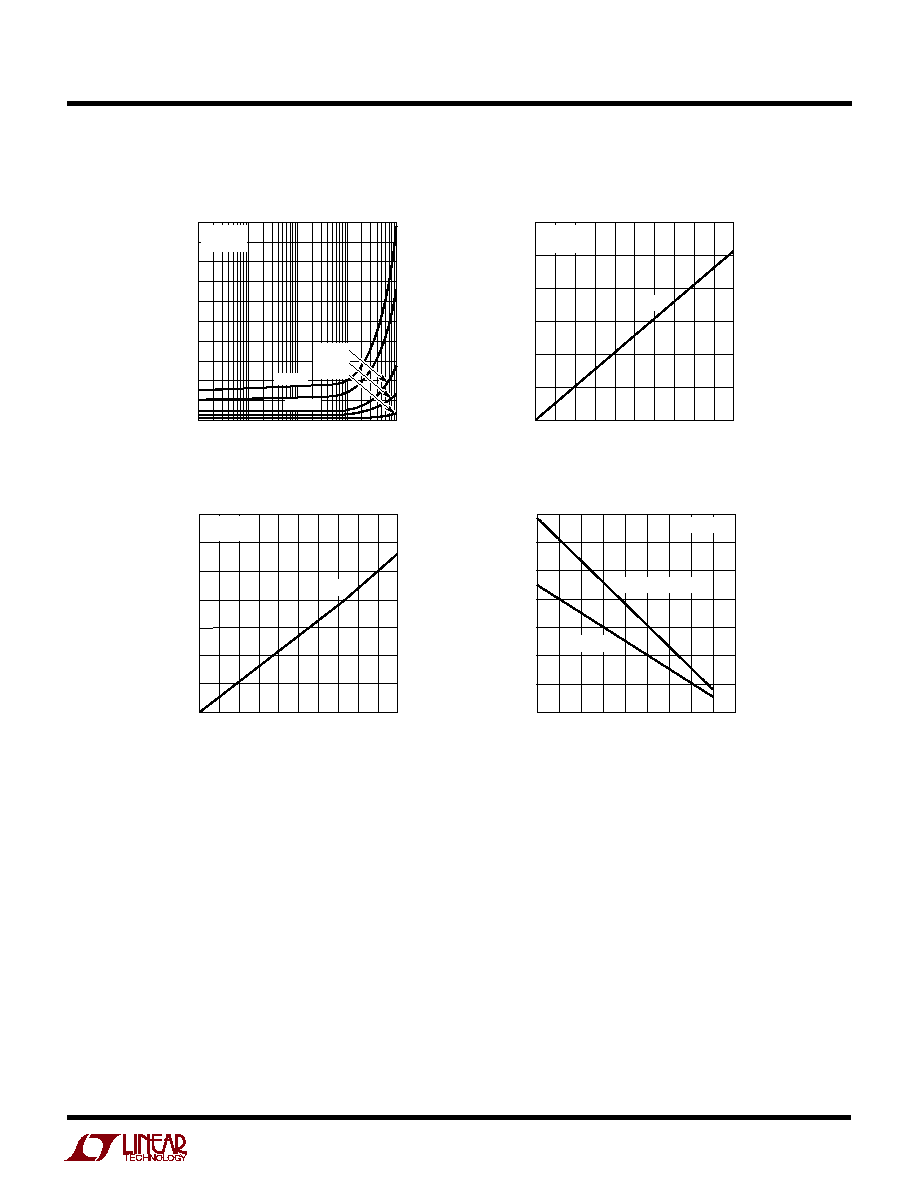
TYPICAL PERFOR A CE CHARACTERISTICS
U
W
IN Threshold Voltage vs V
CC
TEMPERATURE (
°
C)
50
INPUT THRESHOLD HYSTERESIS (V)
1.2
1.3
1.4
25
75
1693 G03
1.1
1.0
25
0
50
100
125
0.9
0.8
V
CC
= 12V
V
IH
-V
IL
IN Threshold Hysteresis
vs Temperature
IN Threshold Voltage
vs Temperature
V
CC
(V)
5
2.00
2.25
2.75
8
10
1693 G01
1.75
1.50
6
7
9
11
12
1.25
1.00
2.50
INPUT THRESHOLD VOLTAGE (V)
V
IH
V
IL
T
A
= 25
°
C
TEMPERATURE (
°
C)
50
INPUT THRESHOLD VOLTAGE (V)
2.75
25
1693 G02
2.00
1.50
25
0
50
1.25
1.00
3.00
2.50
V
IH
V
IL
2.25
1.75
75
100
125
V
CC
= 12V
The
q
denotes specifications which apply over the full operating
temperature range, otherwise specifications are at T
A
= 25
°
C. V
CC
= 12V, unless otherwise noted.
4
LTC1693
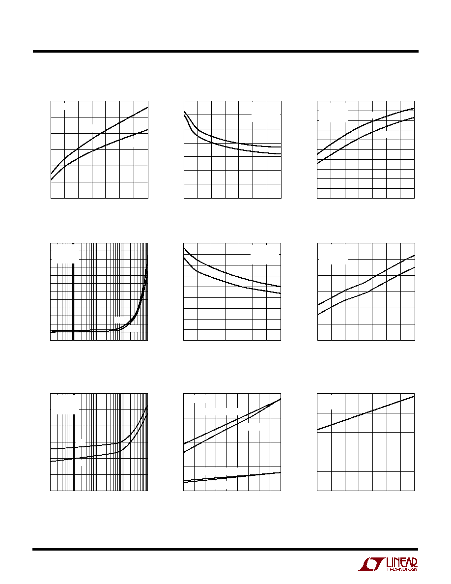
TYPICAL PERFOR A CE CHARACTERISTICS
U
W
PHASE Threshold Voltage vs V
CC
Rise/Fall Time vs V
CC
V
CC
(V)
5
18
20
24
8
10
t
RISE
t
FALL
1693 G05
16
14
6
7
9
11
12
12
10
22
TIME (ns)
T
A
= 25
°
C
C
OUT
= 1nF
f
IN
= 100kHz
Rise/Fall Time vs C
OUT
Propagation Delay vs Temperature
Propagation Delay vs V
CC
Output Saturation Voltage
vs Temperature
Propagation Delay vs C
OUT
TEMPERATURE (
°
C)
55
0
OUTPUT SATURATION VOLTAGE (mV)
50
100
150
200
35 15
5
25
1693 G11
45
65
85 105 125
V
OH
(50mA) wrt V
CC
V
OH
(10mA) wrt V
CC
V
OL
(50mA)
V
OL
(10mA)
V
CC
= 12V
Quiescent Current
vs V
CC
(Single Driver)
V
CC
(V)
5
PHASE THRESHOLD VOLTAGE (V)
4
5
6
8
10
1693 G04
3
2
6
7
9
11
12
1
0
T
A
= 25
°
C
V
PH(H)
V
PH(L)
TEMPERATURE (
°
C)
50
10
TIME (ns)
11
13
14
15
20
17
0
50
75
1693 G06
12
18
19
16
25
25
100
125
V
CC
= 12V
C
OUT
= 1nF
f
IN
= 100kHz
t
RISE
t
FALL
Rise/Fall Time vs Temperature
V
CC
(V)
5
10
TIME (ns)
15
25
30
35
7
55
1693 G08
20
6
8
9
11
10
12
t
PLH
t
PHL
40
45
50
T
A
= 25
°
C
C
OUT
= 1nF
f
IN
= 100kHz
TEMPERATURE (
°
C)
50
TIME (ns)
40
45
50
25
75
1693 G09
35
30
25
0
50
t
PLH
t
PHL
100
125
25
20
V
CC
= 12V
C
OUT
= 1nF
f
IN
= 100kHz
C
OUT
(pF)
30
TIME (ns)
40
50
1
100
1000
10000
1693 G10
20
10
T
A
= 25
°
C
V
CC
= 12V
f
IN
= 100kHz
t
PLH
t
PHL
V
CC
(V)
5
6
100
QUIESCENT CURRENT (
µ
A)
200
350
7
9
10
1693 G12
150
300
250
8
11
12
T
A
= 25
°
C
V
IN
= 0V
C
OUT
(pF)
20
TIME (ns)
40
60
80
100
1
100
1000
10000
1693 G07
0
10
120
T
A
= 25
°
C
V
CC
= 12V
f
IN
= 100kHz
t
RISE
t
FALL
5
LTC1693
TYPICAL PERFOR A CE CHARACTERISTICS
U
W
Switching Supply Current
vs C
OUT
(Single Driver)
V
OH
vs Output Current
C
OUT
(pF)
20
SWITCHING SUPPLY CURRENT (mA)
40
60
50
80
100
10
30
70
90
1
100
1000
10000
1693 G13
0
10
750kHz
500kHz
200kHz
100kHz
25kHz
T
A
= 25
°
C
V
CC
= 12V
OUTPUT CURRENT (mA)
0
0
V
OH
(mV)
50
150
200
250
350
10
50
70
1693 G15
100
300
40
90 100
20 30
60
80
V
OH
T
A
= 25
°
C
V
CC
= 12V
V
OL
vs Output Current
OUTPUT CURRENT (mA)
0
V
OL
(mV)
100
200
300
50
150
250
20
40
60
80
1693 G14
100
10
0
30
50
70
90
V
CC
= 12V
T
A
= 25
°
C
V
OL
AMBIENT TEMPERATURE (
°
C)
55
0
POWER DISSIPATION (mW)
200
600
800
1000
65
85
105
1400
1693 G16
400
35 15
5
25
45
125
1200
T
J
= 125
°
C
LTC1693-3
LTC1693-1/LTC1693-2
Thermal Derating Curves