 | ÐлекÑÑоннÑй компоненÑ: LTC1693-5 | СкаÑаÑÑ:  PDF PDF  ZIP ZIP |
Äîêóìåíòàöèÿ è îïèñàíèÿ www.docs.chipfind.ru
1
LTC1693-5
FEATURES
APPLICATIO S
U
DESCRIPTIO
U
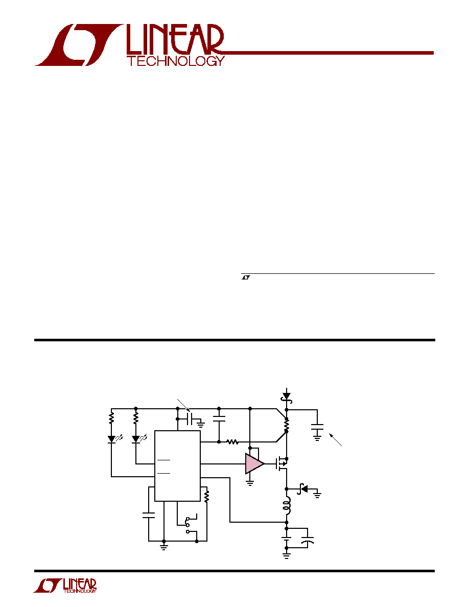
TYPICAL APPLICATIO
U
High Speed Single
P-Channel MOSFET Driver
s
Single MOSFET Driver in MSOP Package
s
1.5A Peak Output Current
s
16ns Rise/Fall Times at V
CC
= 12V, C
L
= 1nF
s
Wide V
CC
Range: 4.5V to 13.2V
s
CMOS Compatible Input with Hysteresis
s
Input Threshold Is Independent of V
CC
s
Driver Input Can Be Driven Above V
CC
s
Undervoltage Lockout
s
Thermal Shutdown
The LTC
®
1693-5 drives power P-channel MOSFETs at
high speed. The 1.5A peak output current reduces switch-
ing losses in MOSFETs with high gate capacitance.
The LTC1693-5 is a single driver with an output polarity
select pin. The MOSFET driver offers V
CC
independent
CMOS input thresholds with 1.2V of typical hysteresis. It
can level-shift the input logic signal up or down to the rail-
to-rail V
CC
drive for the external MOSFET.
The LTC1693-5 contains an undervoltage lockout circuit
and a thermal shutdown circuit that disables the external
P-channel MOSFET gate drive if activated.
The LTC1693-5 comes in an 8-lead MSOP package.
s
Power Supplies
s
High Side Drivers
s
Motor/Relay Control
s
Line Drivers
s
Battery Chargers
High Efficiency 1.5A Li-Ion Battery Charger
, LTC and LT are registered trademarks of Linear Technology Corporation.
SEL
V
CC
4
7
1
LTC1693-5CMS8
4.7
7
3
Si2305DS
MBRS130LT3
MBRS130LT3
V
IN
5V TO 6V
22
µ
F
CDRH6D38-220NC
1-CELL
Li-Ion BATTERY
1693-5 TA01
100
µ
F
8
+
+
DRV
9
SENSE
PROG
1
6
2
18.2k
0.1
µ
F
AVX 0603ZC104KAT1A
USE LOW TEMPERATURE
COEFFICIENT CAPACITOR
CHARGE RATE
1.5A (DEPENDING ON V
IN
AND BATTERY VOLTAGE)
POSITION CAPACITOR CLOSE TO LTC1732
POSITION CAPACITOR
CLOSE TO SENSE RESISTOR
BAT
3
CHRG
TIMER
10
4
ACPR
332
0.082
0.25W
0.47
µ
F
SEL
8
V
CC
LTC1732
5
GND
22
µ
F
CERAMIC
332
1
µ
F
2
LTC1693-5
Note 1: Absolute Maximum Ratings are those values beyond which the life
of a device may be impaired.
Note 2: All AC timing specificatons are guaranteed by design and are not
production tested.
ABSOLUTE
M
AXI
M
U
M
RATINGS
W
W
W
U
Supply Voltage (V
CC
) .............................................. 14V
Inputs (IN, PHASE) ................................... 0.3V to 14V
Driver Output ................................. 0.3V to V
CC
+ 0.3V
Junction Temperature .......................................... 150
°
C
Operating Temperature Range ..................... 0
°
C to 70
°
C
Storage Temperature Range ................. 65
°
C to 150
°
C
Lead Temperature (Soldering, 10 sec).................. 300
°
C
PACKAGE/ORDER I
N
FOR
M
ATIO
N
W
U
U
1
2
3
4
IN
NC
PHASE
GND
8
7
6
5
V
CC
OUT
NC
NC
TOP VIEW
MS8 PACKAGE
8-LEAD PLASTIC MSOP
T
JMAX
= 150
°
C,
JA
= 200
°
C/ W
ORDER PART
NUMBER
MS8 PART
MARKING
LTC1693-5CMS8
LTSG
ELECTRICAL CHARACTERISTICS
The
q
denotes specifications which apply over the full operating
temperature range, otherwise specifications are at T
A
= 25
°
C. V
CC
= 12V, unless otherwise noted.
(Note 1)
Consult factory for parts specified with wider operating temperature ranges.
SYMBOL
PARAMETER
CONDITIONS
MIN
TYP
MAX
UNITS
V
CC
Supply Voltage Range
4.5
13.2
V
I
CC
Quiescent Current
PHASE = 12V, IN = 0V
q
200
360
550
µ
A
I
CC(SW)
Switching Supply Current
C
OUT
= 4.7nF, f
IN
= 100kHz
q
7.2
10
mA
Input
V
IH
High Input Threshold
q
2.2
2.6
3.1
V
V
IL
Low Input Threshold
q
1.1
1.4
1.7
V
I
IN
Input Pin Bias Current
q
±
0.01
±
10
µ
A
V
PH
PHASE Pin High Input Threshold
q
4.5
5.5
6.5
V
I
PH
PHASE Pin Pull-Up Current
PHASE = 0V
q
10
20
45
µ
A
Output
V
OH
High Output Voltage
I
OUT
= 10mA
q
11.92
11.97
V
V
OL
Low Output Voltage
I
OUT
= 10mA
q
30
75
mV
R
ONL
Output Pull-Down Resistance
2.85
R
ONH
Output Pull-Up Resistance
3.00
I
PKL
Output Low Peak Current
1.70
A
I
PKH
Output High Peak Current
1.40
A
Switching Timing (Note 2)
t
RISE
Output Rise Time
C
OUT
= 1nF
q
17.5
35
ns
C
OUT
= 4.7nF
q
48.0
85
ns
t
FALL
Output Fall Time
C
OUT
= 1nF
q
16.5
35
ns
C
OUT
= 4.7nF
q
42.0
75
ns
t
PLH
Output Low-High Propagation Delay
C
OUT
= 1nF
q
38.0
70
ns
C
OUT
= 4.7nF
q
40.0
75
ns
t
PHL
Output High-Low Propagation Delay
C
OUT
= 1nF
q
32
70
ns
C
OUT
= 4.7nF
q
35
75
ns
3
LTC1693-5
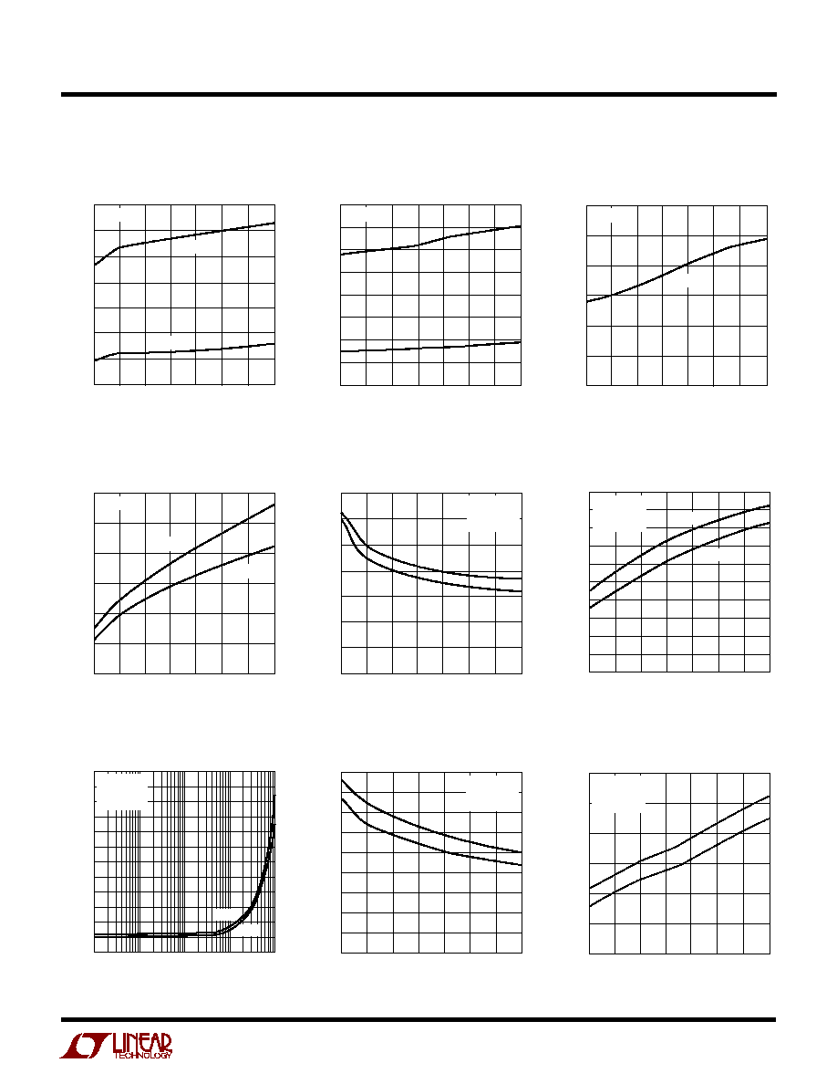
TYPICAL PERFOR A CE CHARACTERISTICS
U
W
IN Threshold Voltage vs V
CC
AMBIENT TEMPERATURE (
°
C)
50
INPUT THRESHOLD HYSTERESIS (V)
1.2
1.3
1.4
25
75
1693-5 G03
1.1
1.0
25
0
50
100
125
0.9
0.8
V
CC
= 12V
V
IH
-V
IL
IN Threshold Hysteresis
vs Ambient Temperature
IN Threshold Voltage
vs Ambient Temperature
V
CC
(V)
5
2.00
2.25
2.75
8
10
1693-5 G01
1.75
1.50
6
7
9
11
12
1.25
1.00
2.50
INPUT THRESHOLD VOLTAGE (V)
V
IH
V
IL
T
A
= 25
°
C
AMBIENT TEMPERATURE (
°
C)
50
INPUT THRESHOLD VOLTAGE (V)
2.75
25
1693-5 G02
2.00
1.50
25
0
50
1.25
1.00
3.00
2.50
V
IH
V
IL
2.25
1.75
75
100
125
V
CC
= 12V
PHASE Threshold Voltage vs V
CC
Rise/Fall Time vs V
CC
V
CC
(V)
5
18
20
24
8
10
t
RISE
t
FALL
1693-5 G05
16
14
6
7
9
11
12
12
10
22
TIME (ns)
T
A
= 25
°
C
C
OUT
= 1nF
f
IN
= 100kHz
Rise/Fall Time vs C
OUT
Propagation Delay vs Ambient
Temperature
Propagation Delay vs V
CC
V
CC
(V)
5
PHASE THRESHOLD VOLTAGE (V)
4
5
6
8
10
1693-5 G04
3
2
6
7
9
11
12
1
0
T
A
= 25
°
C
V
PH(H)
V
PH(L)
AMBIENT TEMPERATURE (
°
C)
50
10
TIME (ns)
11
13
14
15
20
17
0
50
75
1693-5 G06
12
18
19
16
25
25
100
125
V
CC
= 12V
C
OUT
= 1nF
f
IN
= 100kHz
t
RISE
t
FALL
Rise/Fall Time vs Ambient
Temperature
V
CC
(V)
5
10
TIME (ns)
15
25
30
35
7
55
1693-5 G08
20
6
8
9
11
10
12
t
PLH
t
PHL
40
45
50
T
A
= 25
°
C
C
OUT
= 1nF
f
IN
= 100kHz
AMBIENT TEMPERATURE (
°
C)
50
TIME (ns)
40
45
50
25
75
1693-5 G09
35
30
25
0
50
t
PLH
t
PHL
100
125
25
20
V
CC
= 12V
C
OUT
= 1nF
f
IN
= 100kHz
C
OUT
(pF)
20
TIME (ns)
40
60
80
100
1
100
1000
10000
1693-5 G07
0
10
120
T
A
= 25
°
C
V
CC
= 12V
f
IN
= 100kHz
t
RISE
t
FALL
4
LTC1693-5
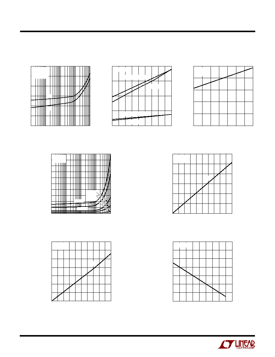
Switching Supply Current vs C
OUT
V
OH
vs Output Current
C
OUT
(pF)
20
SWITCHING SUPPLY CURRENT (mA)
40
60
50
80
100
10
30
70
90
1
100
1000
10000
1693-5 G13
0
10
750kHz
500kHz
200kHz
100kHz
25kHz
T
A
= 25
°
C
V
CC
= 12V
OUTPUT CURRENT (mA)
0
0
V
OH
(mV)
50
150
200
250
350
10
50
70
1693-5 G15
100
300
40
90 100
20 30
60
80
V
OH
T
A
= 25
°
C
V
CC
= 12V
V
OL
vs Output Current
OUTPUT CURRENT (mA)
0
V
OL
(mV)
100
200
300
50
150
250
20
40
60
80
1693-5 G14
100
10
0
30
50
70
90
T
A
= 25
°
C
V
CC
= 12V
V
OL
AMBIENT TEMPERATURE (
°
C)
55
0
POWER DISSIPATION (mW)
200
600
800
1000
65
85
105
1400
1693-5 G16
400
35 15
5
25
45
125
1200
T
J
= 125
°
C
Thermal Derating Curve
TYPICAL PERFOR A CE CHARACTERISTICS
U
W
Output Saturation Voltage
vs Temperature
Propagation Delay vs C
OUT
TEMPERATURE (
°
C)
55
0
OUTPUT SATURATION VOLTAGE (mV)
50
100
150
200
35 15
5
25
1693-5 G11
45
65
85 105 125
V
OH
(50mA) wrt V
CC
V
OH
(10mA) wrt V
CC
V
OL
(50mA)
V
OL
(10mA)
V
CC
= 12V
Quiescent Current vs V
CC
C
OUT
(pF)
30
TIME (ns)
40
50
1
100
1000
10000
1693-5 G10
20
10
T
A
= 25
°
C
V
CC
= 12V
f
IN
= 100kHz
t
PLH
t
PHL
V
CC
(V)
5
6
100
QUIESCENT CURRENT (
µ
A)
200
350
7
9
10
1693-5 G12
150
300
250
8
11
12
T
A
= 25
°
C
V
IN
= 0V
5
LTC1693-5
PI
N
FU
N
CTIO
N
S
U
U
U
IN (Pin 1): Driver Input. The input has V
CC
independent
thresholds with hysteresis to improve noise immunity.
NC (Pins 2, 5, 6): No Connect.
PHASE (Pin 3): Output Polarity Select. Connect this pin to
V
CC
or leave it floating for noninverting operation. Ground
this pin for inverting operation. The typical PHASE pin
input current when pulled low is 20
µ
A.
GND (Pin 4): Driver Ground. Connect to a low impedance
ground. The V
CC
bypass capacitor should connect directly
to this pin.
OUT (Pin 7): Driver Output.
V
CC
(Pin 8): Power Supply Input. The source of the exter-
nal P-MOSFET should also connect directly to this pin.
This minimizes the AC current path and improves signal
integrity.
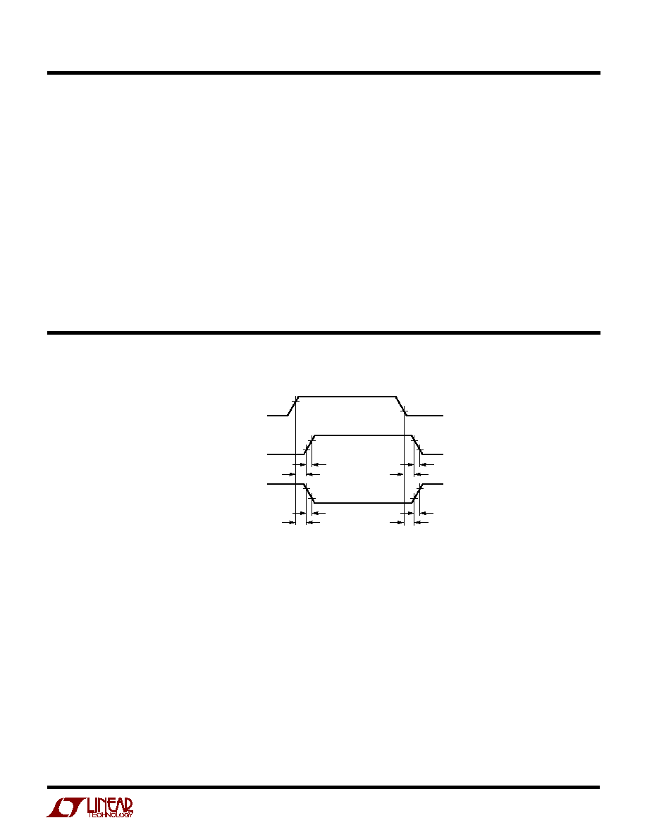
TI I G DIAGRA
U
W
W
V
IH
90%
10%
90%
10%
t
r
t
f
INPUT
NONINVERTING
OUTPUT OPERATION
INVERTING
OUTPUT OPERATION
INPUT RISE/FALL TIME < 10ns
V
IL
t
f
t
PLH
t
PHL
t
PLH
1693-5 TD
t
r
t
PHL