 | –≠–Ľ–Ķ–ļ—ā—Ä–ĺ–Ĺ–Ĺ—č–Ļ –ļ–ĺ–ľ–Ņ–ĺ–Ĺ–Ķ–Ĺ—ā: LTC1702 | –°–ļ–į—á–į—ā—Ć:  PDF PDF  ZIP ZIP |
1
LTC1702
Dual 550kHz Synchronous
2-Phase Switching Regulator Controller
The LTC
ģ
1702 is a dual switching regulator controller opti-
mized for high efficiency with low input voltages. It includes
two complete, on-chip, independent switching regulator
controllers each designed to drive a pair of external N-channel
MOSFET devices in a voltage mode feedback, synchronous
buck configuration. The LTC1702 uses a constant-frequency,
true PWM design switching at 550kHz, minimizing external
component size and cost and maximizing load transient
performance. The synchronous buck architecture automati-
cally shifts to discontinuous and then to Burst Mode
TM
operation as the output load decreases, ensuring maximum
efficiency over a wide range of load currents.
The LTC1702 features an onboard reference trimmed to
0.5% and can provide better than 1% regulation at the
converter outputs. Open-drain logic outputs indicate whether
either output has risen to within 5% of the final output voltage
and an optional latching FAULT mode protects the load if the
output rises 15% above the intended voltage. Each channel
can be enabled independently; with both channels disabled,
the LTC1702 shuts down and supply current drops below
100
Ķ
A.
s
Two Independent Controllers in One Package
s
Two Sides Run Out-of-Phase to Minimize C
IN
s
All N-Channel External MOSFET Architecture
s
No External Current Sense Resistors
s
Excellent Output Regulation: 1% Total Output
Accuracy
s
550kHz Switching Frequency Minimizes External
Component Size
s
1A to 25A Output Current per Channel
s
High Efficiency over Wide Load Current Range
s
Quiescent Current Drops Below 100
Ķ
A in Shutdown
s
Small 24-Pin Narrow SSOP Package
, LTC and LT are registered trademarks of Linear Technology Corporation.
Burst Mode is a trademark of Linear Technology Corporation.
s
Microprocessor Core and I/O Supplies
s
Multiple Logic Supply Generator
s
Distributed Power Applications
s
High Efficiency Power Conversion
Dual Output High Power 3.3V/2.5V Logic Supply
DESCRIPTIO
U
FEATURES
APPLICATIO S
U
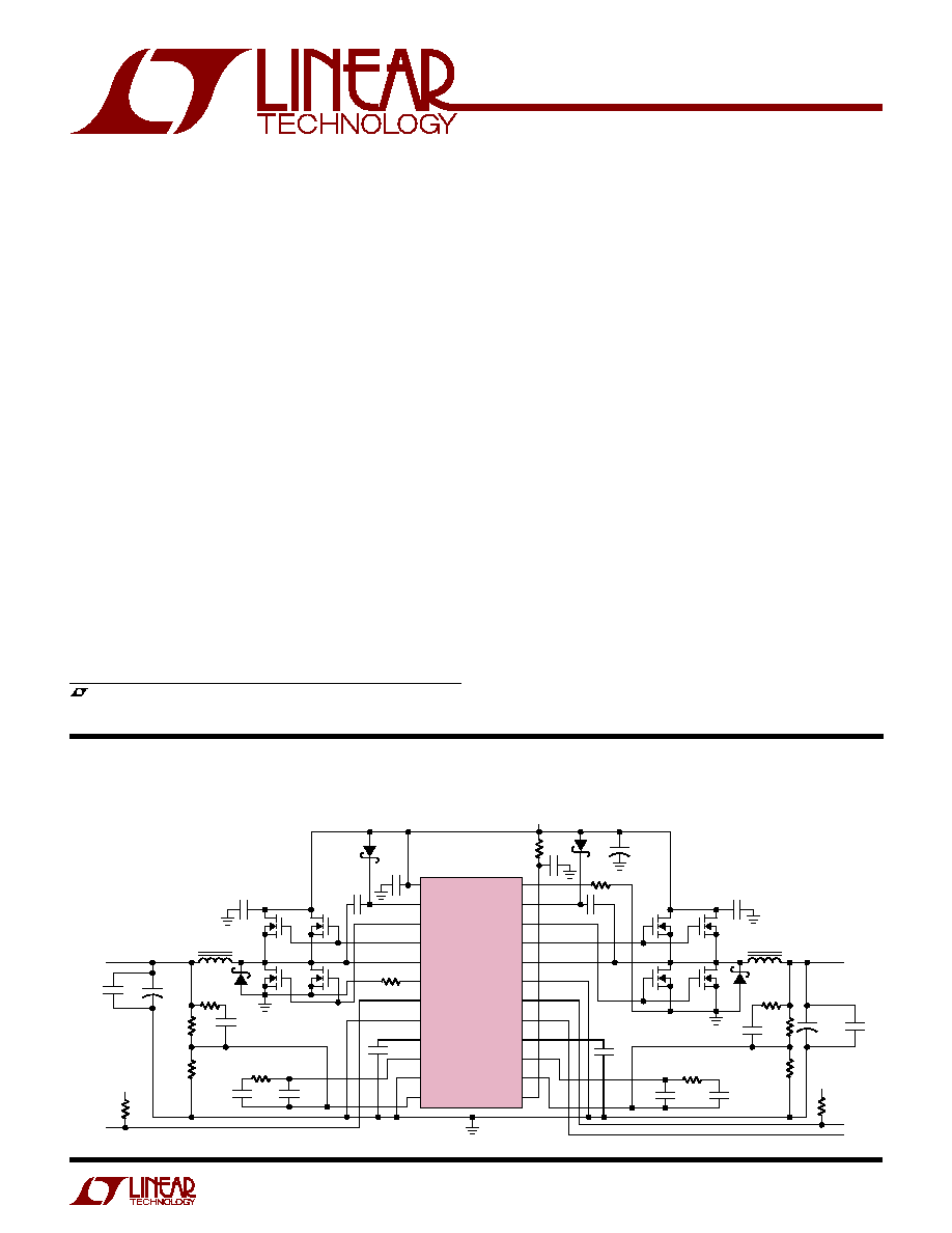
TYPICAL APPLICATIO
U
LTC1702
PV
CC
BOOST1
BG1
TG1
SW1
I
MAX1
PGOOD1
FCB
RUN/SS
COMP1
SGND
FB1
I
MAX2
BOOST2
BG2
TG2
SW2
PGND
PGOOD2
FAULT
RUN/SS2
COMP2
FB2
V
CC
1
2
3
4
5
6
7
8
9
10
11
12
24
23
22
21
20
19
18
17
16
15
14
13
1
Ķ
F
10
1
Ķ
F
1
Ķ
F
27k
27k
1.6k
68k
1702 TA01
V
IN
1.2k
10k
1%
C
OUT1
180
Ķ
F
◊
4
820pF
27pF
680pF
47k
1
Ķ
F
V
OUT1
2.5V
AT 15A
1
Ķ
F
4.75k
1%
Q2
Q1
Q4
Q3
D3
D2
C
OUT1
, C
OUT2
: PANASONIC EEFUE0G181R
C
IN
: KEMET TS10X337M010AS
D1, D2: MOTOROLA MBR0520LT1
D3, D4: MOTOROLA MBRS320T3
L1, L2: SUMIDA CEP125-1R0
Q1 TO Q8: FAIRCHILD FDS6670A
D1
PWRGD1
L1
1
Ķ
H
+
10
Ķ
F
10
Ķ
F
1
Ķ
F
V
IN
= 5V
Ī
10%
1
Ķ
F
C
IN
330
Ķ
F
◊
3
+
Q7
Q5
Q8
Q6
D4
680pF
27pF
3300pF
15.8k
1%
4.99k
1%
10k
L2
1
Ķ
H
C
OUT2
180
Ķ
F
◊
4
1
Ķ
F
V
OUT2
3.3V/15A
PWRGD2
FAULT
+
V
IN
10k
2
LTC1702
ABSOLUTE
M
AXI
M
U
M
RATINGS
W
W
W
U
(Note 1)
Supply Voltage
V
CC ...........................................................................................
7V
BOOST
n ............................................................... 15V
BOOST
n ≠ SWn .................................................... 7V
Input Voltage
SW
n .......................................................... ≠ 1V to 8V
All Other Inputs ......................... ≠ 0.3V to V
CC
+ 0.3V
Peak Output Current < 10
Ķ
s
TG
n, BGn ............................................................... 5A
Operating Temperature Range
LTC1702C ............................................... 0
į
C to 70
į
C
LTC1702I ........................................... ≠ 40
į
C to 85
į
C
Storage Temperature Range ................. ≠ 65
į
C to 150
į
C
Lead Temperature (Soldering, 10 sec).................. 300
į
C
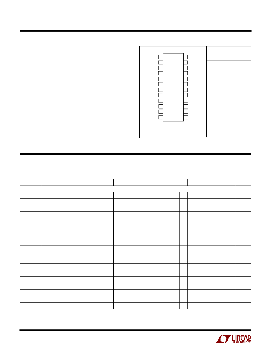
PACKAGE/ORDER I
N
FOR
M
ATIO
N
W
U
U
ORDER PART
NUMBER
1
2
3
4
5
6
7
8
9
10
11
12
TOP VIEW
GN PACKAGE
24-LEAD NARROW PLASTIC SSOP
24
23
22
21
20
19
18
17
16
15
14
13
PV
CC
BOOST1
BG1
TG1
SW1
I
MAX1
PGOOD1
FCB
RUN/SS1
COMP1
SGND
FB1
I
MAX2
BOOST2
BG2
TG2
SW2
PGND
PGOOD2
FAULT
RUN/SS2
COMP2
FB2
V
CC
T
JMAX
= 125
į
C,
JA
= 100
į
C/ W
LTC1702CGN
LTC1702IGN
Consult factory for Military grade parts.
ELECTRICAL CHARACTERISTICS
SYMBOL
PARAMETER
CONDITIONS
MIN
TYP
MAX
UNITS
Main Control Loop
V
CC
V
CC
Supply Voltage
q
3
7
V
PV
CC
PV
CC
Supply Voltage
(Note 2)
q
3
7
V
BV
CC
BOOST Pin Voltage
V
BOOST
≠ V
SW
(Note 2)
q
2.7
7
V
I
CC
V
CC
Supply Current
Test Circuit 1, C
L
= 0pF
q
2.2
8
mA
RUN/SS1 = RUN/SS2 = 0V (Note 5)
q
30
100
Ķ
A
IPV
CC
PV
CC
Supply Current
Test Circuit 1, C
L
= 0pF (Note 4)
q
2.2
6
mA
RUN/SS1 = RUN/SS2 = 0V (Note 5)
q
6
100
Ķ
A
I
BOOST
BOOST Pin Current
Test Circuit 1, C
L
= 0pF (Note 4)
q
1.3
3
mA
RUN/SS1 = RUN/SS2 = 0V
q
0.1
10
Ķ
A
V
FB
Feedback Voltage
Test Circuit 1, C
L
= 0pF, LTC1702C
q
0.792
0.800
0.808
V
Test Circuit 1, C
L
= 0pF, LTC1702I
q
0.790
0.800
0.810
V
V
FB
Feedback Voltage Line Regulation
V
CC
= 3V to 7V
q
Ī
0.005
Ī
0.05
%/V
I
FB
Feedback Current
q
Ī
0.001
Ī
1
Ķ
A
V
OUT
Output Voltage Load Regulation
(Note 6)
q
0.1
Ī
0.2
%
V
FCB
FCB Threshold
q
0.75
0.8
0.85
V
V
FCB
FCB Feedback Hysteresis
20
mV
I
FCB
FCB Pin Current
q
Ī
0.001
Ī
1
Ķ
A
V
RUN
RUN/SS Pin RUN Threshold
q
0.45
0.55
0.65
V
I
SS
Soft-Start Source Current
RUN/SS
n = 0V
≠ 2
≠ 3.5
≠ 6
Ķ
A
The
q
denotes specifications which apply over the full operating temperature range, otherwise specifications are TA = 25
į
C.
V
CC
= 5V unless otherwise specified. (Note 3)
3
LTC1702
ELECTRICAL CHARACTERISTICS
Note 1: Absolute Maximum Ratings are those values beyond which the life
of a device may be impaired.
Note 2: PV
CC
and BV
CC
(V
BOOST
≠ V
SW
) must be greater than V
GS(ON)
of
the external MOSFETs used to ensure proper operation.
Note 3: All currents into device pins are positive; all currents out of device
pins are negative. All voltages are referenced to ground unless otherwise
specified.
Note 4: Supply current in normal operation is dominated by the current
needed to charge and discharge the external MOSFET gates. This current
will vary with supply voltage and the external MOSFETs used.
Note 5: Supply current in shutdown is dominated by external MOSFET
leakage and may be significantly higher than the quiescent current drawn
by the LTC1702, especially at elevated temperature.
Note 6: This parameter is guaranteed by correlation and is not tested
directly.
Note 7: Rise and fall times are measured using 10% and 90% levels. Delay
and nonoverlap times are measured using 50% levels.
The
q
denotes specifications which apply over the full operating temperature range, otherwise specifications are TA = 25
į
C.
V
CC
= 5V unless otherwise specified. (Note 3)
SYMBOL
PARAMETER
CONDITIONS
MIN
TYP
MAX
UNITS
Switching Characteristics
f
OSC
Oscillator Frequency
Test Circuit 1, C
L
= 0pF
q
475
550
750
kHz
OSC2
Converter 2 Oscillator Phase
Relative to Converter 1 (Note 6)
180
DEG
DC
MIN1
Minimum Duty Cycle
V
FB
< V
MAX
q
7
10
%
DC
MIN2
Minimum Duty Cycle
V
FB
> V
MAX
q
0
%
DC
MAX
Maximum Duty Cycle
q
87
90
93
%
t
NOV
Driver Nonoverlap
Test Circuit 1, C
L
= 2000pF (Note 7)
q
40
100
ns
t
r
, t
f
Driver Rise/Fall Time
Test Circuit 1, C
L
= 2000pF (Note 7)
q
12
80
ns
Feedback Amplifier
A
VFB
FB DC Gain
q
74
85
dB
GBW
FB Gain Bandwidth
25
MHz
I
ERR
FB Sink/Source Current
q
Ī
3
Ī
10
mA
V
MIN
MIN Comparator Threshold
q
760
785
mV
V
MAX
MAX Comparator Threshold
q
815
840
mV
Current Limit Loop
A
VILIM
I
LIM
Gain
40
dB
I
IMAX
I
MAX
Source Current
I
MAX
= 0V, LTC1702C
q
≠ 7
≠10
≠13
Ķ
A
I
MAX
= 0V, LTC1702I
q
≠ 7
≠10
≠14
Ķ
A
Status Outputs
V
PGOOD
PGOOD Trip Point
V
FB
Relative to Regulated V
OUT
q
≠ 10
≠ 5
≠ 2
%
V
OLPG
PGOOD Output Low Voltage
PGOOD = 1mA
q
0.03
0.1
V
I
PGOOD
PGOOD Output Leakage
q
Ī
0.1
Ī
1
Ķ
A
t
PGOOD
PGOOD Delay Time
V
FB
< V
PGOOD
to PGOOD (Note 7)
100
Ķ
s
V
FAULT
FAULT Trip Point
V
FB
Relative to Regulated V
OUT
q
+ 10
+ 15
+ 20
%
V
OLF
FAULT Output Low Voltage
I
FAULT
= 1mA
q
0.03
0.1
V
I
FAULT
FAULT Output Current
V
FAULT
= 0V
≠ 10
Ķ
A
t
FAULT
FAULT Delay Time
V
FB
> V
FAULT
to FAULT (Note 7)
25
Ķ
s
4
LTC1702
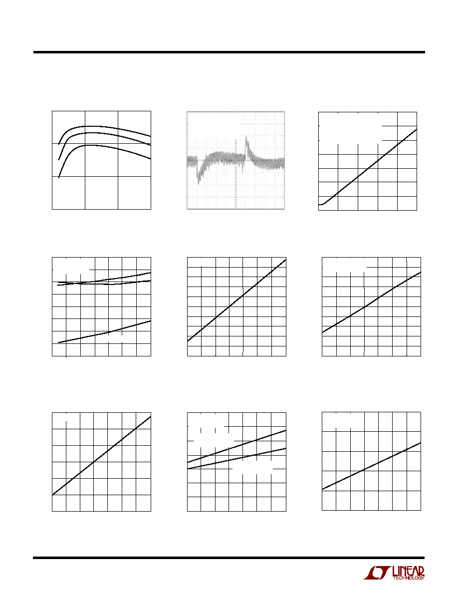
TYPICAL PERFOR A CE CHARACTERISTICS
U
W
Efficiency vs Load Current
TEMPERATURE (
į
C)
≠ 50
SUPPLY CURRENT (mA)
2.4
PV
CC
V
CC
25
1702 G04
1.8
1.4
≠ 25
0
50
1.2
1.0
2.6
2.2
2.0
1.6
75
100
125
BOOST1, BOOST2
TEST CIRCUIT 1
C
L
= 0pF
Transient Response
TEMPERATURE (
į
C)
≠50
≠2.5
NORMALIZED FREQUENCY (%)
≠2.0
≠1.0
≠0.5
0
2.5
1.0
0
50
75
1702 G05
≠1.5
1.5
2.0
0.5
≠25
25
100
125
V
CC
= 5V
TEMPERATURE (
į
C)
≠50
0.4
R
ON
(
)
0.5
0.7
0.8
0.9
1.4
1.1
0
50
75
1702 G06
0.6
1.2
1.3
1.0
≠25
25
100
125
V
PVCC
= 5V
V
BOOST
≠ V
SW
= 5V
MOSFET Driver Supply Current
vs Gate Capacitance
Supply Current vs Temperature
Normalized Frequency
vs Temperature
Driver R
ON
vs Temperature
RUN/SS Source Current
vs Temperature
TEMPERATURE (
į
C)
≠50
SOURCE CURRENT (
Ķ
A)
4.0
4.5
5.0
25
75
1702 G07
3.5
3.0
≠25
0
50
100
125
2.5
2.0
V
CC
= 5V
Nonoverlap Time vs Temperature
Driver Rise/Fall vs Temperature
LOAD CURRENT (A)
0
70
EFFICIENCY (%)
80
90
100
5
10
1702 G01
15
V
IN
= 5V
V
OUT
= 3.3V
V
OUT
= 2.5V
V
OUT
= 1.6V
V
IN
= 5V
V
OUT
= 1.8V
I
LOAD
= 0A-10A-0A
Ī
2.2% MAX DEVIATION
1702 G02
GATE CAPACITANCE (pF)
0
25
30
35
6000
8000
1702 G03
20
15
2000
4000
10000
10
5
0
DRIVER SUPPLY CURRENT (mA)
TEST CIRCUIT 1
ONE DRIVER LOADED
MULTIPLY BY # OF ACTIVE
DRIVERS TO OBTAIN TOTAL
DRIVER SUPPLY CURRENT
TEMPERATURE (
į
C)
≠50
40
50
70
25
75
1702 G08
30
20
≠25
0
50
100
125
10
0
60
NONOVERLAP (ns)
TEST CIRCUIT 1
C
L
= 2000pF
BG FALLING EDGE
TG RISING EDGE
TG FALLING EDGE
BG RISING EDGE
TEMPERATURE (
į
C)
≠50
≠25
12
RISE/FALL TIME (ns)
12
15
0
50
75
1702 G09
11
14
13
25
100
125
TEST CIRCUIT 1
C
L
= 2000pF
20mV/
DIV
10
Ķ
s/DIV

5
LTC1702
PI
N
FU
N
CTIO
N
S
U
U
U
FB1
falls 5% below its programmed value. When RUN/SS1
is low (side 1 shut down), PGOOD1 will go high.
FCB (Pin 8): Force Continuous Bar. The FCB pin forces
both converters to maintain continuous synchronous
operation regardless of load when the voltage at FCB
drops below 0.8V. FCB is normally tied to V
CC
. To force
continuous operation, tie FCB to SGND. FCB can also be
connected to a feedback resistor divider from a secondary
winding on one converter's inductor to generate a third
regulated output voltage. Do not leave FCB floating.
RUN/SS1 (Pin 9): Controller 1 Run/Soft-start. Pulling
RUN/SS1 to SGND will disable controller 1 and turn off
both of its external MOSFET switches. Pulling both
RUN/SS pins down will shut down the entire LTC1702,
dropping the quiescent supply current below 100
Ķ
A. A
capacitor from RUN/SS1 to SGND will control the turn-on
time and rate of rise of the controller 1 output voltage at
power-up. An internal 3.5
Ķ
A current source pull-up at
RUN/SS1 pin sets the turn-on time at approximately
500ms/
Ķ
F.
COMP1 (Pin 10): Controller 1 Loop Compensation. The
COMP1 pin is connected directly to the output of the first
controller's error amplifier and the input to the PWM
comparator. An RC network is used at the COMP1 pin to
compensate the feedback loop for optimum transient
response.
SGND (Pin 11): Signal Ground. All internal low power
circuitry returns to the SGND pin. Connect to a low
impedance ground, separated from the PGND node. All
feedback, compensation and soft-start connections should
return to SGND. SGND and PGND should connect only at
a single point, near the PGND pin and the negative plate of
the C
IN
bypass capacitor.
FB1 (Pin 12): Controller 1 Feedback Input. FB1 should be
connected through a resistor network to V
OUT1
to set the
output voltage. The loop compensation network for con-
troller 1 also connects to FB1.
V
CC
(Pin 13): Power Supply Input. All internal circuits
except the output drivers are powered from this pin. V
CC
should be connected to a low noise power supply voltage
between 3V and 7V and should be bypassed to SGND with
at least a 1
Ķ
F capacitor in close proximity to the LTC1702.
PV
CC
(Pin 1): Driver Power Supply Input. PV
CC
provides
power to the two BG
n output drivers. PV
CC
must be
connected to a voltage high enough to fully turn on the
external MOSFETs QB1 and QB2. PV
CC
should generally
be connected directly to V
IN
. PV
CC
requires at least a 1
Ķ
F
bypass capacitor directly to PGND.
BOOST1 (Pin 2): Controller 1 Top Gate Driver Supply. The
BOOST1 pin supplies power to the floating TG1 driver.
BOOST1 should be bypassed to SW1 with a 1
Ķ
F capacitor.
An additional Schottky diode from V
IN
to BOOST1 pin will
create a complete floating charge-pumped supply at
BOOST1. No other external supplies are required.
BG1 (Pin 3): Controller 1 Bottom Gate Drive. The BG1 pin
drives the gate of the bottom N-channel synchronous
switch MOSFET, QB1. BG1 is designed to drive up to
10,000pF of gate capacitance directly. If RUN/SS1 goes
low, BG1 will go low, turning off QB1. If FAULT mode is
tripped, BG1 will go high and stay high, keeping QB1 on
until the power is cycled.
TG1 (Pin 4): Controller 1 Top Gate Drive. The TG1 pin
drives the gate of the top N-channel MOSFET, QT1. The
TG1 driver draws power from the BOOST1 pin and returns
to the SW1 pin, providing true floating drive to QT1. TG1
is designed to drive up to 10,000pF of gate capacitance
directly. In shutdown or fault modes, TG1 will go low.
SW1 (Pin 5): Controller 1 Switching Node. SW1 should be
connected to the switching node of converter 1. The TG1
driver ground returns to SW1, providing floating gate
drive to the top N-channel MOSFET switch, QT1. The
voltage at SW1 is compared to I
MAX1
by the current limit
comparator while the bottom MOSFET, QB1, is on.
I
MAX1
(Pin 6): Controller 1 Current Limit Set. The I
MAX1
pin sets the current limit comparator threshold for
controller 1. If the voltage drop across the bottom MOSFET,
QB1, exceeds the magnitude of the voltage at I
MAX1
,
controller 1 will go into current limit. The I
MAX1
pin has an
internal 10
Ķ
A current source pull-up, allowing the current
threshold to be set with a single external resistor to PGND.
See the Current Limit Programming section for more
information on choosing R
IMAX
.
PGOOD1 (Pin 7): Controller 1 Power Good. PGOOD1 is an
open-drain logic output. PGOOD1 will pull low whenever
6
LTC1702
FB2 (Pin 14): Controller 2 Feedback Input. See FB1.
COMP2 (Pin 15): Controller 2 Loop Compensation. See
COMP1.
RUN/SS2 (Pin 16): Controller 2 Run/Soft-start. See RUN/
SS1.
FAULT (Pin 17): Output Overvoltage Fault (Latched). The
FAULT pin is an open-drain output with an internal 10
Ķ
A
pull-up. If either regulated output voltage rises more than
15% above its programmed value for more than 25
Ķ
s, the
FAULT output will go high and the entire LTC1702 will be
disabled. When FAULT is high, both BG pins will go high,
turning on the bottom MOSFET switches and pulling down
the high output voltage. The LTC1702 will remain latched
in this state until the power is cycled. When FAULT mode
is active, the FAULT pin will be pulled up with an internal
10
Ķ
A current source. Tying FAULT directly to PGND will
PI
N
FU
N
CTIO
N
S
U
U
U
disable latched FAULT mode and will allow the LTC1702 to
resume normal operation when the overvoltage fault is
removed.
PGOOD2 (Pin 18): Controller 2 Power Good. See PGOOD1.
PGND (Pin 19): Power Ground. The BG
n drivers return to
this pin. Connect PGND to a high current ground node in
close proximity to the sources of external MOSFETs, QB1
and QB2, and the V
IN
and V
OUT
bypass capacitors.
SW2 (Pin 20): Controller 2 Switching Node. See SW1.
TG2 (Pin 21): Controller 2 Top Gate Drive. See TG1.
BG2 (Pin 22): Controller 2 Bottom Gate Drive. See BG1.
BOOST2 (Pin 23): Controller 2 Top Gate Driver Supply.
See BOOST1.
I
MAX2
(Pin 24): Controller 2 Current Limit Set. See I
MAX1
.
BLOCK DIAGRA
M
W
BURST
LOGIC
SOFT
START
90% DUTY CYCLE
RUN/SS1,2
COMP1,2
10
Ķ
A
3.5
Ķ
A
1V
P-P
550mV
800mV
760mV
840mV
I
MAX1,2
DRIVE
LOGIC
100
Ķ
s
DELAY
OSC
550kHz
+
≠
I
LIM
FB
MIN
MAX
920mV
FLT
DIS
FCB
FB1,2
1702 BD
BOOST1,2
TG1,2
FROM
OTHER
CONTROLLER
SHUTDOWN TO
THIS CONTROLLER
SHUTDOWN TO
ENTIRE CHIP
FAULT
PV
CC
25
Ķ
s
DELAY
FROM
OTHER
CONTROLLER
V
CC
SW1,2
BG1,2
PGND
SGND
PGOOD1,2
7
LTC1702
TEST CIRCUIT
Test Circuit 1
controllers allow, improving stability and maximizing tran-
sient response. The 800mV internal reference allows
regulated output voltages as low as 800mV without exter-
nal level shifting amplifiers.
The LTC1702's synchronous switching logic transitions
automatically into Burst Mode operation, maximizing effi-
ciency with light loads. Onboard power-good and over-
voltage (OV) fault flags indicate when the output is in
regulation or an OV fault has occurred. The OV flag can be
set to latch the device off when an OV fault has occurred,
or to automatically resume operation when the fault is
removed.
The LTC1702 takes a low input voltage and generates two
lower output voltages at very high currents. Its strengths
are small size, unmatched regulation and transient
response and high efficiency. This combination makes it
ideal for providing multiple low voltage logic supplies to
microprocessors or high density ASICs in systems using
a "2-step" regulation architecture, used in portable and
advanced desktop computers.
OVERVIEW
The LTC1702 is a dual, step-down (buck), voltage mode
feedback switching regulator controller. It is designed to
be used in a synchronous switching architecture with two
external N-channel MOSFETs per channel. It is intended to
operate from a low voltage input supply (7V maximum)
and provide a high power, high efficiency, precisely regu-
lated output voltage. Several features make it particularly
suited for microprocessor supply regulation. Output regu-
lation is extremely tight, with DC line and load regulation
and initial accuracy better than 1%, and total regulation
including transient response inside of 3% with a properly
designed circuit. The 550kHz switching frequency allows
the use of physically small, low value external components
without compromising performance.
The LTC1702's internal feedback amplifier is a 25MHz
gain-bandwidth op amp, allowing the use of complex
multipole/zero compensation networks. This allows the
feedback loop to maintain acceptable phase margin at
higher frequencies than traditional switching regulator
APPLICATIO
N
S I
N
FOR
M
ATIO
N
W
U
U
U
V
CC
5V
5V
10k
2k
C
L
C
L
C
L
C
L
BOOST1
TG1
BG1
SW1
I
MAX1
FCB
PGOOD1
RUN/SS1
COMP1
FB1
LTC1702
BOOST2
TG2
BG2
SW2
I
MAX2
PGOOD2
FAULT
RUN/SS2
COMP2
FB2
0.1
Ķ
F
100
Ķ
F
V
PGOOD1
V
FB1
V
FB2
V
PGOOD2
V
FAULT
I
BOOST1
I
CC
I
PVCC
I
BOOST2
f
OSC
MEASURED
1702 TC
PV
CC
GND
PGND
+
2k
5V
10k

8
LTC1702
2-Step Conversion
"2-step" architectures use a primary regulator to convert
the input power source (batteries or AC line voltage) to an
intermediate supply voltage, often 5V. This intermediate
voltage is then converted to the low voltage, high current
supplies required by the system using a secondary regu-
lator-- the LTC1702. 2-step conversion eliminates the
need for a single converter that converts a high input
voltage to a very low output voltage, often an awkward
design challenge. It also fits naturally into systems that
continue to use the 5V supply to power portions of their
circuitry, or have excess 5V capacity available as newer
circuit designs shift the current load to lower voltage
supplies.
Each regulator in a typical 2-step system maintains a
relatively low step-down ratio (5:1 or less), running at high
efficiency while maintaining a reasonable duty cycle. In
contrast, a regulator taking a single step from a high input
voltage to a 1.xV or 2.xV output must run at a very narrow
duty cycle, mandating trade-offs in external component
values and compromising efficiency and transient
response. The efficiency loss can exceed that of using a
2-step solution (see the 2-Step Efficiency Calculation
section and Figure 10). Further complicating the calcula-
tion is the fact that many systems draw a significant
fraction of their total power off the intermediate 5V supply,
bypassing the low voltage supply. 2-step solutions using
the LTC1702 usually match or exceed the total system
efficiency of single-step solutions, and provide the addi-
tional benefits of improved transient response, reduced
PCB area and simplified power trace routing.
2-step regulation can buy advantages in thermal manage-
ment as well. Power dissipation in the LTC1702 portion of
a 2-step circuit is lower than it would be in a typical 1-step
converter, even in cases where the 1-step converter has
higher total efficiency than the 2-step system. In a typical
microprocessor core supply regulator, for example, the
regulator is usually located right next to the CPU. In a
1-step design, all of the power dissipated by the core
regulator is right there next to the hot CPU, aggravating
thermal management. In a 2-step LTC1702 design, a
significant percentage of the power lost in the core
APPLICATIO
N
S I
N
FOR
M
ATIO
N
W
U
U
U
regulation system happens in the 5V supply, which is
usually located away from the CPU. The power lost to heat
in the LTC1702 section of the system is relatively low,
minimizing the added heat near the CPU.
See the Optimizing Performance section for a detailed
explanation of how to calculate system efficiency.
2-Phase Operation
The LTC1702 dual switching regulator controller also
features the considerable benefits of 2-phase operation.
Notebook computers, hand-held terminals and automo-
tive electronics all benefit from the lower input filtering
requirement, reduced electromagnetic interference (EMI)
and increased efficiency associated with 2-phase
operation.
Why the need for 2-phase operation? Up until the LTC1702,
constant-frequency dual switching regulators operated
both channels in phase (i.e., single-phase operation). This
means that both topside MOSFETs turned on at the same
time, causing current pulses of up to twice the amplitude
of those for one regulator to be drawn from the input
capacitor. These large amplitude current pulses increased
the total RMS current flowing from the input capacitor,
requiring the use of more expensive input capacitors and
increasing both EMI and losses in the input capacitor and
input power supply.
With 2-phase operation, the two channels of the LTC1702
are operated 180 degrees out of phase. This effectively
interleaves the current pulses coming from the switches,
greatly reducing the overlap time where they add together.
The result is a significant reduction in total RMS input
current, which in turn allows less expensive input capaci-
tors to be used, reduces shielding requirements for EMI
and improves real world operating efficiency.
Figure 7 shows example waveforms for a single switching
regulator channel versus a 2-phase LTC1702 system with
both sides switching. A single-phase dual regulator with
both sides operating would exhibit double the single side
numbers. In this example, 2-phase operation reduced the
RMS input current from 9.3A
RMS
(2
◊
4.66A
RMS
) to
4.8A
RMS
. While this is an impressive reduction in itself,
9
LTC1702
APPLICATIO
N
S I
N
FOR
M
ATIO
N
W
U
U
U
remember that the power losses are proportional to I
RMS
2
,
meaning that the actual power wasted is reduced by a
factor of 3.75. The reduced input ripple voltage also means
less power is lost in the input power path, which could
include batteries, switches, trace/connector resistances
and protection circuitry. Improvements in both conducted
and radiated EMI also directly accrue as a result of the
reduced RMS input current and voltage.
Small Footprint
The LTC1702 operates at a 550kHz switching frequency,
allowing it to use low value inductors without generating
excessive ripple currents. Because the inductor stores
less energy per cycle, the physical size of the inductor can
be reduced without risking core saturation, saving PCB
board space. The high operating frequency also means
less energy is stored in the output capacitors between
cycles, minimizing their required value and size. The
remaining components, including the 150mil SSOP-24
LTC1702, are tiny, allowing an entire dual-output LTC1702
circuit to be constructed in 1.5in
2
of PCB space. Further,
this space is generally located right next to the micropro-
cessor or in some similarly congested area, where PCB
real estate is at a premium. The fact that the LTC1702 runs
off the 5V supply, often available from a power plane, is an
added benefit in portable systems --it does not require a
dedicated supply line running from the battery.
Fast Transient Response
The LTC1702 uses a fast 25MHz GBW op amp as an error
amplifier. This allows the compensation network to be
designed with several poles and zeros in a more flexible
configuration than with a typical g
m
feedback amplifier.
The high bandwidth of the amplifier, coupled with the high
switching frequency and the low values of the external
inductor and output capacitor, allow very high loop cross-
over frequencies. The low inductor value is the other half
of the equation--with a typical value on the order of 1
Ķ
H,
the inductor allows very fast di/dt slew rates. The result is
superior transient response compared with conventional
solutions.
High Efficiency
The LTC1702 uses a synchronous step-down (buck)
architecture, with two external N-channel MOSFETs per
output. A floating topside driver and a simple external
charge pump provide full gate drive to the upper MOSFET.
The voltage mode feedback loop and MOSFET V
DS
current
limit sensing remove the need for an external current
sense resistor, eliminating an external component and a
source of power loss in the high current path. Properly
designed circuits using low gate charge MOSFETs are
capable of efficiencies exceeding 90% over a wide range
of output voltages.
ARCHITECTURE DETAILS
The LTC1702 dual switching regulator controller includes
two identical, independent regulator channels. The two
sides of the chip and their corresponding external compo-
nents act independently of each other with the exception
of the common input bypass capacitor and the FCB and
FAULT pins, which affect both channels. In the following
discussions, when a pin is referred to without mentioning
which side is involved, that discussion applies equally to
both sides.
Switching Architecture
Each half of the LTC1702 is designed to operate as a
synchronous buck converter (Figure 1). Each channel
includes two high power MOSFET gate drivers to control
external N-channel MOSFETs QT and QB. These drivers
have 0.5
output impedances and can carry well over an
Figure 1. Synchronous Buck Architecture
+
TG
LTC1702
BG
SW
PGND
C
OUT
1702 F01
+
C
IN
QT
QB
V
OUT
V
IN
L
EXT
10
LTC1702
Figure 2. Floating TG Driver Supply
amp of continuous current with peak currents up to 5A to
slew large MOSFET gates quickly. The external MOSFETs
are connected with the drain of QT attached to the input
supply and the source of QT at the switching node SW. QB
is the synchronous rectifier with its drain at SW and its
source at PGND. SW is connected to one end of the
inductor, with the other end connected to V
OUT
. The output
capacitor is connected from V
OUT
to PGND.
When a switching cycle begins, QB is turned off and QT is
turned on. SW rises almost immediately to V
IN
and the
inductor current begins to increase. When the PWM pulse
finishes, QT turns off and one nonoverlap interval later, QB
turns on. Now SW drops to PGND and the inductor current
decreases. The cycle repeats with the next tick of the
master clock. The percentage of time spent in each mode
is controlled by the duty cycle of the PWM signal, which in
turn is controlled by the feedback amplifier. The master
clock generates a 1V
P-P
, 550kHz sawtooth waveform and
turns QT once every 1.8
Ķ
s. In a typical application with a
5V input and a 1.6V output, the duty cycle will be set at 1.6/
5
◊
100% or 32% by the feedback loop. This will give
roughly a 575ns on-time for QT and a 1.22
Ķ
s on-time for
QB.
This constant frequency operation brings with it a couple
of benefits. Inductor and capacitor values can be chosen
with a precise operating frequency in mind and the feed-
back loop components can be similarly tightly specified.
Noise generated by the circuit will always be in a known
frequency band with the 550kHz frequency designed to
leave the 455kHz IF band free of interference. Subharmonic
oscillation and slope compensation, common headaches
with constant frequency current mode switchers, are
absent in voltage mode designs like the LTC1702.
During the time that QT is on, its source (the SW pin) is at
V
IN
. V
IN
is also the power supply for the LTC1702. How-
ever, QT requires V
IN
+ V
GS(ON)
at its gate to achieve
minimum R
ON
. This presents a problem for the LTC1702--
it needs to generate a gate drive signal at TG higher than
its highest supply voltage. To get around this, the TG driver
runs from floating supplies, with its negative supply at-
tached to SW and its power supply at BOOST. This allows
it to slew up and down with the source of QT. In combina-
APPLICATIO
N
S I
N
FOR
M
ATIO
N
W
U
U
U
tion with a simple external charge pump (Figure 2), this
allows the LTC1702 to completely enhance the gate of QT
without requiring an additional, higher supply voltage.
The two channels of the LTC1702 run from a common
clock, with the phasing chosen to be 180
į
from side 1 to
side 2. This has the effect of doubling the frequency of the
switching pulses seen by the input bypass capacitor, sig-
nificantly lowering the RMS current seen by the capacitor
and reducing the value required (see the 2-Phase section).
+
TG
BOOST
SW
BG
PGND
PV
CC
D
CP
C
IN
+
C
OUT
1702 F02
V
OUT
L
EXT
V
IN
QT
QB
C
CP
1
Ķ
F
LTC1702
Feedback Amplifier
Each side of the LTC1702 senses the output voltage at
V
OUT
with an internal feedback op amp (see Block Dia-
gram). This is a real op amp with a low impedance output,
85dB open-loop gain and 25MHz gain-bandwidth product.
The positive input is connected internally to an 800mV
reference, while the negative input is connected to the FB
pin. The output is connected to COMP, which is in turn
connected to the soft-start circuitry and from there to the
PWM generator.
Unlike many regulators that use a resistor divider con-
nected to a high impedance feedback input, the LTC1702
is designed to use an inverting summing amplifier topol-
ogy with the FB pin configured as a virtual ground. This
allows flexibility in choosing pole and zero locations not
available with simple g
m
configurations. In particular, it
allows the use of "type 3" compensation, which provides
a phase boost at the LC pole frequency and significantly

11
LTC1702
APPLICATIO
N
S I
N
FOR
M
ATIO
N
W
U
U
U
improves loop phase margin (see Figure 3). The Feedback
Loop/Compensation section contains a detailed explana-
tion of type 3 feedback loops.
Notice that the FB pin is the virtual ground node of the
feedback amplifier. A typical compensation network does
not include local DC feedback around the amplifier, so that
the DC level at FB will be an accurate replica of the output
voltage, divided down by R1 and R
B
(Figure 3). However,
the compensation capacitors will tend to attenuate AC
signals at FB, especially with low bandwidth type 1 feed-
back loops. This creates a situation where the MIN and
MAX comparators do not respond immediately to shifts in
the output voltage, since they monitor the output at FB.
Maximizing feedback loop bandwidth will minimize these
delays and allow MIN and MAX to operate properly. See
the Feedback Loop/Compensation section.
PGOOD Flags
The MIN comparator performs another function; it drives
the external "power good" pin (PGOOD) through a 100
Ķ
s
delay stage. PGOOD is an open-drain output, allowing it to
be wire-OR'ed with other open-drain/open-collector sig-
nals. An external pull-up resistor is required for PGOOD to
swing high. Any time the FB pin is more than 5% below the
programmed value for more than 100
Ķ
s, PGOOD will pull
low, indicating that the output is out of regulation. PGOOD
remains active during soft-start and current limit, even
though the MIN comparator has no effect on the duty cycle
during these times. The 100
Ķ
s delay ensures that short
output transient glitches that are successfully "caught" by
the MIN comparator don't cause momentary glitches at
the PGOOD pin. Note that the PGOOD pin only watches
MIN, not MAX--it does not indicate if the output is 5%
above the programmed value.
When either side of the LTC1702 is in shutdown, its
associated PGOOD pin will go high. This behavior allows
a valid PGOOD reading when the two PGOOD pins are tied
together, even if one side is shut down. It also reduces
quiescent current by eliminating the excess current drawn
by the pull-up at the PGOOD pin. As soon as the RUN/SS
pin rises above the shutdown threshold and the side
comes out of shutdown, the PGOOD pin will pull low until
the output voltage is valid. If both sides are shut down at
the same time, both PGOOD pins will go high. To avoid
confusion, if either side of the LTC1702 is shut down, the
host system should ignore the associated PGOOD pin.
Figure 3. "Type 3" Feedback Loop
0.8V
V
OUT
R
B
1702 F03
COMP
≠
+
FB
FB
C2
C3
C1
R2
R1
R3
MIN/MAX
Two additional feedback loops keep an eye on the primary
feedback amplifier and step in if the feedback node moves
Ī
5% from its nominal 800mV value. The MAX comparator
(see Block Diagram) activates whenever FB rises more
than 5% above 800mV. It immediately turns the top
MOSFET (QT) off and the bottom MOSFET (QB) on and
keeps them that way until FB falls back within 5%. This
pulls the output down as fast as possible, preventing
damage to the (often expensive) load. If FB rises because
the output is shorted to a higher supply, QB will stay on
until the short goes away, the higher supply current limits
or QB dies trying to save the load. This behavior provides
maximum protection against overvoltage faults at the
output, while allowing the circuit to resume normal opera-
tion when the fault is removed. The overvoltage protection
circuit can optionally be set to latch the output off perma-
nently (see the Overvoltage Fault section).
The MIN comparator (see Block Diagram) trips whenever
FB is more than 5% below 800mV and immediately forces
the switch duty cycle to 90% to bring the output voltage
back into range. It releases when FB is within the 5%
window. MIN is disabled when the soft-start or current
limit circuits are active--the only two times that the
output should legitimately be below its regulated value.
12
LTC1702
APPLICATIO
N
S I
N
FOR
M
ATIO
N
W
U
U
U
SHUTDOWN/SOFT-START
Each half of the LTC1702 has a RUN/SS pin. The RUN/SS
pins perform two functions: when pulled to ground, each
shuts down its half of the LTC1702, and each acts as a
conventional soft-start pin, enforcing a maximum duty
cycle limit proportional to the voltage at RUN/SS. An
internal 3.5
Ķ
A current source pull-up is connected to each
RUN/SS pin, allowing a soft-start ramp to be generated
with a single external capacitor to ground. The 3.5
Ķ
A
current sources are active even when the LTC1702 is shut
down, ensuring the device will start when any external
pull-down at RUN/SS is released. Either side can be shut
down without affecting the operation of the other side. If
both sides are shut down at the same time, the LTC1702
goes into a micropower sleep mode, and quiescent cur-
rent drops below 100
Ķ
A. Entering sleep mode also resets
the FAULT latch, if it was set.
Each RUN/SS pin shuts down its half of the LTC1702 when
it falls below about 0.5V. Between 0.5V and about 1V, that
half is active, but the maximum duty cycle is limited to
10%. The maximum duty cycle limit increases linearly
between 1V and 2.5V, reaching its final value of 90% when
RUN/SS is above 2.5V. Somewhere before this point, the
feedback amplifier will assume control of the loop and the
output will come into regulation. When RUN/SS rises to
0.5V below V
CC
, the MIN feedback comparator is enabled,
and the LTC1702 is in full operation (see Figure 4).
CURRENT LIMIT
The LTC1702 includes an onboard current limit circuit that
limits the maximum output current to a user-programmed
level. It works by sensing the voltage drop across QB
during the time that QB is on and comparing that voltage
to a user-programmed voltage at I
MAX
. Since QB looks like
a low value resistor during its on-time, the voltage drop
across it is proportional to the current flowing in it. In a
buck converter, the average current in the inductor is equal
to the output current. This current also flows through QB
during its on-time. Thus, by watching the voltage across
QB, the LTC1702 can monitor the output current.
Figure 4. Soft-Start Operation in Start-Up and Current Limit
2.5V
2.5V
1.0V
0V
5V
0V
V
OUT
V
RUN/SS
4.5V
RUN/SS CONTROLS
DUTY CYCLE
MIN COMPARATOR ENABLED
RUN/SS CONTROLS
DUTY CYCLE
START-UP
NORMAL OPERATION
CURRENT LIMIT
1702 F04
COMP CONTROLS DUTY CYCLE
LTC1702 ENABLED
0.55V

13
LTC1702
APPLICATIO
N
S I
N
FOR
M
ATIO
N
W
U
U
U
Any time QB is on and the current flowing to the output is
reasonably large, the SW node at the drain of QB will be
somewhat negative with respect to PGND. The LTC1702
senses this voltage and inverts it to allow it to compare the
sensed voltage with a positive voltage at the I
MAX
pin. The
I
MAX
pin includes a trimmed 10
Ķ
A pull-up, enabling the
user to set the voltage at I
MAX
with a single resistor, R
IMAX
,
to ground. The LTC1702 compares the two inputs and
begins limiting the output current when the magnitude of
the negative voltage at the SW pin is greater than the
voltage at I
MAX
.
The current limit detector is connected to an internal g
m
amplifier that pulls a current from the RUN/SS pin propor-
tional to the difference in voltage magnitudes between the
SW and I
MAX
pins. This current begins to discharge the
soft-start capacitor at RUN/SS, reducing the duty cycle
and controlling the output voltage until the current drops
below the limit. The soft-start capacitor needs to move a
fair amount before it has any effect on the duty cycle,
adding a delay until the current limit takes effect (Figure 4).
This allows the LTC1702 to experience brief overload
conditions without affecting the output voltage regulation.
The delay also acts as a pole in the current limit loop to
enhance loop stability. Larger overloads cause the soft-
start capacitor to pull down quickly, protecting the output
components from damage. The current limit g
m
amplifier
includes a clamp to prevent it from pulling RUN/SS below
0.5V and shutting off the device.
Power MOSFET R
DS(ON)
varies from MOSFET to MOSFET,
limiting the accuracy obtainable from the LTC1702 current
limit loop. Additionally, ringing on the SW node due to
parasitics can add to the apparent current, causing the
loop to engage early. The LTC1702 current limit is
designed primarily as a disaster prevention, "no blow up"
circuit, and is not useful as a precision current regulator.
It should typically be set around 50% above the maximum
expected normal output current to prevent component
tolerances from encroaching on the normal current range.
See the Current Limit Programming section for advice on
choosing a valve for R
IMAX
.
DISCONTINUOUS/Burst Mode OPERATION
Theory of operation
The LTC1702 switching logic has three modes of opera-
tion. Under heavy loads, it operates as a fully synchro-
nous, continuous conduction switching regulator. In this
mode of operation ("continuous" mode), the current in the
inductor flows in the positive direction (toward the output)
during the entire switching cycle, constantly supplying
current to the load. In this mode, the synchronous switch
(QB) is on whenever QT is off, so the current always flows
through a low impedance switch, minimizing voltage drop
and power loss. This is the most efficient mode of opera-
tion at heavy loads, where the resistive losses in the power
devices are the dominant loss term.
Continuous mode works efficiently when the load current
is greater than half of the ripple current in the inductor. In
a buck converter like the LTC1702, the average current in
the inductor (averaged over one switching cycle) is equal
to the load current. The ripple current is the difference
between the maximum and the minimum current during a
switching cycle (see Figure 5a). The ripple current
depends on inductor value, clock frequency and output
voltage, but is constant regardless of load as long as the
LTC1702 remains in continuous mode. See the Inductor
Selection section for a detailed description of ripple
current.
As the output load current decreases in continuous mode,
the average current in the inductor will reach a point where
it drops below half the ripple current. At this point, the
inductor current will reverse during a portion of the
switching cycle, or begin to flow from the output back to
the input. This does not adversely affect regulation, but
does cause additional losses as a portion of the inductor
current flows back and forth through the resistive power
switches, giving away a little more power each time and
lowering the efficiency. There are some benefits to allow-
ing this reverse current flow: the circuit will maintain
regulation even if the load current drops below zero (the
load supplies current to the LTC1702) and the output
14
LTC1702
ripple voltage and frequency remain constant at all loads,
easing filtering requirements. Circuits that take advantage
of this behavior can force the LTC1702 to operate in
continuous mode at all loads by tying the FCB (Force
Continuous Bar) pin to ground.
Discontinuous Mode
To minimize the efficiency loss due to reverse current flow
at light loads, the LTC1702 switches to a second mode of
operation: discontinuous mode (Figure 5b). In discontinu-
ous mode, the LTC1702 detects when the inductor current
approaches zero and turns off QB for the remainder of the
switch cycle. During this time, the voltage at the SW pin
will float about V
OUT
, the voltage across the inductor will
be zero, and the inductor current remains zero until the
next switching cycle begins and QT turns on again. This
prevents current from flowing backwards in QB, eliminat-
ing that power loss term. It also reduces the ripple current
in the inductor as the output current approaches zero.
The LTC1702 detects that the inductor current has reached
zero by monitoring the voltage at the SW pin while QB is
APPLICATIO
N
S I
N
FOR
M
ATIO
N
W
U
U
U
Figure 6. Ringing at SW Causes Discontinuous
Comparator to Trip Early
Figure 5a. Continuous Mode
Figure 5b. Discontinuous Mode
TIME
50ns
BLANK
TIME
0V
0V
5V
DISCONTINUOUS
COMPARATOR
TURNS OFF BG
V
SW
V
BG
1702 F06
TIME
on. Since QB acts like a resistor, SW should ideally be right
at 0V when the inductor current reaches zero. In reality, the
SW node will ring to some degree immediately after it is
switched to ground by QB, causing some uncertainty as to
the actual moment the average current in QB goes to zero.
The LTC1702 minimizes this effect by ignoring the SW
node for a fixed 50ns after QB turns on when the ringing
is most severe, and by including a few millivolts offset in
the comparator that monitors the SW node. Despite these
precautions, some combinations of inductor and layout
parasitics can cause the LTC1702 to enter discontinuous
mode erratically. In many cases, the time that QB turns off
will correspond to a peak in the ringing waveform at the
SW pin (Figure 6). This erratic operation isn't pretty, but
retains much of the efficiency benefit of discontinuous
mode and maintains regulation at all times.
Burst Mode Operation
Discontinuous mode removes the resistive loss drop term
in QB, but the LTC1702 is still switching QT and QB on and
off once a cycle. Each time an external MOSFET is turned
on, the internal driver must charge its gate to V
CC
. Each
time it is turned off, that charge is lost to ground. At the
high switching frequencies that the LTC1702 operates at,
the charge lost to the gates can add up to tens of milliamps
from V
CC
. As the load current continues to drop, this
quickly become the dominant power loss term, reducing
efficiency once again.
TIME
I
RIPPLE
I
AVERAGE
INDUCTOR CURRENT
1702 F05a
TIME
I
RIPPLE
I
AVERAGE
INDUCTOR CURRENT
1702 F05b

15
LTC1702
Once again, the LTC1702 switches to a new mode to
minimize efficiency loss: Burst Mode operation. As the
circuit goes deeper and deeper into discontinuous mode,
the total time QT and QB are on reduces. However, the ratio
of the time that QT is on to the time that QB is on must
remain constant for the output to stay in regulation. An
internal timer circuit forces QT to stay on for at least 10%
of a normal switching cycle. When the load drops to the
point that the output requires less than 10% on-time at QT,
the output voltage will begin to rise. The LTC1702 senses
this rise and shuts both QT and QB off completely, skip-
ping several switching cycles until the output falls back
into range. It then resumes switching in discontinuous
mode with QT at 10% duty cycle and the burst sequence
repeats. The total deviation from the regulated output is
within the 1% regulation tolerance of the LTC1702.
In Burst Mode operation, both resistive loss and switching
loss are minimized while keeping the output in regulation.
The ripple current will be set by the 10% QT on-time and
the input supply voltage and is the lowest of all three
operating modes. As the load current falls to zero in Burst
Mode operation, the most significant loss term becomes
the 3mA quiescent current drawn by each side of the
LTC1702--usually much less than the minimum load
current in a typical low voltage logic system. Burst Mode
operation maximizes efficiency at low load currents, but
can cause low frequency ripple in the output voltage as the
cycle-skipping circuitry switches on and off.
FCB Pin
In some circumstances, it is desirable to control or disable
discontinuous and Burst Mode operations. The FCB (Force
Continuous Bar) pin allows the user to do this. When the
FCB pin is high, the LTC1702 is allowed to enter discon-
tinuous and Burst Mode operations at either side as
required. If FCB is taken low, discontinuous and Burst
Mode operations are disabled and both sides of the
LTC1702 run in continuous mode regardless of load. This
does not affect output regulation but does reduce effi-
ciency at low output currents. The FCB pin threshold is
specified at 0.8V
Ī
50mV, and includes 20mV of hyster-
esis, allowing it to be used as a precision small-signal
comparator.
APPLICATIO
N
S I
N
FOR
M
ATIO
N
W
U
U
U
Paralleling Outputs
Synchronous regulators (like the LTC1702) are known for
their bullheadedness when their outputs are paralleled
with other regulators. In particular, a synchronous regu-
lator paralleled with another regulator whose output is
slightly higher (perhaps just by millivolts) will happily sink
amps of current attempting to pull its own output back
down to what it thinks is the right value.
The LTC1702 discontinuous mode allows it to be paral-
leled with another regulator without fighting. A typical
system might use the LTC1702 as a primary regulator and
a small LDO as a backup regulator to keep SRAM alive
when the main power is off. When the LTC1702 is shut
down (by pulling RUN/SS to ground), both QT and QB turn
off and the output goes into a high impedance state,
allowing the smaller regulator to support the output volt-
age. However, if the LTC1702 is powered back up in
continuous mode, it will begin a soft-start cycle with a low
duty cycle, pulling the output down and corrupting the
data stored in SRAM. The solution is to tie FCB high,
allowing the device to start in discontinuous mode. Any
reverse current flow in QB will trip the discontinuous mode
circuitry, preventing the LTC1702 from pulling down the
output. The Typical Applications section shows an
example of such a circuit.
OVERVOLTAGE FAULT
The LTC1702 includes a single overvoltage fault flag for
both channels: FAULT. FAULT is an open-drain output with
an internal 10
Ķ
A pull-up. If either FB pin rises more than
15% above the nominal 800mV value for more than 25
Ķ
s,
the overvoltage comparator will trip, setting an internal
latch. This latch releases the pull-down at FAULT, allowing
the 10
Ķ
A pull-up to take it high. When FAULT goes high,
the LTC1702 stops all switching, turns both QB (bottom
synchronous) MOSFETs on continuously and remains in
this state until both RUN/SS pins are pulled low simulta-
neously, the power supply is recycled, or the FAULT pin is
pulled low externally. This behavior is intended to protect
a potentially expensive load from overvoltage damage at
all costs. Under some conditions, this behavior can cause
the output voltage to undershoot below ground. If latched

16
LTC1702
FAULT mode is used, a Schottky diode should be added
with its cathode at the output and its anode at ground to
clamp the negative voltage to a safe level and prevent
possible damage to the load and the output capacitors.
Note that in overvoltage conditions, the MAX comparator
will kick in at just +5%, turning QB on continuously long
before the output reaches +15%. Under most fault condi-
tions, this is adequate to bring the output back down
without firing the fault latch. Additionally, if MAX success-
fully keeps the output below +15%, the LTC1702 will
resume normal regulation as soon as the output overvolt-
age fault is resolved.
In some circuits, the OV latch can be a liability. Consider
a circuit where the output voltage at one channel may be
changed on the fly by switching in different feedback
resistors. A downward adjustment of greater than 15%
will fire the fault latch, disabling both sides of the LTC1702
until the power is recycled. In circuits such as this, the fault
latch can be disabled by grounding the FAULT pin. The
internal latch will still be set the first time the output
exceeds +15%, but the 10
Ķ
A current source pull-up will
not be able to pull FAULT high, and the LTC1702 will ignore
the latch and continue normal operation. The MAX com-
parator will act as usual, turning on QB until output is
within range and then allowing the loop to resume normal
operation. FAULT can also be pulled down with external
open-collector logic to restart a fault-latched LTC1702 as
an alternative to recycling the power. Note that this will not
reset the internal latch; if the external pull-down is
released, the LTC1702 will reenter FAULT mode. To reset
the latch, pull both RUN/SS pins low simultaneously or
cycle the input power.
EXTERNAL COMPONENT SELECTION
POWER MOSFETs
Getting peak efficiency out of the LTC1702 depends strongly
on the external MOSFETs used. The LTC1702 requires at
least two external MOSFETs per side--more if one or
more of the MOSFETs are paralleled to lower on-resis-
tance. To work efficiently, these MOSFETs must exhibit
low R
DS(ON)
at 5V V
GS
(3.3V V
GS
if the PV
CC
input supply
APPLICATIO
N
S I
N
FOR
M
ATIO
N
W
U
U
U
is 3.3V) to minimize resistive power loss while they are
conducting current. They must also have low gate charge
to minimize transition losses during switching. On the
other hand, voltage breakdown requirements in a typical
LTC1702 circuit are pretty tame: the 7V maximum input
voltage limits the V
DS
and V
GS
the MOSFETs can see to
safe levels for most devices.
Low R
DS(ON)
R
DS(ON)
calculations are pretty straightforward. R
DS(ON)
is
the resistance from the drain to the source of the MOSFET
when the gate is fully on. Many MOSFETs have R
DS(ON)
specified at 4.5V gate drive--this is the right number to
use in LTC1702 circuits running from a 5V supply. As
current flows through this resistance while the MOSFET is
on, it generates I
2
R watts of heat, where I is the current
flowing (usually equal to the output current) and R is the
MOSFET R
DS(ON)
. This heat is only generated when the
MOSFET is on. When it is off, the current is zero and the
power lost is also zero (and the other MOSFET is busy
losing power).
This lost power does two things: it subtracts from the
power available at the output, costing efficiency, and it
makes the MOSFET hotter--both bad things. The effect is
worst at maximum load when the current in the MOSFETs
and thus the power lost are at a maximum. Lowering
R
DS(ON)
improves heavy load efficiency at the expense of
additional gate charge (usually) and more cost (usually).
Proper choice of MOSFET R
DS(ON)
becomes a trade-off
between tolerable efficiency loss, power dissipation and
cost. Note that while the lost power has a significant effect
on system efficiency, it only adds up to a watt or two in a
typical LTC1702 circuit, allowing the use of small, surface
mount MOSFETs without heat sinks.
Gate Charge
Gate charge is amount of charge (essentially, the number
of electrons) that the LTC1702 needs to put into the gate
of an external MOSFET to turn it on. The easiest way to
visualize gate charge is to think of it as a capacitance from
the gate pin of the MOSFET to SW (for QT) or to PGND (for
QB). This capacitance is composed of MOSFET channel

17
LTC1702
charge, actual parasitic drain-source capacitance and
Miller-multiplied gate-drain capacitance, but can be ap-
proximated as a single capacitance from gate to source.
Regardless of where the charge is going, the fact remains
that it all has to come out of V
CC
to turn the MOSFET gate
on, and when the MOSFET is turned back off, that charge
all ends up at ground. In the meanwhile, it travels through
the LTC1702's gate drivers, heating them up. More power
lost!
In this case, the power is lost in little bite-sized chunks, one
chunk per switch per cycle, with the size of the chunk set
by the gate charge of the MOSFET. Every time the MOSFET
switches, another chunk is lost. Clearly, the faster the
clock runs, the more important gate charge becomes as a
loss term. Old-fashioned switchers that ran at 20kHz could
pretty much ignore gate charge as a loss term; in the
550kHz LTC1702, gate charge loss can be a significant
efficiency penalty. Gate charge loss can be the dominant
loss term at medium load currents, especially with large
MOSFETs. Gate charge loss is also the primary cause of
power dissipation in the LTC1702 itself.
TG Charge Pump
There's another nuance of MOSFET drive that the LTC1702
needs to get around. The LTC1702 is designed to use
N-channel MOSFETs for both QT and QB, primarily
because N-channel MOSFETs generally cost less and have
lower R
DS(ON)
than similar P-channel MOSFETs. Turning
QB on is no big deal since the source of QB is attached to
PGND; the LTC1702 just switches the BG pin between
PGND and V
CC
. Driving QT is another matter. The source
of QT is connected to SW which rises to V
CC
when QT is
on. To keep QT on, the LTC1702 must get TG one MOSFET
V
GS(ON)
above V
CC
. It does this by utilizing a floating driver
with the negative lead of the driver attached to SW (the
source of QT) and the V
CC
lead of the driver coming out
separately at BOOST. An external 1
Ķ
F capacitor C
CP
con-
nected between SW and BOOST (Figure 2) supplies power
to BOOST when SW is high, and recharges itself through
D
CP
when SW is low. This simple charge pump keeps the
TG driver alive even as it swings well above V
CC
. The value
of the bootstrap capacitor C
CP
needs to be at least 100
times that of the total input capacitance of the topside
APPLICATIO
N
S I
N
FOR
M
ATIO
N
W
U
U
U
MOSFET(s). For very large external MOSFETs (or multiple
MOSFETs in parallel), C
CP
may need to be increased over
the 1
Ķ
F value.
INPUT SUPPLY
The BiCMOS process that allows the LTC1702 to include
large MOSFET drivers on-chip also limits the maximum
input voltage to 7V. This limits the practical maximum
input supply to a loosely regulated 5V or 6V rail. The
LTC1702 will operate properly with input supplies down to
about 3V, so a typical 3.3V supply can also be used if the
external MOSFETs are chosen appropriately (see the Power
MOSFETs section).
At the same time, the input supply needs to supply several
amps of current without excessive voltage drop. The input
supply must have regulation adequate to prevent sudden
load changes from causing the LTC1702 input voltage to
dip. In most typical applications where the LTC1702 is
generating a secondary low voltage logic supply, all of
these input conditions are met by the main system logic
supply when fortified with an input bypass capacitor.
Input Bypass
A typical LTC1702 circuit running from a 5V logic supply
might provide 1.6V at 10A at one of its outputs. 5V to 1.6V
implies a duty cycle of 32%, which means QT is on 32%
of each switching cycle. During QT's on-time, the current
drawn from the input equals the load current and during
the rest of the cycle, the current drawn from the input is
near zero. This 0A to 10A, 32% duty cycle pulse train adds
up to 4.7A
RMS
at the input. At 550kHz, switching cycles
last about 1.8
Ķ
s--most system logic supplies have no
hope of regulating output current with that kind of speed.
A local input bypass capacitor is required to make up the
difference and prevent the input supply from dropping
drastically when QT kicks on. This capacitor is usually
chosen for RMS ripple current capability and ESR as well
as value.
The input bypass capacitor in an LTC1702 circuit is
common to both channels. Consider our 10A example
case with the other side of the LTC1702 disabled. The input
bypass capacitor gets exercised in three ways: its ESR
18
LTC1702
APPLICATIO
N
S I
N
FOR
M
ATIO
N
W
U
U
U
Calculating RMS Current in C
IN
A buck regulator like the LTC1702 draws pulses of
current from the input capacitor during normal opera-
tion. The input capacitor sees this as AC current, and
dissipates power proportional to the RMS value of the
input current waveform. To properly specify the capaci-
tor, we need to know the RMS value of the input current.
Calculating the approximate RMS value of a pulse train
with a fixed duty cycle is straightforward, but the LTC1702
complicates matters by running two sides simultaneously
and out of phase, creating a complex waveform at the
input.
To calculate the approximate RMS value of the input
current, we first need to calculate the average DC value
with both sides of the LTC1702 operating at maximum
load. Over a single period, the system will spend some
time with one top switch on and the other off, perhaps
some time with both switches on, and perhaps some
time with both switches off. During the time each top
switch is on, the current will equal that side's full load
output current. When both switches are on, the total
current will be the sum of the two full load currents, and
when both are off, the current is effectively zero. Multiply
each current value by the percentage of the period that
the current condition lasts, and sum the results--this is
the average DC current value.
As an example, consider a circuit that takes a 5V input
and generates 3.3V at 3A at side 1 and 1.6V at 10A at
side 2. When a cycle starts, TG1 turns on and 3A flows
TIME
0
A
B
C
D
50%
16% 16% 18%
I
AVE
0
INPUT CURRENT (A)
5.2
3
10
13
1702 SB1
Figure SB1. Average Current Calculation
must be low enough to keep the initial drop as QT turns on
within reason (100mV or so); its RMS current capability
must be adequate to withstand the 4.6A
RMS
ripple current
at the input and the capacitance must be large enough to
maintain the input voltage until the input supply can make
up the difference. Generally, a capacitor that meets the
first two parameters will have far more capacitance than is
required to keep capacitance-based droop under control.
In our example, we need 0.01
ESR to keep the input drop
under 100mV with a 10A current step and 4.6A
RMS
ripple
current capacity to avoid overheating the capacitor. These
requirements can be met with multiple low ESR tantalum
or electrolytic capacitors in parallel, or with a large mono-
lithic ceramic capacitor.
The two sides of the LTC1702 run off a single master clock
and are wired 180
į
out of phase with each other to
significantly reduce the total capacitance/ESR needed at
the input. Assuming 100mV of ripple and 10A output
current, we needed an ESR of 0.01
and 4.7A ripple
current capability for one side. Now, assume both sides
are running simultaneously with identical loading. If the
two sides switched in phase, all the loading conditions
would double and we'd need enough capacitance for
9.4A
RMS
and 0.005
ESR. With the two sides out of
phase, the input current is 4.8A
RMS
--barely larger than
the single case (Figure 7)! The peak current deltas are still
Figure 7. RMS Input Current
0
10A
32%
68%
0
10A
32% 18%
18%
18%
32%
≠3.2A
0
6.8A
32%
68%
Q1 CURRENT, SIDE 1 ONLY
(FOR 1-PHASE, 2 SIDES:
MULTIPLY CURRENT BY 2)
CURRENT IN C
IN
, SIDE 1 ONLY
I
CIN
= 4.66A
RMS
, (1-PHASE,
2 SIDES: I
CIN
= 9.3A
RMS
)
CURRENT IN C
IN
,
BOTH SIDES EQUAL LOAD
I
CIN
= 4.8A
RMS
Q11 CURRENT
Q21 CURRENT
BOTH SIDES EQUAL LOAD
2-PHASE OPERATION
≠6.4A
0
3.6A
32%
18%
1702 F07
32%
19
LTC1702
APPLICATIO
N
S I
N
FOR
M
ATIO
N
W
U
U
U
from C
IN
(time point A). 50% of the way through, TG2
turns on and the total current is 13A (time point B).
Shortly thereafter, TG1 turns off and the current drops to
10A (time point C). Finally, TG2 turns off and the current
spends a short time at 0 before TG1 turns on again (time
point D).
I
A
A
A
A
A
AVG
=
(
)
+
(
)
+
(
)
+
(
)
=
3
0 5
13
0 16
10
0 16
0
0 18
5 18
∑ .
∑ .
∑ .
∑ .
.
Now we can calculate the RMS current. Using the same
waveform we used to calculate the average DC current,
subtract the average current from each of the DC values.
Square each current term and multiply the squares by the
same period percentages we used to calculate the aver-
age DC current. Sum the results and take the square root.
The result is the approximate RMS current as seen by the
input capacitor with both sides of the LTC1702 at full load.
Actual RMS current will differ due to inductor ripple cur-
rent and resistive losses, but this approximate value is
adequate for input capacitor calculation purposes.
TIME
0
A
B
C
D
50%
16% 16% 18%
≠ 5.2
AC INPUT CURRENT (A)
0
≠2.2
4.8
7.8
1702 SB2
Figure SB2. AC Current Calculation
I
A
RMS
RMS
=
(
)
+
(
)
+
(
)
+
(
)
=
≠ .
∑ .
.
∑ .
.
∑ .
≠ .
∑ .
.
2 18
0 5
7 82
0 16
4 82
0 16
5 18
0 18
4 55
2
2
2
2
If the circuit is likely to spend time with one side operating
and the other side shut down, the RMS current will need
to be calculated for each possible case (side 1 on, side 2
off; side 1 off, side 2 on; both sides on). The capacitor
must be sized to withstand the largest RMS current of the
three--sometimes this occurs with one side shut down!
Side only
I
A
A
A
I
A
Side only
I
A
A
A
I
AVE
RMS
RMS
AVE
RMS
1
3
0 67
0
0 33
2 01
1
0 67
2
0 33
1 42
2
10
0 32
0
0 68
3 2
6 8
0 32
3 2
0 68
1
1
2
2
2
2
2
2
:
∑ .
∑ .
.
∑ .
≠
∑ .
.
:
∑ .
∑ .
.
.
∑ .
≠ .
∑ .
=
(
)
+
(
)
=
=
(
)
+
(
)
=
=
(
)
+
(
)
=
=
(
)
+
(
)
=
4
4 66
4 55
.
.
A
A
RMS
RMS
>
Consider the case where both sides are operating at the
same load, with a 50% duty cycle at each side. The RMS
current with both sides running is near zero, while the
RMS current with one side active is 1/2 the total load
current of that side. The 2-phase, 5V to 2.5V circuit in the
applications section takes advantage of this phenom-
enon, allowing it to supply 40A of output current with only
120
Ķ
F of input capacitance (and only 40
Ķ
F of output
capacitance!).
only 10A, requiring the same 0.01
ESR rating. As long as
the capacitor we chose for the single side application can
support the slightly higher 4.8A
RMS
current, we can add
the second channel without changing the input capacitor
at all. As a general rule, an input bypass capacitor capable
of supporting the larger output current channel can sup-
port both channels running simultaneously (see the
2-Phase Operation section for more details).
Tantalum capacitors are a popular choice as input capaci-
tors for LTC1702 applications, but they deserve a special
caution here. Generic tantalum capacitors have a destruc-
tive failure mechanism when they are subjected to large
RMS currents (like those seen at the input of a LTC1702).
At some random time after they are turned on, they can
blow up for no apparent reason. The capacitor manufac-
turers are aware of this and sell special "surge tested"
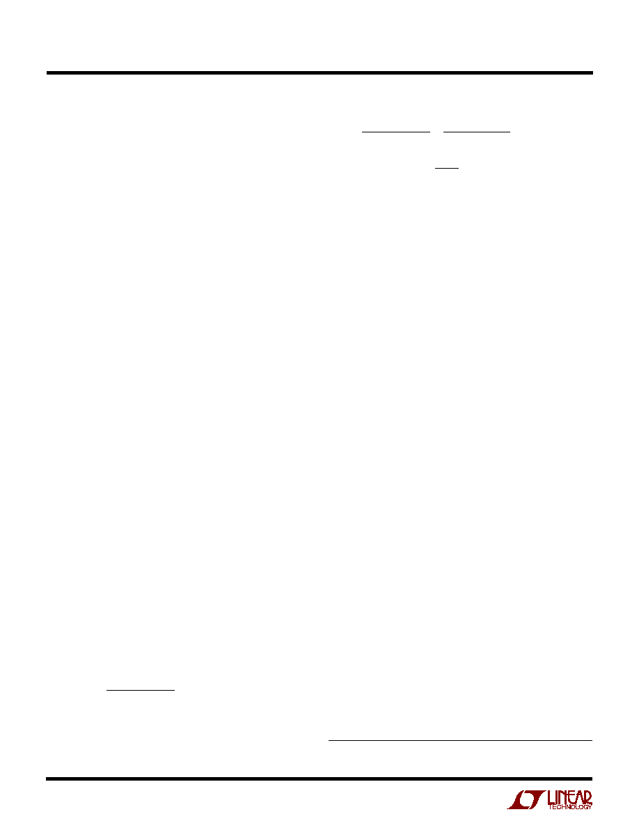
20
LTC1702
tantalum capacitors specifically designed for use with
switching regulators. When choosing a tantalum input
capacitor, make sure that it is rated to carry the RMS
current that the LTC1702 will draw. If the data sheet
doesn't give an RMS current rating, chances are the
capacitor isn't surge tested. Don't use it!
OUTPUT BYPASS CAPACITOR
The output bypass capacitor has quite different require-
ments from the input capacitor. The ripple current at the
output of a buck regulator like the LTC1702 is much lower
than at the input, due to the fact that the inductor current
is constantly flowing at the output whenever the LTC1702
is operating in continuous mode. The primary concern at
the output is capacitor ESR. Fast load current transitions
at the output will appear as voltage across the ESR of the
output bypass capacitor until the feedback loop in the
LTC1702 can change the inductor current to match the
new load current value. This ESR step at the output is often
the single largest budget item in the load regulation
calculation. As an example, our hypothetical 1.6V, 10A
switcher with a 0.01
ESR output capacitor would expe-
rience a 100mV step at the output with a 0 to 10A load
step--a 6.3% output change!
Usually the solution is to parallel several capacitors at the
output. For example, to keep the transient response inside
of 3% with the previous design, we'd need an output ESR
better than 0.0048
. This can be met with three 0.014
,
470
Ķ
F low ESR tantalum capacitors in parallel.
INDUCTOR
The inductor in a typical LTC1702 circuit is chosen prima-
rily for value and saturation current. The inductor value
sets the ripple current, which is commonly chosen at
around 40% of the anticipated full load current. Ripple
current is set by:
I
t
V
L
RIPPLE
ON Q
OUT
=
(
)
(
)
2
In our hypothetical 1.6V, 10A example, we'd set the ripple
current to 40% of 10A or 4A, and the inductor value would
be:
APPLICATIO
N
S I
N
FOR
M
ATIO
N
W
U
U
U
L
t
V
I
s
V
A
H
with t
V
V
kHz
s
ON Q
OUT
RIPPLE
ON Q
=
(
)
=
Ķ
(
)( )
=
Ķ
= -
=
Ķ
(
)
(
)
.
.
.
.
/
.
2
2
1 2
1 6
4
0 5
1
1 6
5
550
1 2
The inductor must not saturate at the expected peak
current. In this case, if the current limit was set to 15A, the
inductor should be rated to withstand 15A + 1/2 I
RIPPLE
,
or 17A without saturating.
FEEDBACK LOOP/COMPENSATION
1
Feedback Loop Types
In a typical LTC1702 circuit, the feedback loop consists of
the modulator, the external inductor and output capacitor,
and the feedback amplifier and its compensation network.
All of these components affect loop behavior and need to
be accounted for in the loop compensation. The modulator
consists of the internal PWM generator, the output MOSFET
drivers and the external MOSFETs themselves. From a
feedback loop point of view, it looks like a linear voltage
transfer function from COMP to SW and has a gain roughly
equal to the input voltage. It has fairly benign AC behavior
at typical loop compensation frequencies with significant
phase shift appearing at half the switching frequency.
The external inductor/output capacitor combination makes
a more significant contribution to loop behavior. These
components cause a second order LC roll-off at the
output, with the attendant 180
į
phase shift. This roll-off is
what filters the PWM waveform, resulting in the desired
DC output voltage, but the phase shift complicates the
loop compensation if the gain is still higher than unity at
the pole frequency. Eventually (usually well above the LC
pole frequency), the reactance of the output capacitor will
approach its ESR, and the roll-off due to the capacitor will
stop, leaving 6dB/octave and 90
į
of phase shift (Figure 8).
So far, the AC response of the loop is pretty well out of the
user's control. The modulator is a fundamental piece of the
LTC1702 design, and the external L and C are usually
chosen based on the regulation and load current require-
ments without considering the AC loop response. The
1
The information in this section is based on the paper "The K Factor: A New Mathematical Tool for
Stability Analysis and Synthesis" by H. Dean Venable, Venable Industries, Inc. For complete paper,
see "Reference Reading #4" at www.linear-tech.com.
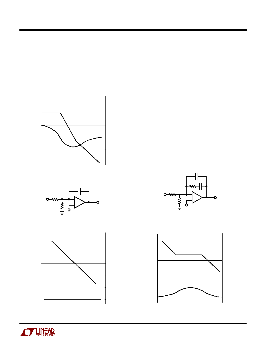
21
LTC1702
APPLICATIO
N
S I
N
FOR
M
ATIO
N
W
U
U
U
feedback amplifier, on the other hand, gives us a handle
with which to adjust the AC response. The goal is to have
180
į
phase shift at DC (so the loop regulates) and some-
thing less than 360
į
phase shift at the point that the loop
gain falls to 0dB. The simplest strategy is to set up the
feedback amplifier as an inverting integrator, with the 0dB
frequency lower than the LC pole (Figure 9). This "type 1"
OUT
IN
R1
C2
C1
R2
R
B
1702 F10a
V
REF
+
≠
GAIN
(dB)
PHASE
(DEG)
1702 F10b
0
0
≠90
≠180
≠270
PHASE
GAIN
≠6dB/OCT
≠6dB/OCT
Figure 10a. Type 2 Amplifier Schematic Diagram
Figure 10b. Type 2 Amplifier Transfer Function
configuration is stable but transient response will be less
than exceptional if the LC pole is at a low frequency.
Figure 10 shows an improved "type 2" circuit that uses an
additional pole-zero pair to temporarily remove 90
į
of
phase shift. This allows the loop to remain stable with 90
į
more phase shift in the LC section, provided the loop
reaches 0dB gain near the center of the phase "bump."
Type 2 loops work well in systems where the ESR zero in
the LC roll-off happens close to the LC pole, limiting the
total phase shift due to the LC. The additional phase
compensation in the feedback amplifier allows the 0dB
point to be at or above the LC pole frequency, improving
loop bandwidth substantially over a simple type 1 loop. It
has limited ability to compensate for LC combinations
where low capacitor ESR keeps the phase shift near 180
į
for an extended frequency range. LTC1702 circuits using
conventional switching grade electrolytic output capaci-
tors can often get acceptable phase margin with type 2
compensation.
GAIN
(dB)
PHASE
(DEG)
1702 F08
A
V
0
0
≠90
≠180
≠6dB/OCT
PHASE
GAIN
≠12dB/OCT
Figure 8. Transfer Function of Buck Modulator
OUT
IN
R1
C1
R
B
1702 F09a
V
REF
+
≠
GAIN
(dB)
PHASE
(DEG)
1702 F09b
0
0
≠90
≠180
≠270
GAIN
PHASE
≠6dB/OCT
Figure 9a. Type 1 Amplifier Schematic Diagram
Figure 9b. Type 1 Amplifier Transfer Function
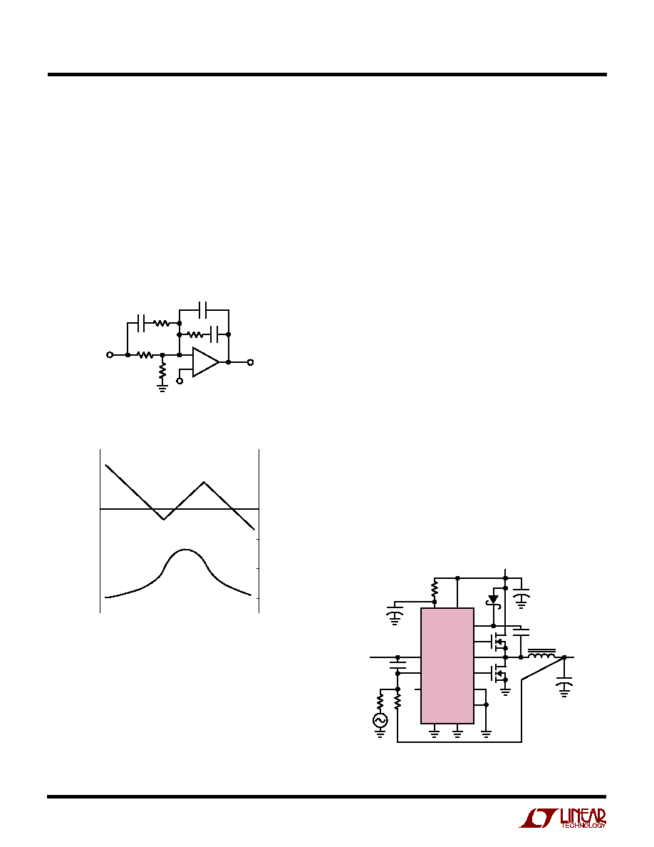
22
LTC1702
Applications that require optimized transient response will
need to recalculate the compensation values specifically
for the circuit in question. The underlying mathematics are
complex, but the component values can be calculated in a
straightforward manner if we know the gain and phase of
the modulator at the crossover frequency.
Modulator gain and phase can be measured directly from
a breadboard, or can be simulated if the appropriate
parasitic values are known. Measurement will give more
accurate results, but simulation can often get close enough
to give a working system. To measure the modulator gain
and phase directly, wire up a breadboard with an LTC1702
and the actual MOSFETs, inductor, and input and output
capacitors that the final design will use. This breadboard
should use appropriate construction techniques for high
speed analog circuitry: bypass capacitors located close to
the LTC1702, no long wires connecting components,
appropriately sized ground returns, etc. Wire the feedback
amplifier as a simple type 1 loop, with a 10k resistor from
V
OUT
to FB and a 0.1
Ķ
F feedback capacitor from COMP to
FB. Choose the bias resistor (R
B
) as required to set the
desired output voltage. Disconnect R
B
from ground and
connect it to a signal generator or to the source output of
a network analyzer (Figure 12) to inject a test signal into
the loop. Measure the gain and phase from the COMP pin
to the output node at the positive terminal of the output
capacitor. Make sure the analyzer's input is AC coupled so
that the DC voltages present at both the COMP and V
OUT
"Type 3" loops (Figure 11) use two poles and two zeros to
obtain a 180
į
phase boost in the middle of the frequency
band. A properly designed type 3 circuit can maintain
acceptable loop stability even when low output capacitor
ESR causes the LC section to approach 180
į
phase shift
well above the initial LC roll-off. As with a type 2 circuit, the
loop should cross through 0dB in the middle of the phase
bump to maximize phase margin. Many LTC1702 circuits
using low ESR tantalum or OS-CON output capacitors
need type 3 compensation to obtain acceptable phase
margin with a high bandwidth feedback loop.
APPLICATIO
N
S I
N
FOR
M
ATIO
N
W
U
U
U
OUT
IN
R1
R3
C2
C1
C3
R2
R
B
1702 F11a
V
REF
+
≠
GAIN
(dB)
PHASE
(DEG)
1702 F11b
0
0
≠90
≠180
≠270
+6dB/OCT
≠6dB/OCT
PHASE
GAIN
≠6dB/OCT
Figure 11a. Type 3 Amplifier Schematic Diagram
Figure 11B. Type 3 Amplifier Transfer Function
BOOST2
TG
SW
BG
FCB
FAULT
COMP
FB
RUN/SS
1/2 LTC1702
V
CC
10
MBR0530T
C
IN
5V
QT
1
Ķ
F
V
OUT
TO
ANALYZER
V
COMP
TO
ANALYZER
AC
SOURCE
FROM
ANALYZER
L
EXT
QB
10
Ķ
F
0.1
Ķ
F
R
B
PV
CC
SGND PGND
+
+
10k
NC
C
OUT
1702 F12
+
Figure 12. Modulator Gain/Phase Measurement Set-Up
Feedback Component Selection
Selecting the R and C values for a typical type 2 or type 3
loop is a nontrivial task. The applications shown in this data
sheet show typical values, optimized for the power com-
ponents shown. They should give acceptable performance
with similar power components, but can be way off if even
one major power component is changed significantly.
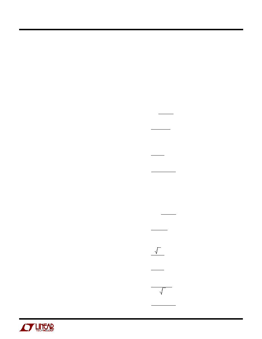
23
LTC1702
Finally, choose a convenient resistor value for R1 (10k is
usually a good value). Now calculate the remaining values:
(K is a constant used in the calculations)
= chosen crossover frequency
G = 10
(GAIN/20)
(this converts GAIN in dB to G in absolute
gain)
Type 2 Loop:
K
Tan
BOOST
C
GKR
C
C K
R
K
C
R
V
R
V
V
B
REF
OUT
REF
=
+ į
=
=
( )
=
=
( )
2
45
2
1
2
1
1
2
1
2
2
1
1
2
≠
≠
Type 3 Loop:
K
Tan
BOOST
C
GR
C
C K
R
K
C
R
R
K
C
K R
R
V
R
V
V
B
REF
OUT
REF
=
+ į
=
=
( )
=
=
( )
=
=
( )
2
4
45
2
1
2
1
1
2
1
2
2
1
3
1
1
3
1
2
3
1
≠
≠
≠
APPLICATIO
N
S I
N
FOR
M
ATIO
N
W
U
U
U
nodes don't corrupt the measurements or damage the
analyzer.
If breadboard measurement is not practical, a SPICE
simulation can be used to generate approximate gain/
phase curves. Plug the expected capacitor, inductor and
MOSFET values into the following SPICE deck and gener-
ate an AC plot of V(V
OUT
)/V(COMP) in dB and phase of
V(OUT) in degrees. Refer to your SPICE manual for details
of how to generate this plot.
*1702 modulator gain/phase
*
©
1999 Linear Technology
*this file written to run with PSpice 8.0
*may require modifications for other SPICE
simulators
*MOSFETs
rfet mod sw 0.02
;MOSFET rdson
*inductor
lext sw out1 1u
;inductor value
rl out1 out 0.005
;inductor series R
*output cap
cout out out2 1000u
;capacitor value
resr out2 0 0.01
;capacitor ESR
*1702 internals
emod mod 0 comp 0 5
;3.3 for 3.3V supply
vstim comp 0 0 ac 1
;ac stimulus
.ac dec 100 1k 1meg
.probe
.end
With the gain/phase plot in hand, a loop crossover fre-
quency can be chosen. Usually the curves look something
like Figure 8. Choose the crossover frequency in the rising
or flat parts of the phase curve, beyond the external LC
poles. Frequencies between 10kHz and 50kHz usually
work well. Note the gain (GAIN, in dB) and phase (PHASE,
in degrees) at this point. The desired feedback amplifier
gain will be ≠ GAIN to make the loop gain 0dB at this
frequency. Now calculate the needed phase boost, assum-
ing 60
į
as a target phase margin:
BOOST = ≠ (PHASE + 30
į
)
If the required BOOST is less than 60
į
, a type 2 loop can
be used successfully, saving two external components.
BOOST values greater than 60
į
usually require type 3
loops for satisfactory performance.

24
LTC1702
Accuracy Trade-Offs
The V
DS
sensing scheme used in the LTC1702 is not
particularly accurate, primarily due to uncertainty in the
R
DS(ON)
from MOSFET to MOSFET. A second error term
arises from the ringing present at the SW pin, which
causes the V
DS
to look larger than (I
LOAD
)(R
DS(ON)
) at the
beginning of QB's on-time. These inaccuracies do not
prevent the LTC1702 current limit circuit from protecting
itself and the load from damaging overcurrent conditions,
but they do prevent the user from setting the current limit
to a tight tolerance if more than one copy of the circuit is
being built. The 50% factor in the current setting equation
above reflects the margin necessary to ensure that the
circuit will stay out of current limit at the maximum normal
load, even with a hot MOSFET that is running quite a bit
higher than its R
DS(ON)
spec.
FCB OPERATION/SECONDARY WINDINGS
The FCB pin can be used in conjunction with a secondary
winding on one side of the LTC1702 to generate a third
regulated voltage output. This output can be directly
regulated at the FCB pin. In theory, a fourth output could
be added, either unregulated or with additional external
circuitry at the FCB pin.
The extra auxiliary output is taken from a second winding
on the core of the inductor on one channel, converting it
into a transformer (Figure 13). The auxiliary output voltage
is set by the main output voltage and the turns ratio of the
extra winding to the primary winding. Load regulation at
the auxiliary output will be relatively good as long as the
main output is running in continuous mode. As the load on
the main channel drops and the LTC1702 switches to
discontinuous or Burst Mode operation, the auxiliary
output will not be able to maintain regulation, especially if
the load at the auxiliary output remains heavy.
To avoid this, the auxiliary output voltage can be divided
down with a conventional feedback resistor string with the
divided auxiliary output voltage fed back to the FCB pin
(Figure 13). The FCB pin threshold is trimmed to 800mV
APPLICATIO
N
S I
N
FOR
M
ATIO
N
W
U
U
U
CURRENT LIMIT PROGRAMMING
Programming the current limit on the LTC1702 is straight-
forward. The I
MAX
pin sets the current limit by setting the
maximum allowable voltage drop across QB (the bottom
MOSFET) before the current limit circuit engages. The
voltage across QB is set by its on-resistance and the
current flowing in the inductor, which is the same as the
output current. The LTC1702 current limit circuit inverts
the voltage at I
MAX
before comparing it with the negative
voltage across QB, allowing the current limit to be set with
a positive voltage.
To set the current limit, calculate the expected voltage drop
across QB at the maximum desired current:
V
I
R
mV
PROG
ILIM
DS ON
=
( )
(
)
+
(
)
100
I
LIM
should be chosen to be quite a bit higher than the
expected operating current, to allow for MOSFET R
DS(ON)
changes with temperature. Setting I
LIM
to 150% of the
maximum normal operating current is usually safe and will
adequately protect the power components if they are
chosen properly. The 100mV term is an approximate
factor that corrects for errors caused by ringing on the
switch node (illustrated in Figure 6). This factor will
change depending on the layout and the components
used, but 100mV is usually a good starting point. V
DROP
is
then programmed at the I
MAX
pin using the internal 10
Ķ
A
pull-up and an external resistor:
R
ILIM
= V
PROG
/10
Ķ
A
The resulting value of R
ILIM
should be checked in an actual
circuit to ensure that the I
LIM
circuit kicks in as expected.
MOSFET R
DS(ON)
specs are like horsepower ratings in
automobiles, and should be taken with a grain of salt.
Circuits that use very low values for R
IMAX
(< 20k) should
be checked carefully, since small changes in R
IMAX
can
cause large I
LIM
changes when the 100mV correction
factor makes up a large percentage of the total V
PROG
value. If V
PROG
is set too low, the LTC1702 may fail to start
up.

25
LTC1702
The FAULT pin is an additional open-drain output that
indicates if one or both of the outputs has exceeded 15%
of its programmed output voltage. FAULT includes an
internal 10
Ķ
A pull-up to V
CC
and does not require an
external pull-up to interface to standard logic. FAULT pulls
low in normal operation, and releases when a overvoltage
fault is detected.
When an overvoltage fault occurs, an internal latch sets
and FAULT goes high, disabling the LTC1702 until the
latch is cleared by recycling the power or pulling both
RUN/SS pins low simultaneously. Alternately, the FAULT
pin can be pulled back low externally with an open-
collector/open-drain device or an NFET or NPN, which will
allow the LTC1702 to resume normal operation, but will
not reset the latch. If the pull-down is later removed, the
LTC1702 will latch off again unless the latch is reset by
cycling the power or RUN/SS pins.
Note that both the PGOOD pins and the FAULT pin monitor
the output voltages by watching the FB pins. During
normal operation, each FB pin is held at a virtual ground by
the feedback amplifier, and changes at the output will not
appear at FB. This is not an issue with a properly designed
circuit, since the virtual ground at FB implies that the
output voltage is under control. If the feedback amplifier
loses control of the output, the virtual ground disappears
and the PGOOD circuit can see any output changes. This
occurs whenever the soft-start or current limit circuits are
active, whenever the MIN or MAX comparators are active,
or any time the feedback amplifier output (the COMP pin)
hits a rail or is in slew limit. Since the MAX comparator will
engage well before the output reaches the +15% fault
level, the FAULT output is largely unaffected by the virtual
ground at FB.
OPTIMIZING PERFORMANCE
2-Step Conversion
The LTC1702 is ideally suited for use in 2-step conversion
systems. 2-step systems use a primary regulator to con-
vert the input power source (batteries or AC line voltage)
APPLICATIO
N
S I
N
FOR
M
ATIO
N
W
U
U
U
with 10mV of hysteresis, allowing fairly precise control of
the auxiliary voltage. If the LTC1702 is in discontinuous or
Burst Mode operation and the auxiliary output voltage
drops, the FCB pin will trip and the LTC1702 will resume
continuous operation regardless of the load on the main
output. The FCB pin removes the requirement that power
must be drawn from the inductor primary in order to
extract power from the auxiliary windings. With the loop in
continuous mode, the auxiliary outputs may be loaded
without regard to the primary load. Note that if the LTC1702
is already running in continuous mode and the auxiliary
output drops due to excessive loading, no additional
action can be taken by the LTC1702 to regulate the
auxiliary output.
POWER GOOD/FAULT FLAGS
The PGOOD pins report the status of the output voltage at
their respective outputs. Each is an open-drain output that
pulls low until the FB pin rises to (V
REF
≠ 5%), indicating
that the output voltage has risen to within 5% of the
programmed output voltage. Each PGOOD pin can inter-
face directly to standard logic inputs if an appropriate pull-
up resistor is added, or the two pins can be tied together
with a single pull-up to give a "both good" signal. Each
PGOOD pin includes an internal 100
Ķ
s delay to prevent
glitches at the output from indicating false PGOOD
signals.
Figure 13. Regulating an Auxiliary Output with the FCB Pin
+
TG
LTC1702
BG
FCB
C
OUT
R
FCB1
+
C
OUT(AUX)
V
OUT(AUX)
1702 F08
+
C
IN
QT
QB
V
OUT
V
IN
R
FCB2
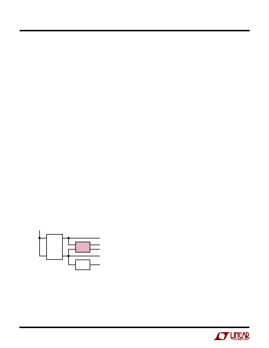
26
LTC1702
to an intermediate supply voltage, often 5V. The LTC1702
then converts the intermediate voltage to the low voltage,
high current supplies required by the system. Compared
to a 1-step converter that converts a high input voltage
directly to a very low output voltage, the 2-step converter
exhibits superior transient response, smaller component
size and equivalent efficiency. Thermal management and
layout complexity are also improved with a 2-step
approach.
A typical notebook computer supply might use a 4-cell
Li-Ion battery pack as an input supply with a 15V nominal
terminal voltage. The logic circuits require 5V/3A and 3.3V/
5A to power system board logic, and 2.5V/0.5A, 1.8V/2A
and 1.5V/10A to power the CPU. A typical 2-step conver-
sion system would use a step-down switcher (perhaps an
LTC1628 or two LTC1625s) to convert 15V to 5V and
another to convert 15V to 3.3V (Figure 14). One channel of
the LTC1702 would generate the 1.5V supply using the
3.3V supply as the input and the other channel would gen-
erate 1.8V using the 5V supply as the input. The corre-
sponding 1-step system would use four similar step-down
switchers, each using 15V as the input supply and gener-
ating one of the four output voltages. Since the 2.5V sup-
ply represents a small fraction of the total output power,
either system can generate it from the 3.3V output using
an LDO linear regulator, without the 75% linear efficiency
making much of an impact on total system efficiency.
APPLICATIO
N
S I
N
FOR
M
ATIO
N
W
U
U
U
Clearly, the 5V and 3.3V sections of the two schemes are
equivalent. The 2-step system draws additional power
from the 5V and 3.3V outputs, but the regulation tech-
niques and trade-offs at these outputs are similar. The
difference lies in the way the 1.8V and 1.5V supplies are
generated. For example, the 2-step system converts 3.3V
to 1.5V with a 45% duty cycle. During the QT on-time, the
voltage across the inductor is 1.8V and during the QB
on-time, the voltage is 1.5V, giving roughly symmetrical
transient response to positive and negative load steps. The
1.8V maximum voltage across the inductor allows the use
of a small 0.47
Ķ
H inductor while keeping ripple current
under 4A (40% of the 10A maximum load). By contrast,
the 1-step converter is converting 15V to 1.5V, requiring
just a 10% duty cycle. Inductor voltages are now 13.5V
when QT is on and 1.5V when QB is on, giving vastly
different di/dt values and correspondingly skewed tran-
sient response with positive and negative current steps.
The narrow 10% duty cycle usually requires a lower
switching frequency, which in turn requires a higher value
inductor and larger output capacitor. Parasitic losses due
to the large voltage swing at the source of QT cost
efficiency, eliminating any advantage the 1-step conver-
sion might have had.
Note that power dissipation in the LTC1702 portion of a
2-step circuit is lower than it would be in a typical 1-step
converter, even in cases where the 1-step converter has
higher total efficiency than the 2-step system. In a typical
microprocessor core supply regulator, for example, the
regulator is usually located right next to the CPU. In a
1-step design, all of the power dissipated by the core
regulator is right there next to the hot CPU, aggravating
thermal management. In a 2-step LTC1702 design, a
significant percentage of the power lost in the core regu-
lation system happens in the 5V or 3.3V supply, which is
usually away from the CPU. The power lost to heat in the
LTC1702 section of the system is relatively low, minimiz-
ing the heat near the CPU.
Figure 14. 2-Step Conversion Block Diagram
V
BAT
15V
LTC1628*
*OR TWO LTC1625s
LTC1702
LDO
5V/3A
1.8V/2A
1.5V/10A
3.3V/5A
2.5V/0.5A
1702 F14
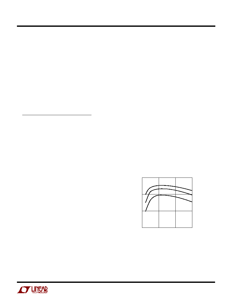
27
LTC1702
2-Step Efficiency Calculation
Calculating the efficiency of a 2-step converter system
involves some subtleties. Simply multiplying the effi-
ciency of the primary 5V or 3.3V supply by the efficiency
of the 1.8V or 1.5V supply underestimates the actual
efficiency, since a significant fraction of the total power is
drawn from the 3.3V and 5V rails in a typical system. The
correct way to calculate system efficiency is to calculate
the power lost in each stage of the converter, and divide the
total output power from all outputs by the sum of the
output power plus the power lost:
Efficiency
TotalOutputPower
TotalOutputPower
TotalPowerLost
=
+
(
)
100%
In our example 2-step system, the total output power is:
Total output power =
15W + 16.5W + 1.25W + 3.6W + 15W = 51.35W
corresponding to 5V, 3.3V, 2.5V, 1.8V and 1.5V output
voltages.
Assuming the LTC1702 provides 90% efficiency at each
output, the additional load on the 5V and 3.3V supplies is:
1.5V: 15W/90% = 16.6W/3.3V = 5A from 3.3V
1.8V: 3.6W/90% = 4W/5V = 0.8A from 5V
2.5V: 1.25W/75% = 1.66W/3.3V = 0.5A from 3.3V
If the 5V and 3.3V supplies are each 94% efficient, the
power lost in each supply is:
1.5V: 16.6W ≠ 15W = 1.6W
1.8V: 4W ≠ 3.6W = 0.4W
2.5V: 1.66W ≠ 1.25W = 0.4W
3.3V: 17.55W ≠ 16.5W = 1W
5V:
16W ≠ 15W = 1W
Total loss = 4.4W
Total system efficiency =
51.35W/(51.35W + 4.4W) = 92.1%
APPLICATIO
N
S I
N
FOR
M
ATIO
N
W
U
U
U
Maximizing High Load Current Efficiency
Efficiency at high load currents (when the LTC1702 is
operating in continuous mode) is primarily controlled by
the resistance of the components in the power path
(QT, QB, L
EXT
) and power lost in the gate drive circuits due
to MOSFET gate charge. Maximizing efficiency in this
region of operation is as simple as minimizing these
terms.
The behavior of the load over time affects the efficiency
strategy. Parasitic resistances in the MOSFETs and the
inductor set the maximum output current the circuit can
supply without burning up. A typical efficiency curve
(Figure 15) shows that peak efficiency occurs near 30% of
this maximum current. If the load current will vary around
the efficiency peak and will spend relatively little time at the
maximum load, choosing components so that the average
load is at the efficiency peak is a good idea. This puts the
maximum load well beyond the efficiency peak, but usually
gives the greatest system efficiency over time, which
translates to the longest run time in a battery-powered
system. If the load is expected to be relatively constant at
the maximum level, the components should be chosen so
that this load lands at the peak efficiency point, well below
the maximum possible output of the converter.
Figure 15. Typical LTC1702 Efficiency Curves
LOAD CURRENT (A)
0
70
EFFICIENCY (%)
80
90
100
5
10
1702 G01
15
V
IN
= 5V
V
OUT
= 3.3V
V
OUT
= 2.5V
V
OUT
= 1.6V

28
LTC1702
Maximizing Low Load Current Efficiency
Low load current efficiency depends strongly on proper
operation in discontinuous and Burst Mode operations. In
an ideally optimized system, discontinuous mode reduces
conduction losses but not switching losses, since each
power MOSFET still switches on and off once per cycle. In
a typical system, there is additional loss in discontinuous
mode due to a small amount of residual current left in the
inductor when QB turns off. This current gets dissipated
across the body diode of either QT or QB. Some LTC1702
systems lose as much to body diode conduction as they
save in MOSFET conduction. The real efficiency benefit of
discontinuous mode happens when Burst Mode operation
is invoked. At typical power levels, when Burst Mode
operation is activated, gate drive is the dominant loss
term. Burst Mode operation turns off all output switching
for several clock cycles in a row, significantly cutting gate
drive losses. As the load current in Burst Mode operation
falls toward zero, the current drawn by the circuit falls to
the LTC1702's background quiescent level--about 3mA
per channel.
To maximize low load efficiency, make sure the LTC1702
is allowed to enter discontinuous and Burst Mode opera-
tion as cleanly as possible. FCB must be above its 0.8V
threshold. Minimize ringing at the SW node so that the
discontinuous comparator leaves as little residual current
in the inductor as possible when QB turns off. It helps to
connect the SW pin of the LTC1702 as close to the drain
of QB as possible. An RC snubber network can also be
added from SW to PGND.
REGULATION OVER COMPONENT TOLERANCE/
TEMPERATURE
DC Regulation Accuracy
The LTC1702 initial DC output accuracy depends mainly
on internal reference accuracy, op amp offset and external
resistor accuracy. Two LTC1702 specs come into play:
feedback voltage and feedback voltage line regulation. The
feedback voltage spec is 800mV
Ī
8mV over the full
temperature range, and is specified at the FB pin, which
encompasses both reference accuracy and any op amp
offset. This accounts for 1% error at the output with a 5V
input supply. The feedback voltage line regulation spec
adds an additional 0.05%/V term that accounts for change
in reference output with change in input supply voltage.
With a 5V supply, the errors contributed by the LTC1702
itself add up to no more than 1% DC error at the output.
The output voltage setting resistors (R1 and R
B
in
Figure 3) are the other major contributor to DC error. At a
typical 1.xV output voltage, the resistors are of roughly the
same value, which tends to halve their error terms, im-
proving accuracy. Still, using 1% resistors for R1 and R
B
will add 1% to the total output error budget, equal to that
of all errors due to the LTC1702 combined. Using 0.1%
resistors in just those two positions can nearly halve the
DC output error for very little additional cost.
Load Regulation
Load regulation is affected by feedback voltage, feedback
amplifier gain and external ground drops in the feedback
path. Feedback voltage is covered above and is within 1%
over temperature. A full-range load step might require a
10% duty cycle change to keep the output constant,
requiring the COMP pin to move about 100mV. With
amplifier gain at 85dB, this adds up to only a 10
Ķ
V shift at
FB, negligible compared to the reference accuracy terms.
External ground drops aren't so negligible. The LTC1702
can sense the positive end of the output voltage by
attaching the feedback resistor directly at the load, but it
cannot do the same with the ground lead. Just 0.001
of
resistance in the ground lead at 10A load will cause a 10mV
error in the output voltage--as much as all the other DC
errors put together. Proper layout becomes essential to
achieving optimum load regulation from the LTC1702.
See the Layout/Troubleshooting section for more infor-
mation. A properly laid out LTC1702 circuit should move
less than a millivolt at the output from zero to full load.
TRANSIENT RESPONSE
Transient response is the other half of the regulation
equation. The LTC1702 can keep the DC output voltage
constant to within 1% when averaged over hundreds of
APPLICATIO
N
S I
N
FOR
M
ATIO
N
W
U
U
U
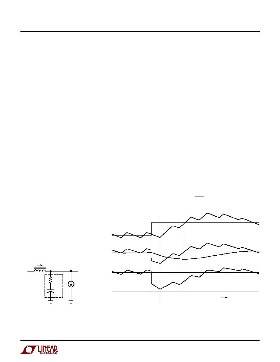
29
LTC1702
cycles. Over just a few cycles, however, the external
components conspire to limit the speed that the output
can move. Consider our typical 5V to 1.6V circuit, sub-
jected to a 1A to 5A load transient. Initially, the loop is in
regulation and the DC current in the output capacitor is
zero. Suddenly, an extra 4A start flowing out of the output
capacitor while the inductor is still supplying only 1A. This
sudden change will generate a (4A)(C
ESR
)voltage step at
the output; with a typical 0.015
output capacitor ESR,
this is a 60mV step at the output, or 3.8% (for a 1.6V output
voltage).
Very quickly, the feedback loop will realize that something
has changed and will move at the bandwidth allowed by
the external compensation network towards a new duty
cycle. If the bandwidth is set to 50kHz, the COMP pin will
get to 60% of the way to 90% duty cycle in 3
Ķ
s. Now the
inductor is seeing 3.5V across itself for a large portion of
the cycle, and its current will increase from 1A at a rate set
by di/dt = V/L. If the inductor value is 0.5
Ķ
H, the di/dt will
be 3.5V/0.5
Ķ
H or 7A/
Ķ
s. Sometime in the next few micro-
seconds after the switch cycle begins, the inductor current
will have risen to the 5A level of the load current and the
output capacitor will stop losing charge.
Note that the output voltage will stop dropping before the
inductor current reaches this new output current level.
Recall that any practical output capacitor looks like a pure
capacitance in series with some amount of ESR. When a
load transient hits, virtually all of the initial voltage drop at
the output is due to IR drop across the ESR. The output
capacitance begins to discharge at the same time and
continues until the inductor current rises to match the new
output current level.
The output voltage, however, will turn around and start
heading the right way before this happens. The next time
the top MOSFET turns on, the inductor current will begin
increasing linearly. This increasing current flows almost
entirely into the capacitor, going through the ESR as it
does so (Figure 16). Positive di/dt in the inductor causes
positive dv/dt in the ESR, regardless of what the "pure"
capacitance is doing. The output voltage will turn around
when the positive dv/dt across the ESR exceeds the
negative dv/dt across the pure capacitance. If the expected
load step (
I) is known, an optimum inductor value can be
chosen:
L
V
V
C
ESR
I
IN
OUT
(
)
≠
∑ ∑
APPLICATIO
N
S I
N
FOR
M
ATIO
N
W
U
U
U
+
≠
≠
I
L
V
OUT
I
OUT
1702 F16a
V
ESR
C
OUT
V
CAP
V
SW
L
+
V
CAP
V
OUT
TRANSIENT
HITS
V
OUT
TURNS
AROUND
I
L
> I
OUT
TIME
V
ESR
I
OUT
I
L
V
OUT
V
ESR
I
OUT
I
L
V
CAP
V
OUT(NOMINAL)
1702 F16b
Figure 16b. Transient Recovery Curves
Figure 16a. Capacitor Parasitics
Affecting Transient Recovery

30
LTC1702
APPLICATIO
N
S I
N
FOR
M
ATIO
N
W
U
U
U
Making L smaller than this optimum value yields little or no
improvement in transient response. As the output voltage
recovers, the inductor current will briefly rise above the
level of the output current to replenish the charge lost from
the output capacitor. With a properly compensated loop,
the entire recovery time will be inside of 10
Ķ
s.
Most loads care only about the maximum deviation from
ideal, which occurs somewhere in the first two cycles after
the load step hits. During this time, the output capacitor
does all the work until the inductor and control loop regain
control. The initial drop (or rise if the load steps down) is
entirely controlled by the ESR of the capacitor and amounts
to most of the total voltage drop. To minimize this drop,
reduce the ESR as much as possible by choosing low ESR
capacitors and/or paralleling multiple capacitors at the
output. The capacitance value accounts for the rest of the
voltage drop until the inductor current rises. With most
output capacitors, several devices paralleled to get the
ESR down will have so much capacitance that this drop
term is negligible. Ceramic capacitors are an exception; a
small ceramic capacitor can have suitably low ESR with
relatively small values of capacitance, making this second
drop term significant.
Optimizing Loop Compensation
Loop compensation has a fundamental impact on tran-
sient recovery time, the time it takes the LTC1702 to
recover after the output voltage has dropped due to output
capacitor ESR. Optimizing loop compensation entails
maintaining the highest possible loop bandwidth while
ensuring loop stability. The Feedback Component Selec-
tion section describes in detail how to design an optimized
feedback loop, appropriate for most LTC1702 systems.
Voltage Positioning
If the load transients consist primarily of load steps from
near zero load to full load and back, the transient response
can be traded off against DC regulation performance by
using a technique known as "voltage positioning." The
goal is to intentionally compromise the DC regulation loop
such that the output rides near the maximum allowable
value (often +5%) with no load and near the minimum
allowable value at maximum load. With the load at zero,
any transient that comes along will be a current increase
which will cause the output voltage to fall. Since the output
voltage is initially at a high value, it can fall further before
LTC1702
FB
1702 F17a
1702 F17b
V
OUT
V
IN
+5%
≠5%
NOM
MAX
0
V
OUT
LOAD
CURRENT
MAXIMUM
ALLOWABLE
TRANSIENT
Figure 17a. Standard Regulator
Figure 17b. Standard Regulator--Transient Response
LTC1702
FB
1702 F17c
1702 F17d
V
OUT
V
IN
+5%
≠5%
NOM
MAX
0
V
OUT
LOAD
CURRENT
Figure 17c. Voltage Positioning Regulator
Figure 17d. Positioning Regulator--Transient Response
MAXIMUM
ALLOWABLE
TRANSIENT
2
◊
FIGURE 17b
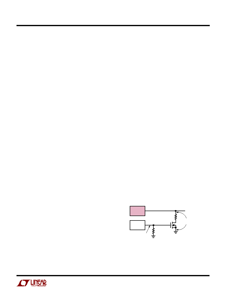
31
LTC1702
it goes out of spec. Similarly, at full load, the output current
can only decrease, causing a positive shift in the output
voltage; the initial low value allows it to rise further before
the spec is exceeded. The primary benefit of voltage
positioning is it increases the allowable ESR of the output
capacitors, saving cost. An additional bonus is that at
maximum load, the output voltage is near the minimum
allowable, decreasing the power dissipated in the load.
Implementing voltage positioning is as simple as creating
an intentional resistance in the output path to generate the
required voltage drop. This resistance can be a low value
resistor, a length of PCB trace, or even the parasitic
resistance of the inductor if an appropriate filter is used. If
the LTC1702 senses the output voltage upstream from the
resistance (Figure 17), the output voltage will move with
load as I ∑ R, where I is the load current and R is the value
of the resistance. If the feedback network is then reset to
regulate near the upper edge of the specified tolerance, the
output voltage will ride high when I
LOAD
is low and will ride
low when I
LOAD
is high. Compared to a traditional regula-
tor, a voltage positioning regulator can theoretically stand
as much as twice the ESR drop across the output capacitor
while maintaining output voltage regulation. This means
smaller, cheaper output capacitors can be used while
keeping the output voltage within acceptable limits.
Measurement Techniques
Measuring transient response presents a challenge in
two respects: obtaining an accurate measurement and
generating a suitable transient to use to test the circuit.
Output measurements should be taken with a scope
probedirectly across the output capacitor. Proper high
frequency probing techniques should be used. In particu-
lar, don't use the 6" ground lead that comes with the
probe! Use an adapter that fits on the tip of the probe and
has a short ground clip to ensure that inductance in the
ground path doesn't cause a bigger spike than the tran-
sient signal being measured. Conveniently, the typical
probe tip ground clip is spaced just right to span the leads
of a typical output capacitor. In general, it is best to take
this measurement with the 20MHz bandwidth limit on the
oscilloscope turned on to limit high frequency noise. Note
that microprocessor manufacturers typically specify ripple
20MHz, as energy above 20MHz is generally radiated
and not conducted and will not affect the load even if it
appears at the output capacitor.
Now that we know how to measure the signal, we need to
have something to measure. The ideal situation is to use
the actual load for the test, and switch it on and off while
watching the output. If this isn't convenient, a current step
generator is needed. This generator needs to be able to
turn on and off in nanoseconds to simulate a typical
switching logic load, so stray inductance and long clip
leads between the LTC1702 and the transient generator
must be minimized.
Figure 18 shows an example of a simple transient genera-
tor. Be sure to use a noninductive resistor as the load
element--many power resistors use an inductive spiral
pattern and are not suitable for use here. A simple solution
is to take ten 1/4W film resistors and wire them in parallel
to get the desired value. This gives a noninductive resistive
load which can dissipate 2.5W continuously or 50W if
pulsed with a 5% duty cycle, enough for most LTC1702
circuits. Solder the MOSFET and the resistor(s) as close to
the output of the LTC1702 circuit as possible and set up
the signal generator to pulse at a 100Hz rate with a 5% duty
cycle. This pulses the LTC1702 with 500
Ķ
s transients
10ms apart, adequate for viewing the entire transient
recovery time for both positive and negative transitions
while keeping the load resistor cool.
APPLICATIO
N
S I
N
FOR
M
ATIO
N
W
U
U
U
Figure 18. Transient Load Generator
LTC1702
PULSE
GENERATOR
1702 F18
IRFZ44 OR
EQUIVALENT
50
0V TO 10V
100Hz, 5%
DUTY CYCLE
V
OUT
R
LOAD
LOCATE CLOSE
TO THE OUTPUT
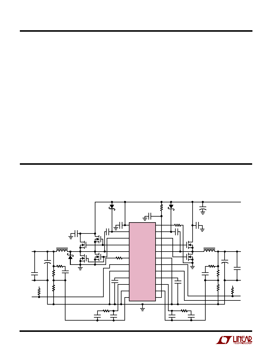
32
LTC1702
APPLICATIO
N
S I
N
FOR
M
ATIO
N
W
U
U
U
FAULT BEHAVIOR
Changing the Output Voltage on the Fly
Some applications use a switching scheme attached to the
feedback resistors to allow the system to adjust the
LTC1702 output voltage. The voltage can be changed on
the fly if desired, but care must be taken to avoid tripping
the overvoltage fault circuit. Stepping the voltage upwards
abruptly is safe, but stepping down quickly by more than
15% can leave the system in a state where the output
voltage is still at the old higher level, but the feedback node
is set to expect a new, substantially lower voltage. If this
condition persists for more than 10
Ķ
s, the overvoltage
fault circuitry will fire and latch off the LTC1702.
The simplest solution is to disable the fault circuit by
grounding the FAULT pin. Systems that must keep the
fault circuit active should ensure that the output voltage is
never programmed to step down by more than 15% in any
single step. The safest strategy is to step the output down
by 10% or less at a time and wait for the output to settle
to the new value before taking subsequent steps.
VID Applications
Certain microprocessors specify a set of codes that corre-
spond to power supply voltages required from the regula-
tor system. If these codes are changed on the fly, the same
caveats as above apply. In addition, the switching matrix
that programs the output voltage may vary its resistance
significantly over the entire span of output voltages,
potentially changing the loop compensation if the circuit is
not designed properly. With a typical type 3 feedback loop
(Figure 8), make sure that the R
BIAS
resistor is modified to
set the output voltage. The R1 resistor must stay constant
to ensure that the loop compensation is not affected.
TYPICAL APPLICATIO
N
S
U
3.3V
IN
, 2.5V/1.8V Output Power Supply
LTC1702
PV
CC
BOOST1
BG1
TG1
SW1
I
MAX1
PGOOD1
FCB
RUN/SS
COMP1
SGND
FB1
I
MAX2
BOOST2
BG2
TG2
SW2
PGND
PGOOD2
FAULT
RUN/SS2
COMP2
FB2
V
CC
C5
1
Ķ
F
R1
10
C6
1
Ķ
F
C8
1
Ķ
F
R2 39k
R8
36k
R10
2.4k
R9 27k
1702 TA02
R3
4.3k
R4
10k
1%
C11
820pF
C9
20pF
C10
100pF
R7 68k
C15
1
Ķ
F
V
OUT2
1.8V
12A
C7 1
Ķ
F
R5
8.06k
1%
10k
Q2A
Q2B
Q1B
Q1A
D3
D2
D1, D2: MOTOROLA MBR0520LT1
D3: MOTOROLA MBRS320T3
C1: KEMET T510X477M006AS
C12, C20: PANASONIC EEFUE0G181R
L1: SUMIDA CEP1254712-T007
L2: SUMIDA CDRH744734-JPS023
Q1A, Q1B, Q2A, Q2B: SILICONIX Si9804
Q3, Q4: 1/2 SILICONIX Si4966
D1
GND
L1
0.68
Ķ
H
C12
180
Ķ
F
◊
3
C4
10
Ķ
F
C3
1
Ķ
F
C2
1
Ķ
F
C16 1
Ķ
F
C1
470
Ķ
F
◊
2
+
Q3
Q4
C19
1000pF
C17
100pF
C18
1000pF
R12
10.7k
1%
R13
4.99k
1%
L2
1
Ķ
H
C20
180
Ķ
F
C21
1
Ķ
F
V
OUT1
2.5V
5A
GND
V
IN
V
IN
FAULT
PGOOD2
V
IN
3.3V
Ī
5%
+
+
PGOOD1
10k
33
LTC1702
TYPICAL APPLICATIO
N
S
U
BOOST1
TG1
SW1
BG1
I
MAX1
COMP1
FB1
RUN/SS1
BOOST2
TG2
SW2
BG2
I
MAX2
COMP2
FB2
RUN/SS2
LTC1702
V
CC
PV
CC
GND
PGND
+
+
+
V
OUT1
1.8V
10A
C
OUT1
470
Ķ
F
◊
2
R11
10k
0.1%
C11
330pF
R
B1
7.96k
0.1%
C21
680pF
C31
560pF
L
EXT1
1
Ķ
H
12A
L
EXT2
2.2
Ķ
H 6A
R31, 4.7k
R21, 13k
Q11
Q21
D
CP2
MBR0530T
D
CP1
MBR0530T
C
CP1
1
Ķ
F
C
CP2
1
Ķ
F
D2 MBR330T
1
Ķ
F
R
IMAX1
, 22k
C
SS1
0.1
Ķ
F
C
SS2
0.1
Ķ
F
10
C
IN
470
Ķ
F
◊
2
Q12
Q22
V
OUT2
3.3V
3A
C
OUT2
470
Ķ
F
C12
120pF
C22
270pF
R22, 20k
1702 TA05
R
B2
1.62k
0.1%
R12
4.99k
0.1%
C32
820pF
R32, 2.2k
Q11, Q21: FAIRCHILD FDS6670A
Q12, Q22: 1/2 SILICONIX Si9402
C
IN
, C
OUT1
, C
OUT2
: KEMET T510X477M006AS
R
IMAX2
, 47k
V
IN
= 5V
Ī
10%
L
EXT1
: MURATA LQT12535C1ROM12
L
EXT2
: COILTRONICS UP2B-2R2
28W Dual Output Power Supply

34
LTC1702
TYPICAL APPLICATIO
N
S
U
Single Output, 2-Phase, Minimum Capacitors 5V to 2.5V/40A Converter
QT1A
C
IN1
10
Ķ
F
◊
2
D1
D2
1
Ķ
F
QT1B
QT2A
QT2B
0.004
0.5W
0.004
0.5W
V
IN
5V
Ī
10%
0.004
0.5W
0.004
0.5W
C
IN1
, C
OUT
, C
VCC
: MURATA GRM235Y5V106Z
C
IN2
: AVX TPSD107M010R0080
D1, D2, D3: MOTOROLA MBR0530T1
ALL MOSFETS: FAIRCHILD FDS6670A
L1, L2: SUMIDA CEP125-0R47
C
IN2
100
Ķ
F
+
V
CC
PV
CC
L
TC1702
10
10k
10k
10
D3
SGND
PGND
FB1
COMP1
FB2
COMP2
PGOOD1
PGOOD2
RUN/SS1
RUN/SS2
FCB
F
AUL
T
TG1
TG2
BOOST1
SW1
BOOST2
SW2
I
MAX1
I
MAX2
BG1
BG2
C
VCC
10
Ķ
F
0.01
Ķ
F
0.01
Ķ
F
4.7k
10k
10k
10k
1%
100k
4.75k
0.1%
0.1
Ķ
F
0.1
Ķ
F
0.1
Ķ
F
1
Ķ
F
0.1
Ķ
F
V
IN
QB1A
QB1B
QB2A
QB2B
L2 0.47
Ķ
H
L1 0.47
Ķ
H
≠
+
L
T1006
33k
33k
PGOOD
C
OUT
10
Ķ
F
CER
◊
4
V
OUT
2.5V
40A
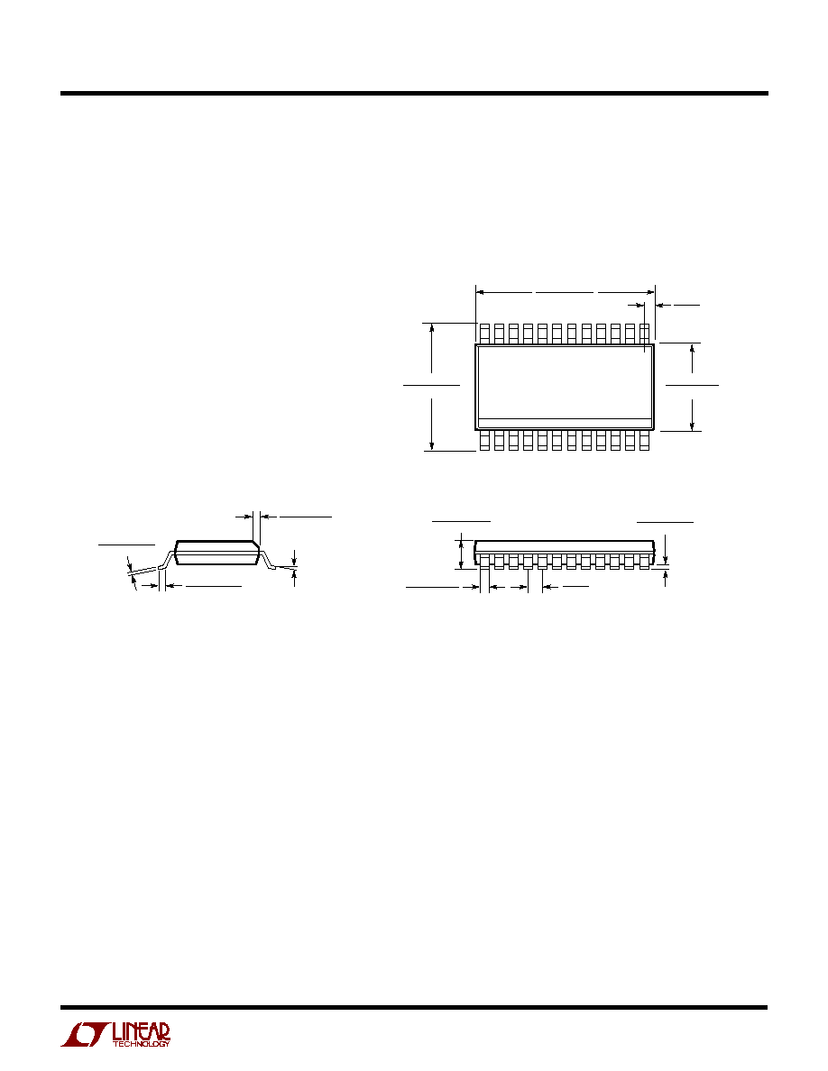
35
LTC1702
PACKAGE DESCRIPTIO
N
U
Dimensions in inches (millimeters) unless otherwise noted.
GN Package
24-Lead Plastic SSOP (Narrow 0.150)
(LTC DWG # 05-08-1641)
0.337 ≠ 0.344*
(8.560 ≠ 8.738)
GN24 (SSOP) 1098
* DIMENSION DOES NOT INCLUDE MOLD FLASH. MOLD FLASH
SHALL NOT EXCEED 0.006" (0.152mm) PER SIDE
** DIMENSION DOES NOT INCLUDE INTERLEAD FLASH. INTERLEAD
FLASH SHALL NOT EXCEED 0.010" (0.254mm) PER SIDE
1
2
3
4
5
6
7
8
9 10 11 12
0.229 ≠ 0.244
(5.817 ≠ 6.198)
0.150 ≠ 0.157**
(3.810 ≠ 3.988)
16
17
18
19
20
21
22
23
24
15 1413
0.016 ≠ 0.050
(0.406 ≠ 1.270)
0.015
Ī
0.004
(0.38
Ī
0.10)
◊
45
į
0
į
≠ 8
į
TYP
0.007 ≠ 0.0098
(0.178 ≠ 0.249)
0.053 ≠ 0.068
(1.351 ≠ 1.727)
0.008 ≠ 0.012
(0.203 ≠ 0.305)
0.004 ≠ 0.0098
(0.102 ≠ 0.249)
0.0250
(0.635)
BSC
0.033
(0.838)
REF
Information furnished by Linear Technology Corporation is believed to be accurate and reliable.
However, no responsibility is assumed for its use. Linear Technology Corporation makes no represen-
tation that the interconnection of its circuits as described herein will not infringe on existing patent rights.
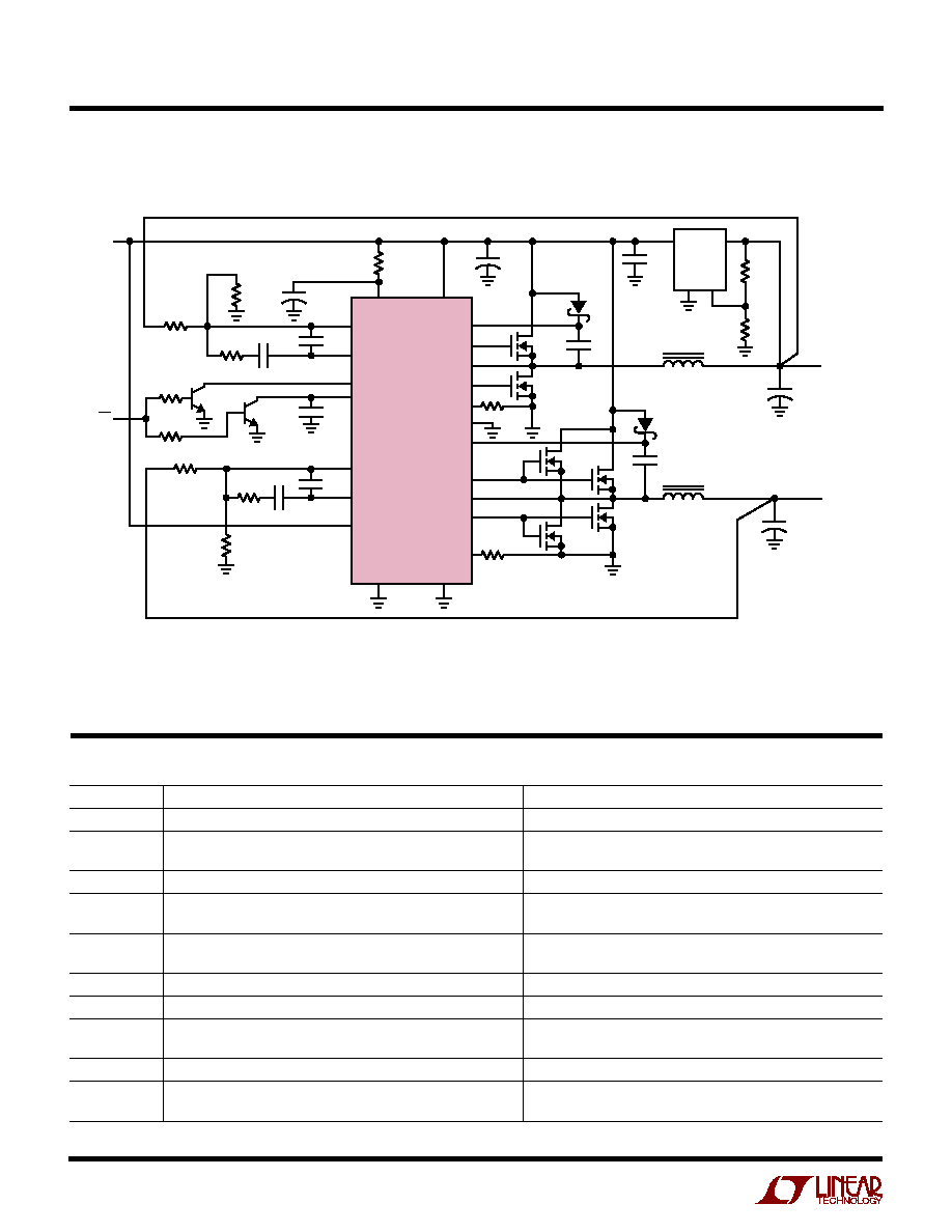
36
LTC1702
1702f LT/TP 0100 4K ∑ PRINTED IN USA
©
LINEAR TECHNOLOGY CORPORATION 1999
Linear Technology Corporation
1630 McCarthy Blvd., Milpitas, CA 95035-7417
(408) 432-1900
q
FAX: (408) 434-0507
q
www.linear-tech.com
TYPICAL APPLICATIO
N
U
RELATED PARTS
PART NUMBER
DESCRIPTION
COMMENTS
LTC1530
High Power Synchronous Step-Down Controller
SO-8 with Current Limit. No R
SENSE
Required
LTC1625
No R
SENSE
TM
Current Mode Synchronous Step-Down Controller
Above 95% Efficiency, Needs No R
SENSE
, 16-Lead SSOP Package
Fits SO-8 Footprint
LTC1628
Dual High Efficiency 2-Phase Synchronous Step-Down Controller
Constant Frequency, Standby 5V and 3.3V LDOs, 3.5V
V
IN
36V
LTC1703
Dual 550kHz Synchronous 2-Phase Switching Regulator Controller LTC1702 with 5-Bit Mobile VID for Mobile Pentium
ģ
Processor
with Mobile VID
Systems
LTC1706-81
VID Voltage Programmer
Adds 5-Bit Mobile VID to 0.8V Referenced Switching
Regulators
LTC1709
2-Phase, 5-Bit Desktop VID Synchronous Step-Down Controller
Current Mode, V
IN
to 36V, I
OUT
Up to 42A
LTC1736
Synchronous Step-Down Controller with 5-Bit Mobile VID Control
Fault Protection, PowerGood, 3.5V to 36V Input, Current Mode
LTC1753
5-Bit Desktop VID Programmable Synchronous
1.3V to 3.5V Programmable Output Using Internal 5-Bit DAC
Switching Regulator
LTC1873
Dual Synchronous Switching Regulator with 5-Bit Desktop VID
1.3V to 3.5V Programmable Core Output Plus I/O Output
LTC1929
2-Phase, Synchronous High Efficiency Converter
Current Mode Ensures Accurate Current Sensing,
V
IN
Up to 36V, I
OUT
Up to 40A
No R
SENSE
is a trademark of Linear Technology Corporation. Pentium is a registered trademark of Intel Corporation.
Low Cost Dual Supply with 2.5V Keepalive
+
FB2
COMP2
RUN/SS2
FB1
COMP1
FCB
BOOST2
TG2
SW2
BG2
I
MAX2
V
CC
PV
CC
SGND
PGND
LTC1702
4.75k
0.1%
0.1
Ķ
F
39pF
56pF
220pF
330pF
56k
20k
1%
16k
1%
QSS2
QSS1
C
IN
= SANYO 10MV1200GX (6 IN PARALLEL)
C
OUT1
= SANYO 6MV1500GX (8 IN PARALLEL)
C
OUT2
= SANYO 6MV1500GX (3 IN PARALLEL)
L1: 1
Ķ
H SUMIDA CEP125-1R0MC-H
L2: 2.2
Ķ
H COILTRONICS UP2B-2R2
V
IN
5V
Ī
10%
STBY/ON
1k
68k
1k
10k
0.1%
47k
QT2
MBR0530T
1
Ķ
F
QB2
QT1A
QT1B
MBR0530T
1
Ķ
F
C
OUT1
1702 TA04
+
C
OUT2
+
10
Ķ
F
+
C
IN
1
Ķ
F
16.9k
0.1%
16.2k
0.1%
V
OUT2
2.5V/7A
2.45V/100mA
STANDBY
V
OUT1
1.8V
20A
10
L1
QB1A
QB1B
33k
FAULT
BOOST1
TG1
SW1
BG1
I
MAX1
L2
IN
OUT
GND
LT1761
ADJ
RUN/SS1
QSS1, QSS2: MOTOROLA MMBT3904LT1
QT1A, QT1B, QB1A, QB1B: FAIRCHILD FDS6670A
QT2, QB2: 1/2 SILICONIX Si4966