Äîêóìåíòàöèÿ è îïèñàíèÿ www.docs.chipfind.ru
LTC1706-82
1
Information furnished by Linear Technology Corporation is believed to be accurate and reliable.
However, no responsibility is assumed for its use. Linear Technology Corporation makes no represen-
tation that the interconnection of its circuits as described herein will not infringe on existing patent rights.
Final Electrical Specifications
The LTC
®
1706-82 is a precision, digitally programmed,
resistive ladder which adjusts the output of any 0.8V
referenced regulator. Depending on the state of the five
VID inputs, an output voltage between 1.10V and 1.85V is
programmed in 25mV increments.
The LTC1706-82 is designed specifically to program an
entire family of Linear Technology DC/DC converters in full
compliance with the Intel Desktop VID specification.
The LTC1706-82 programs the following Linear Technol-
ogy DC/DC converter products: LTC1622, LTC1628,
LTC1629, LTC1702, LTC1735, LTC1735-1, LTC1772 and
LTC1929.
Consult factory for future compatible DC/DC converter
products.
s
Intel Pentium
®
III Processor Power Supply
s
Multiprocessor Workstations and Servers
s
Multiphase Processor Power Supply
s
AMD Athlon
TM
Processor Power Supply
s
Fully Compliant with the Intel VRM 9.0 VID
Specification
s
Programs Regulator Output Voltage from 1.10V to
1.85V in 25mV Steps
s
Programs an Entire Family of Linear Technology
DC/DC Converters
s
±
0.25% Accurate Voltage Divider
s
Built-In 40k Pull-Up Resistors on Program Inputs
s
Available in MSOP-10 Packaging
APPLICATIO S
U
FEATURES
DESCRIPTIO
U
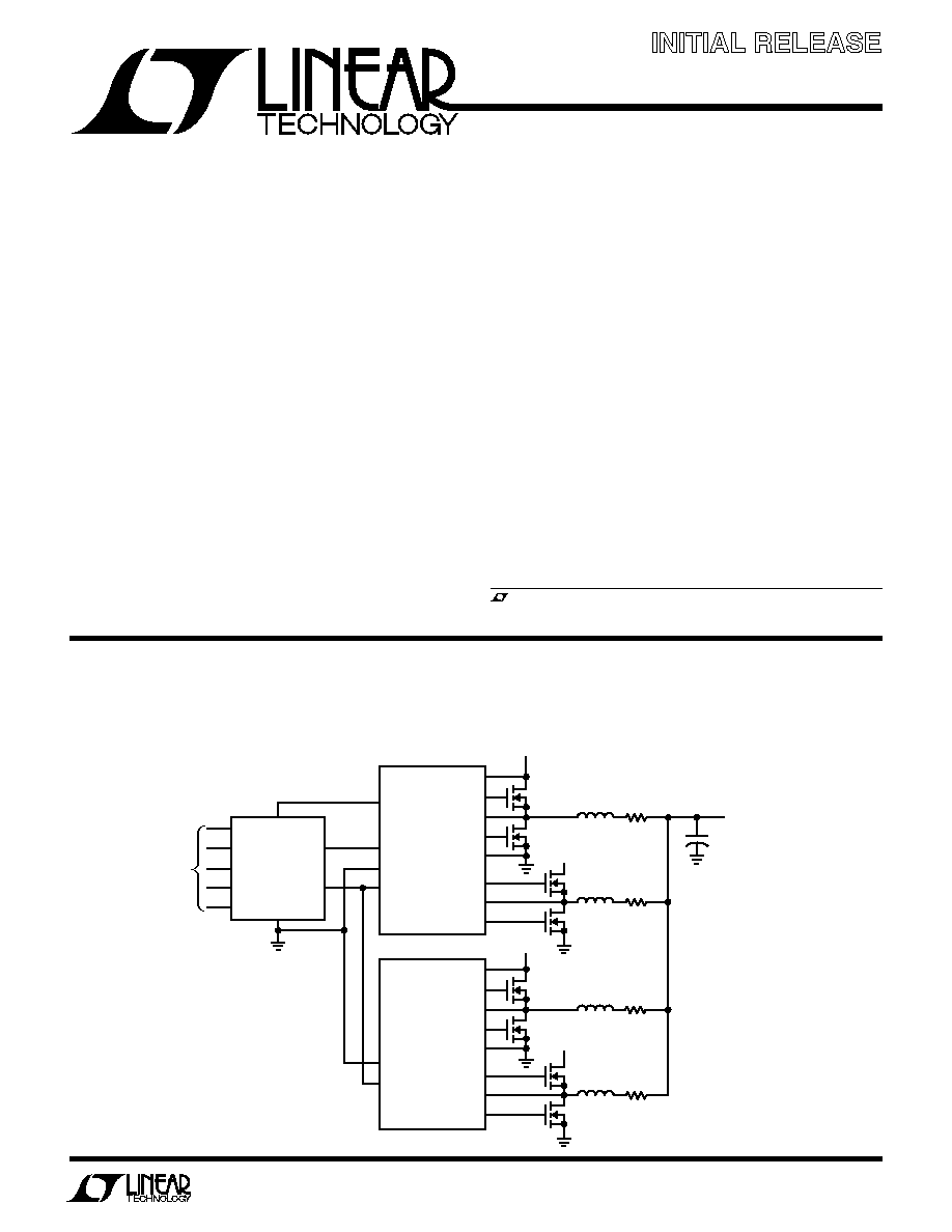
TYPICAL APPLICATIO
U
VID Voltage Programmer
for Intel VRM 9.0
January 2000
1706-82 TA01
L1
R
SENSE1
V
IN
V
IN
4.5V TO 22V
V
IN
4.5V TO 22V
LTC1629
V
DIFFOUT
SGND
EAIN
INTV
CC
C
OUT
V
IN
TG1
SW1
BG1
PGND
+
V
OUT
1.10V TO 1.85V
UP TO 70A
VID0
VID1
VID2
VID3
VID4
V
CC
LTC1706-82
GND
SENSE
FB
FROM
µ
P
L2
R
SENSE2
UP TO SIX LTC1629s CAN BE PARALLELED
TO DELIVER AS MUCH AS 200A
L3
R
SENSE3
V
IN
LTC1629
SGND
EAIN
V
IN
TG1
SW1
BG1
PGND
L4
R
SENSE4
TG2
SW2
BG2
TG2
SW2
BG2
VID Controlled High Current 4-Phase DC/DC Converter (Simplified Block Diagram)
, LTC and LT are registered trademarks of Linear Technology Corporation.
Pentium is a registered trademark of Intel Corporation.
AMD Athlon is a trademark of Advanced Micro Devices, Inc.
LTC1706-82
2
(Voltages Referred to GND Pin)
Input Supply Voltage (V
CC
) .......................... 0.3V to 7V
VID Input Pins ............................................. 0.3V to 7V
SENSE Pin ................................................... 0.3V to 7V
FB Pin .......................................................... 0.3V to 7V
Operating Temperature Range (Note 2) .. 40
°
C to 85
°
C
Junction Temperature ........................................... 110
°
C
Storage Temperature Range ................. 65
°
C to 150
°
C
Lead Temperature (Soldering, 10 sec).................. 300
°
C
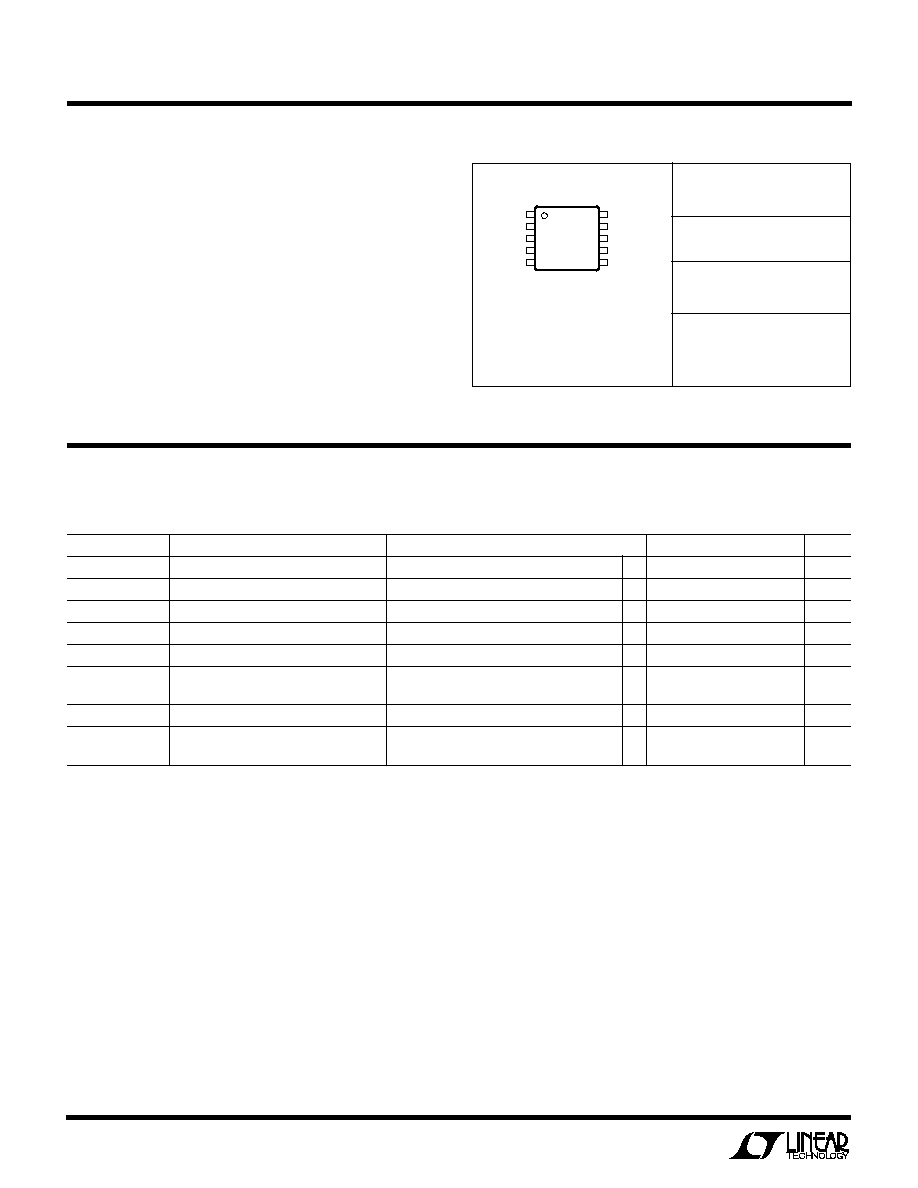
ORDER PART
NUMBER
MS10
PART MARKING
T
JMAX
= 110
°
C,
JA
= 120
°
C/W
Consult factory for Industrial and Military grade parts.
LTMJ
LTC1706EMS-82
ABSOLUTE AXI U
RATI GS
W
W
W
U
PACKAGE/ORDER I FOR ATIO
U
U
W
(Note 1)
ELECTRICAL CHARACTERISTICS
The
q
denotes the specifications which apply over the full operating temperature range, otherwise specifications are at T
A
= 25
°
C.
2.7V
V
CC
5.5V, VIDO = VID1 = VID2 = VID3 = VID4 = NC unless otherwise specified.
SYMBOL
PARAMETER
CONDITIONS
MIN
TYP
MAX
UNITS
V
CC
Operating Supply Voltage Range
2.7
5.5
V
I
VCC
Supply Current
(Note 3)
0.1
5.0
µ
A
R
FB-SENSE
Resistance Between SENSE and FB
q
6
10
14
k
V
OUT
Error %
Output Voltage Accuracy
Programmed From 1.10V to 1.85V
q
0.25
0.25
%
R
PULLUP
VID Input Pull-Up Resistance
V
DIODE
= 0.6V, (Note 4)
40
k
VID
T
VID Input Voltage Threshold
V
IL
(2.7V < V
CC
< 5.5V)
0.4
V
V
IH
(2.7V < V
CC
< 5.5V)
1.6
V
I
VID-LEAK
VID Input Leakage Current
V
CC
< VID < 7V, (Note 4)
0.01
±
1.00
µ
A
V
PULLUP
VID Pull-Up Voltage
V
CC
= 3.3V
2.8
V
V
CC
= 5V
4.5
V
Note 3: With all five VID inputs floating, the V
CC
supply current is simply
the device leakage current. However, the V
CC
supply current will rise and
be approximately equal to the number of grounded VID input pins times
(V
CC
0.6V)/40k. (See the Applications Information section for more
detail.)
Note 4: Each built-in pull-up resistor attached to the VID inputs also has a
series diode connected to V
CC
to allow input voltages higher than the V
CC
supply without damage or clamping. (See Operation section for further
details.)
Note 1: Absolute Maximum Ratings are those values beyond which the life
of a device may be impaired.
Note 2: The LTC1706-82 is guaranteed to meet performance specifications
from 0
°
C to 70
°
C. Specifications over the 40
°
C to 85
°
C operating
temperature range are assured by design, characterization and correlation
with statistical process controls.
1
2
3
4
5
VID0
VID1
VID2
VID3
V
CC
10
9
8
7
6
FB
GND
NC
VID4
SENSE
TOP VIEW
MS10 PACKAGE
10-LEAD PLASTIC MSOP
LTC1706-82
3
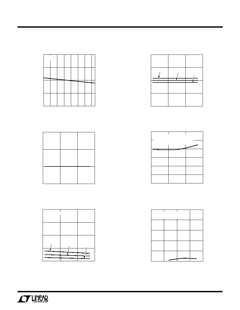
TYPICAL PERFOR A CE CHARACTERISTICS
U
W
Typical Error % vs Output Voltage
Typical Error % vs Temperature
R
FB1
vs Temperature
I
VID-PULLUP
vs Temperature
Supply Current vs Temperature
Supply Current vs Supply Voltage
OUTPUT VOLTAGE (V)
1.1
ERROR (%)
1706-82 G01
0.25
0
0.25
1.2
1.3
1.4
1.5
1.6
1.7
1.8
T
A
= 25
°
C
TEMPERATURE (
°
C)
50
0
50
100
ERROR (%)
1706-82 G02
0.25
0
0.25
V
OUT
= 1.85V
V
OUT
= 1.5V
V
OUT
= 1.1V
TEMPERATURE (
°
C)
50
0
50
100
R
FB1
(k
)
1706-82 G03
30
20
10
0
TEMPERATURE (
°
C)
50
0
50
100
VID PULL-UP CURRENT (
µ
A)
1706-82 G04
120
100
80
60
40
20
0
V
CC
= 5V
VID4 = 0V
VID0 = VID1 = VID2 = VID3 = OPEN
TEMPERATURE (
°
C)
50
0
50
100
SUPPLY CURRENT (
µ
A)
1706-82 G05
2.0
1.5
1.0
0.5
0
V
CC
= 2.7V
V
CC
= 5V
ALL VID INPUTS OPEN
V
CC
= 3.3V
SUPPLY VOLTAGE (V)
0
2
4
6
8
SUPPLY CURRENT (
µ
A)
1706-82 G06
5
4
3
2
1
0
ALL VID INPUTS OPEN
T
A
= 25
°
C
LTC1706-82
4
VID0 (Pin 1): LSB Programming Input. Low = GND,
High = V
CC
or Float. Grounding VID0 adds 25mV to the
output sense voltage.
VID1 (Pin 2): 4th MSB Programming Input. Low = GND,
High = V
CC
or Float. Grounding VID1 adds 50mV to the
output sense voltage.
VID2 (Pin 3): 3rd
MSB Programming Input. Low = GND,
High = V
CC
or Float. Grounding VID2 adds 100mV to the
output sense voltage.
VID3 (Pin 4): 2nd
MSB Programming Input. Low = GND,
High = V
CC
or Float. Grounding VID3 adds 200mV to the
output sense voltage.
V
CC
(Pin 5): Power Supply Voltage. Range from 2.7V to
5.5V.
PI FU CTIO S
U
U
U
SENSE (Pin 6): Regulator Output Voltage. Connect di-
rectly to regulator output sense node or V
DIFFOUT
when
used with the LTC1629 and LTC1929.
VID4 (Pin 7): MSB Programming Input. Low = GND,
High = V
CC
or Float. Grounding VID4 adds 400mV to the
output sense voltage.
NC (PIN 8): No Connect.
GND (Pin 9): Ground. Connect to regulator signal ground.
FB (Pin 10): Feedback Input. Connect to the 0.8V feedback
pin of a compatible regulator or the EAIN pin of the
LTC1629 and LTC1929.
PI
U
TABLE
NOMINAL (V)
ABSOLUTE MAX (V)
PIN
NAME
DESCRIPTION
MIN
TYP
MAX
MIN
MAX
1
VID0
LSB Programmable Input
0
V
CC
0.3
7
2
VID1
3rd MSB Programmable Input
0
V
CC
0.3
7
3
VID2
2nd MSB Programmable Input
0
V
CC
0.3
7
4
VID3
1st MSB Programmable Input
0
V
CC
0.3
7
5
V
CC
Power Supply
2.7
5.5
0.3
7
6
SENSE
Regulator Output Voltage
1.075
1.85
0.3
7
7
VID4
MSB Programmable Input
0
V
CC
0.3
7
8
NC
9
GND
Ground
0
0.3
7
10
FB
0.8V Feedback Input
0
0.8
1.5
0.3
7
LTC1706-82
5
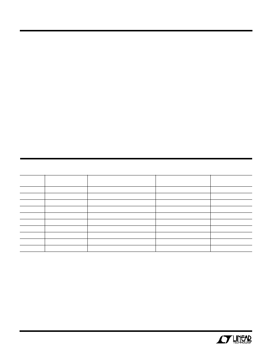
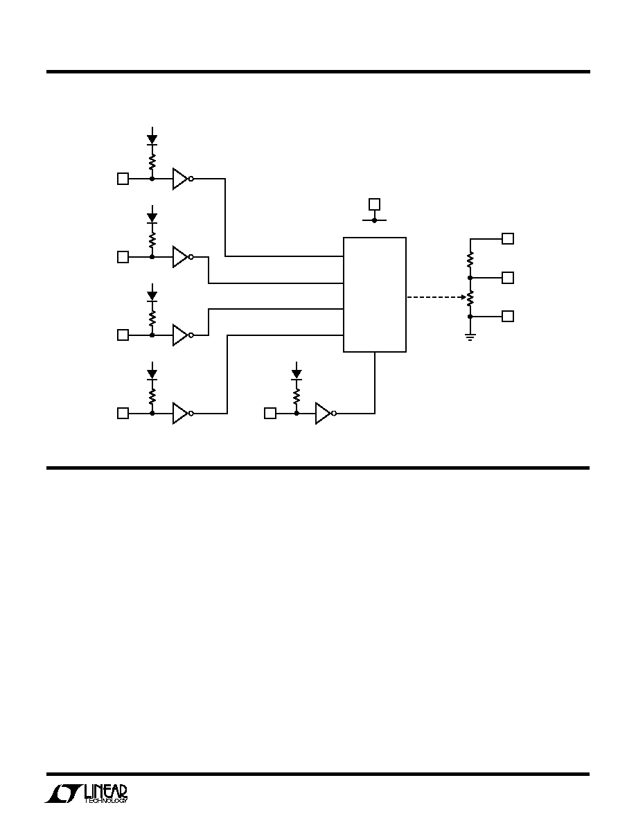
BLOCK DIAGRA
W
OPERATIO
U
The LTC1706-82 is a precision resistive divider designed
specifically for use with an entire family of Linear Technol-
ogy Corporation DC/DC switching regulators with 0.8V
internal reference and feedback voltages. The LTC1706-82
produces an output voltage ranging from 1.10V to 1.85V
in 25mV steps by closing the loop between the output
voltage sense and the feedback input of the regulator with
the appropriate resistive divider network.
The "top" feedback resistor, R
FB1
, connected between
SENSE and FB, is typically 10k and is not modified by the
state of the VID program inputs.
The "bottom" feedback resistor, R
FB2
, however is modi-
fied by the five VID inputs and is precisely ratioed to R
FB1
.
VID Programming
A list of programmed inputs and their corresponding
output voltages is shown in Table 1. Programming is
accomplished by applying the proper voltage (or float
condition) on the five digital VID inputs. VID4 is the most
significant bit (MSB) and VID0 is the least significant bit
(LSB).
When the five VID inputs are low, or grounded, the
regulator output voltage is set to 1.85V. Each increasing
binary count is equivalent to a decrease of 25mV in the
output voltage. Therefore, to obtain a 1.10V output, only
VID0 is grounded while the other four VID inputs are tied
high or floating.
When all five VID inputs are high or floating, such as when
no CPU is present in a system, a regulated 1.075V output
is generated at V
SENSE
.
1706-82 BD
40k
VID3
V
CC
40k
VID4
V
CC
40k
VID2
V
CC
40k
VID1
V
CC
40k
VID0
V
CC
R
FB2
R
FB1
10k
SENSE
FB
GND
V
CC
1
2
3
4
6
5
10
9
7
SWITCH
CONTROL
LOGIC