 | –≠–ª–µ–∫—Ç—Ä–æ–Ω–Ω—ã–π –∫–æ–º–ø–æ–Ω–µ–Ω—Ç: LTC1730 | –°–∫–∞—á–∞—Ç—å:  PDF PDF  ZIP ZIP |
LTC1730-4/LTC1730-4.2
1
sn1730 1730fs
FEATURES
DESCRIPTIO
U
APPLICATIO S
U
TYPICAL APPLICATIO
U
The LTC
Æ
1730 is a complete pulse charger for 1-cell
lithium-ion batteries. When charging a depleted cell, the
internal MOSFET is fully on allowing the current limited
input power source to provide charge current to the
battery, virtually eliminating heat generation in the charger.
As the battery accepts charge and approaches the pro-
grammed voltage, the internal MOSFET begins switching
off and on with the duty cycle gradually decreasing as the
battery approaches a fully charged condition. A program-
mable timer ends the charge cycle. The end-of-charge
condition is indicated at the CHRG pin when the average
charge current falls to C/10. Removing the input voltage
puts the LTC1730 into a sleep mode, dropping the battery
current drain to less than 1
µ
A (maximum).
An external sense resistor limits the maximum charge
current as a safety precaution against a user connecting a
wall adapter with the incorrect or no current limit. The
internal MOSFET prevents reverse battery current from
flowing if the input voltage is shorted to ground, eliminat-
ing the need for a blocking diode.
The LTC1730-4 is available in the 16-pin SSOP package
and the LTC1730-4.2 is available in the 8-pin SO package.
s
Standalone Lithium-Ion Battery Charger
s
Handheld Computers
s
Cellular Telephones
, LTC and LT are registered trademarks of Linear Technology Corporation.
s
Complete Pulse Charger for 1-Cell Lithium-Ion
Batteries
s
Sense Resistor Limits Maximum Current for Safety
s
1% Float Voltage Accuracy
s
End-of-Charge (C/10) Detection Output
s
Programmable Charge Termination Timer
s
Internal 0.35
NMOS Switch
s
No Blocking Diode Required
s
SEL Pin to Set Either 4.1V or 4.2V/Cell (LTC1730-4)
s
Low-Battery Drain (1
µ
A Max) when Input Supply Is
Removed
s
Battery Temperature Sensing and Charge
Qualification
s
Automatic Trickle Charge for Low-Battery
s
Automatic Battery Refresh
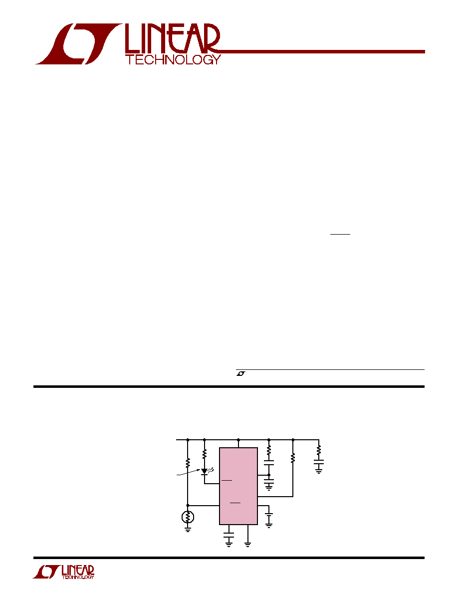
Lithium-Ion Battery
Pulse Charger with
Overcurrent Protection
R1
1k
R2
10k
4.7
R
SENSE
0.05
1-CELL
Li-Ion
BATTERY
D3
R3
4.1k
CHRG
NTC/SHDN
GATE
BAT
TIMER
C
TIMER
0.1
µ
F
GND
5
4
V
CC
2
LTC1730ES8-4.2
SENSE
C1
1
µ
F
C3
0.047
µ
F
0.022
µ
F
3
6
1
7
8
V
IN
= 4.5V TO 12V
WITH 1A CURRENT LIMIT
CHARGE STATUS
1730 TA01
R4
10k
NTC*
T
*NTC: DALE NTHS-1206N02
1A, Single Cell 4.2V Li-Ion Battery Charger (8-Pin Package)

LTC1730-4/LTC1730-4.2
2
sn1730 1730fs
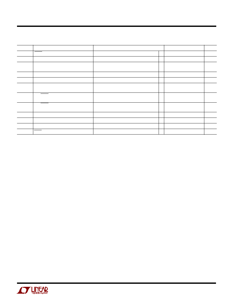
Supply Voltage (V
CC
) ............................................ 13.2V
SENSE, GATE, BAT,
TIMER, NTC/SHDN, SEL ............................ ≠ 0.3V to V
CC
CHRG, ACPR, FAULT ..............................≠ 0.3V to 13.2V
ORDER PART
NUMBER
S8 PART MARKING
T
JMAX
= 125
∞
C,
JA
= 110
∞
C/W
Consult LTC Marketing for parts specified with wider operating temperature ranges.
173042
LTC1730ES8-4.2
ABSOLUTE AXI U
RATI GS
W
W
W
U
(Note 1)
The
q
denotes the specifications which apply over the full operating
temperature range, otherwise specifications are at T
A
= 25
∞
C. V
CC
= 6V unless otherwise noted.
1
2
3
4
8
7
6
5
TOP VIEW
BAT
GATE
NTC/SHDN
TIMER
SENSE
V
CC
CHRG
GND
S8 PACKAGE
8-LEAD PLASTIC SO
SYMBOL
PARAMETER
CONDITIONS
MIN
TYP
MAX
UNITS
V
CC
Supply Voltage
q
4.5
12
V
I
CC
Supply Current
Charger On; Fast Charge Mode
q
2
5
mA
Shutdown: V
NTC/SHDN
= 0V
q
2
5
mA
Sleep Mode; V
BAT
= 4V
q
1
µ
A
V
BAT
Regulated Output Voltage
LTC1730ES8-4.2 (5V
V
CC
12V)
q
4.158
4.2
4.242
V
LTC1730EGN-4 (5V
V
CC
12V), SEL = GND
q
4.059
4.1
4.141
V
LTC1730EGN-4 (5V
V
CC
12V), SEL = V
CC
q
4.158
4.2
4.242
V
I
MAX
Maximum Charge Overcurrent
R
SENSE
= 0.1
q
0.7
1
1.3
A
I
TRICKL
Trickle Charge Current
V
BAT
= 2V
15
35
60
mA
V
TRICKL
Trickle Charge Trip Threshold
2.45
2.55
V
V
ASD
Automatic Shutdown Threshold Voltage
(V
CC
≠ V
BAT
) Low to High
150
mV
(Sleep Mode)
(V
CC
≠ V
BAT
) High to Low
0
mV
R
DS(ON)
Internal Switch On-Resistance
V
BAT
= 4V
0.35
V
SHDN
Shutdown Threshold Voltage
NTC/SHDN Pin High to Low
50
mV
DC ELECTRICAL CHARACTERISTICS
ORDER PART
NUMBER
LTC1730EGN-4
1
2
3
4
5
6
7
8
TOP VIEW
GN PACKAGE
16-LEAD PLASTIC SSOP
16
15
14
13
12
11
10
9
GND*
SENSE
V
CC
ACPR
FAULT
CHRG
NC**
GND*
GND*
BAT
NC**
GATE
SEL
NTC/SHDN
TIMER
GND*
* FOUR CORNER PINS ARE FUSED TO
INTERNAL DIE ATTACH PADDLE FOR
HEAT SINKING. CONNECT THESE FOUR
PINS TO EXPANDED PC LANDS FOR
PROPER HEAT SINKING.
** NO INTERNAL CONNECTION
T
JMAX
= 125
∞
C,
JA
= 90
∞
C/W
Operating Junction
Temperature Range (Note 2) .................. ≠ 40
∞
C to 85
∞
C
Storage Temperature Range ................. ≠ 65
∞
C to 150
∞
C
Lead Temperature (Soldering, 10 sec).................. 300
∞
C
GN PART MARKING
17304
LTC1730-4/LTC1730-4.2
3
sn1730 1730fs
Note 1: Absolute Maximum Ratings are those values beyond which the life
of a device may be impaired.
Note 2: The LTC1730-4/LTC1730-4.2 are guaranteed to meet performance
specifications from 0
∞
C to 70
∞
C. Specifications over the ≠ 40
∞
C to 85
∞
C
SYMBOL
PARAMETER
CONDITIONS
MIN
TYP
MAX
UNITS
I
CHRG
CHRG Pin Pull-Down Current
V
CHRG
= 1V, C/10 Mode
10
40
70
µ
A
T
TIMER
TIMER Accuracy
C
TIMER
= 0.1
µ
F
10
%
V
GATE
GATE Pin Voltage
V
BAT
= 3V
7.5
V
V
BAT
= 4V
10
V
T
SHDN
Thermal Shutdown Temperature
140
∞
C
T
SHDN
Thermal Shutdown Hysteresis
5
∞
C
V
RECHRG
Recharge Battery Voltage Offset from
V
BAT(Full Charged)
≠ V
RECHRG
(Note 3)
150
mV
Full Charged Battery Voltage
V
NTC_HOT
NTC/SHDN Pin Threshold Voltage (Hot)
High to Low; V
CC
= 4V
q
1.95
2
2.05
V
Hysteresis
50
mV
V
NTC_COLD
NTC/SHDN Pin Threshold Voltage (Cold)
Low to High; V
CC
= 4V
q
3.4
3.5
3.6
V
Hysteresis
45
mV
V
SEL
SEL Pin Threshold
LTC173ECGN-4
0.7
V
V
ACPR
ACPR Pin Output Low Voltage
LTC1730EGN-4, I
ACPR
= 5mA
0.6
V
V
FAULT
FAULT Pin Output Low Voltage
LTC1730EGN-4, I
FAULT
= 3mA
1.2
V
V
CHRG
CHRG Pin Output Low Voltage
I
CHRG
= 5mA, Charging Mode
0.9
V
The
q
denotes the specifications which apply over the full operating
temperature range, otherwise specifications are at T
A
= 25
∞
C. V
CC
= 6V unless otherwise noted.
DC ELECTRICAL CHARACTERISTICS
operating temperature range are assured by design, characterization and
correlation with statistical process controls.
Note 3: For the LTC1730-4 version, the full charged V
BAT
value is
typically 4.1V.
LTC1730-4/LTC1730-4.2
4
sn1730 1730fs
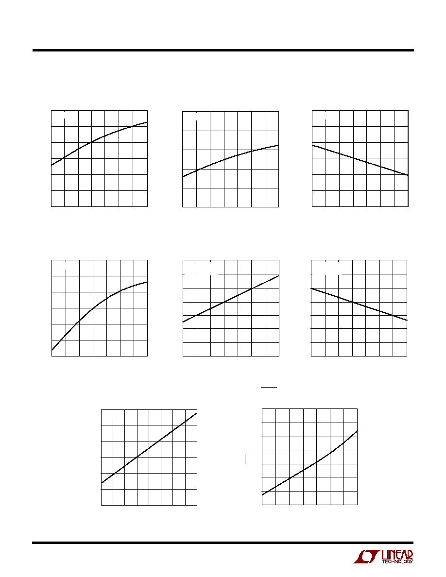
TYPICAL PERFOR A CE CHARACTERISTICS
U
W
V
CC
(V)
5
I (mA)
50
45
40
35
30
25
20
8
10
1730 G01
6
7
9
11
12
TA = 25
∞
C
TEMPERATURE (
∞
C)
≠50
V
TRIKL
(V)
2.50
2.48
2.46
2.44
2.42
2.40
25
75
1730 G02
≠25
0
50
100
125
V
CC
= 6V
TEMPERATURE (
∞
C)
≠50
25
75
1730 G03
≠25
0
50
100
125
I (mA)
50
45
40
35
30
25
20
V
CC
= 6V
Trickle Charge Current vs Input
Supply Voltage
Trickle Charge Current vs
Temperature
Trickle Charge Threshold Voltage
vs Temperature
TEMPERATURE (
∞
C)
≠50
25
75
1730 G05
≠25
0
50
100
125
R
DS(ON)
(
)
0.50
0.45
0.40
0.35
0.30
0.25
0.20
V
BAT
= 4V
TEMPERATURE (
∞
C)
≠50
25
75
1730 G06
≠25
0
50
100
125
t
TIMER
(%)
115
110
105
100
95
90
85
80
V
CC
= 6V
C
TIMER
= 0.1
µ
F
TEMPERATURE (
∞
C)
≠50
25
75
1730 G07
≠25
0
50
100
125
I
MAX
(A)
1.3
1.2
1.1
1.0
0.9
0.8
0.7
0.6
V
CC
= 6V
R
SEN
= 0.1
TEMPERATURE (
∞
C)
≠50
25
75
1730 G08
≠25
0
50
100
125
V
CHRG
(V)
1.0
0.9
0.8
0.7
0.6
0.5
0.4
0.3
Timer Accuracy vs Temperature
Internal Switch On-Resistance vs
Temperature
Overcurrent vs Temperature
CHRG Pin Output Low Voltage vs
Temperature
Battery Recharge Threshold Offset
from V
BAT
vs Temperature
TEMPERATURE (
∞
C)
≠50
25
75
1730 G09
≠25
0
50
100 125 150
V
RECHRG
(mV)
300
250
200
150
100
50
0
V
CC
= 6V

LTC1730-4/LTC1730-4.2
5
sn1730 1730fs
PI FU CTIO S
U
U
U
LTC1730ES8-4.2
SENSE (Pin 1): Maximum Overcurrent Sense Input. A
sense resistor (R
SENSE
) should be connected from V
CC
to
the SENSE pin. When the voltage drop across R
SENSE
exceeds 100mV, the pass transistor immediately turns off
and turns back on after a 400ms time-out period (C
TIMER
= 0.1
µ
F). The on-off cycle will continue, as long as the
overcurrent condition persists or until the timer runs out.
If overcurrent protection is not needed, short SENSE to
V
CC
.
V
CC
(Pin 2): Positive Input Supply Voltage (4.5V
V
CC
13.2V). Bypass this pin with a 1
µ
F capacitor in series with
a 4.7
resistor. An RC network from the V
CC
pin to the
GATE pin is also required. The capacitor controls the slew
rate at the V
CC
pin, while the resistor limits the inrush
current when the input voltage is first applied. When the
pass transistor turns on, V
CC
ramps down in a controlled
manner, with a slope equal to 10
µ
A/C. When the pass
transistor turns off, V
CC
ramps up with a slope of 40
µ
A/C.
CHRG (Pin 3): Open-Drain Charge Status Output. When a
depleted battery is being charged, the CHRG pin is pulled
to ground by an N-MOSFET capable of driving an LED.
Once the duty cycle at the GATE pin drops below 10%, the
N-MOSFET turns off and a weak 40
µ
A current source to
ground turns on to indicate a near end-of-charge (C/10)
condition. When a time-out occurs or the input supply is
removed, the CHRG pin goes high impedance.
GND (Pin 4): Electrical Ground Connection and provides
a thermal path from the IC to the PC board copper. Use
large copper pads and traces for maximum heat transfer.
TIMER (Pin 5): Timer Set Pin. The timer period is set by a
capacitor (C
TIMER
) to ground. The timer period is:
t
TIMER
= (C
TIMER
∑ 3Hr)/(0.1
µ
F). The minimum ON time,
OFF time and the overcurrent time-out period are all set by
the same timer period.
NTC/SHDN (Pin 6): Input to the NTC (Negative Tempera-
ture Coefficient) Thermistor Monitoring and Shutdown
Circuitry. With an external 10k
NTC thermistor to ground
and a 1% resistor to V
CC
, this pin can sense the tempera-
ture of the battery pack and stop charging when the
temperature is out of range. When the voltage at this pin
drops below 0.5 ∑ V
CC
, or 2V at hot temperature or rises
above 0.875 ∑ V
CC
, or 3.5V at cold (with V
CC
= 4V), the
charge cycle is suspended and the internal timer is frozen.
The CHRG pin output status is not affected in this hold
state.
When this pin is pulled below 50mV, the IC goes into the
shutdown mode. The charging stops (the GATE pin is
pulled to ground) the timer is reset and the CHRG pin goes
into a high impedance state.
GATE (Pin 7): Gate Drive Output Pin for Internal and
External Pass Transistors. An external N-MOSFET transis-
tor can be connected in parallel with the internal transistor
to reduce the on-resistance for higher charge current. In
this case, an external blocking diode is required to prevent
damage to the battery if V
CC
is shorted to ground. A 10
µ
A
current source pulls this pin up to the charge pump
potential when turned on and a 40
µ
A current source pulls
it down to ground to turn it off. If an overcurrent condition
is detected, the GATE pin is immediately pulled to ground.
A series RC network from the GATE to the V
CC
pin is
required to control the slew rate at the V
CC
pin when the
switch is turned on or off. The slew rate control prevents
excessive current from the capacitor located in the wall
adapter from flowing into the battery when the pass
transistor is turned on. The voltage at this pin is internally
clamped to 12V above the BAT pin.
BAT (Pin 8): Battery Sense Input Pin. This pin is clamped
to 4.7V if the battery is disconnected while charging. An
internal resistor divider presets the final float voltage to
4.2V.
If the voltage at the BAT pin drops 150mV below final float
voltage after the charge cycle has ended, the timer resets
and a new charge cycle begins.
LTC1730EGN-4
GND (Pins 1, 8, 9, 16): Refer to LTC1730ES8-4.2
SENSE (Pin 2): Refer to LTC1730ES8-4.2
V
CC
(Pin 3): Refer to LTC1730ES8-4.2
ACPR (Pin 4): Wall Adapter Present Open-Drain Output.
When the input voltage (wall adapter) is applied to the
LTC1730, this pin is pulled to ground by an internal

LTC1730-4/LTC1730-4.2
6
sn1730 1730fs
BLOCK DIAGRA
W
PI FU CTIO S
U
U
U
N-channel MOSFET. This output can sink up to 5mA
suitable for driving an LED.
FAULT (Pin 5): Fault Condition Detection Open-Drain
Output. This output can sink up to 3mA suitable for driving
an external LED. The internal N-channel MOSFET pulls this
pin to ground when either one of the following conditions
is detected:
1. The voltage at the NTC pin is out of the normal operation
range. This usually means the battery pack temperature
is too high or too low. Once the temperature is back to
normal, the FAULT pin becomes high impedance.
2. The BAT pin potential stays below 2.45V for more
than 1/4 of the programmed charge time. When this
condition is detected, the FAULT pin is pulled low and
latched.
CHRG (Pin 6): Refer to LTC1730ES8-4.2
NC (Pins 7, 14): No Internal Connection. Connecting these
pins to ground will help transfer heat from the package.
TIMER (Pin 10): Refer to LTC1730ES8-4.2
NTC/SHDN (Pin 11): Refer to LTC1730ES8-4.2
SEL (Pin 12): 4.1V/4.2V Battery Selection Input. Ground-
ing this pin will set the output float voltage to 4.1V, while
connecting to V
CC
will set the voltage to 4.2V.
GATE (Pin 13): Refer to LTC1730ES8-4.2
BAT (Pin 15): Refer to LTC1730ES8-4.2
+
≠
≠
+
LOGIC
RECHRG
ON
C6
C4
40mV
+
≠
+
≠
C7
C3
≠
+
+
≠
C8
121mV
C2
+
≠
C1
OSCILLATOR
CLK
FAULT
V
MIN
I
MAX
STOP
C/10
SHDN
V
BAT
HOT
V
MAX
COLD
ACPR
+
≠
C9
1.21V
R4
R5
+
≠
≠
+
C5
100mV
+
≠
150mV
+
≠
R3
R2
R1
35mA
GATE
BAT
N
SW
NTC/SHDN
TIMER
40
µ
A
N1
Q-PUMP
(3X)
SENSE
0.375R
0.5R
GND
1703 BD
CHRG
V
CC
FAULT
0.125R
ACPR
SEL
4.1V/4.2V

LTC1730-4/LTC1730-4.2
7
sn1730 1730fs
When the battery voltage reaches the final float voltage,
the pass transistor turns off for 100ms (minimum off-
time). It remains off as long as the battery voltage stays
above the float voltage after the 100ms off-time. After the
minimum off-time, if the battery voltage drops below the
float voltage, the pass transistor turns back on for at least
380ms (minimum on-time). As the battery approaches full
charge, the off-time will get longer and the on-time will
stay at 380ms. The voltage at the BAT pin will be slightly
higher than the final float voltage due to the ESR associ-
ated with the battery pack. This voltage level should not
turn on the overvoltage protection circuitry often located
in the battery pack. When the duty cycle at the GATE pin
drops below 10%, a comparator turns off the N-FET at the
CHRG pin and connects a weak current source (40
µ
A) to
ground to indicate a near end-of-charge (C/10) condition.
The pulse charging will continue until the timer stops.
An external capacitor at the TIMER pin sets the total charge
time, the minimum on- and off-time and the overcurrent
retry period. After a time-out has occurred, the charge
cycle is terminated and the CHRG pin is forced high
impedance. To restart the charge cycle, momentarily pull
the NTC/SHDN pin below 50mV or remove and reapply the
input voltage. After the charging stops, if the battery
voltage drops 150mV below the final float voltage, due to
external loading or internal leakage, a new charge cycle
will automatically begins.
The charger can be shut down by pulling the NTC/SHDN
pin to ground. When the input voltage is not present, the
charger goes into a sleep mode, dropping battery drain
current to less than 1
µ
A.
The LTC1730 is a complete lithium-ion battery pulse
charger with an internal 0.35
N-MOSFET switch driven
by an internal charge pump. The charge current is set by
the current limit of the input supply (wall adapter). An
external R
SENSE
sets the maximum allowable charge over
current (I
MAX
= 0.1V/R
SENSE
) and prevents a wall adapter
with the wrong current limit from damaging the battery. If
the current limit of the input supply is above I
MAX
, the
charging will be immediately terminated and will retry after
400ms (C
TIMER
= 0.1
µ
F). If the battery is disconnected
while in fast charge mode, the N-channel MOSFET turns
off when the voltage at the BAT pin rises above 4.7V, and
turns back on when the voltage drops below the float
voltage.
A charge cycle begins when the voltage at the V
CC
pin rises
above the BAT pin by 40mV and the voltage at the NTC/
SHDN pin is in between 0.5 ∑ V
CC
and 0.875 ∑ V
CC
. The
charger will go into trickle charge mode if the battery
voltage is below 2.45V. The trickle charge current is preset
to 35mA and is provided by an internal current source. In
trickle mode, the charge pump and pass transistor are off.
When the battery voltage exceeds 2.45V, the charger goes
into the fast charge mode. In this mode, the charge pump
turns on and ramps up the gate voltage of the pass
transistor turning it on. The voltage at the V
CC
pin then
ramps down to V
BAT
plus the voltage drop across the pass
transistor and R
SENSE
, thus reducing the power dissipa-
tion in the pass transistor. The charge current is deter-
mined by the current limit of the input supply.
OPERATIO
U

LTC1730-4/LTC1730-4.2
8
sn1730 1730fs
Stop Charging
The charger is off when any of the following conditions
exist. The voltage at the V
CC
pin is less than 40mV above
V
BAT
(sleep mode), or the potential at the NTC/SHDN pin
is less than 50mV (shutdown mode). The trickle charge
current source and the internal pass transistor are turned
off. The internal resistor divider is disconnected to reduce
the current drain on the battery when in sleep mode.
Input Voltage (Wall Adapter)
The input voltage to the LTC1730 must have some
method of current limit capability. The current limit level
of the input power source must be lower than the
overcurrent limit (I
MAX
) set by the sense resistor (I
MAX
=
100mV/R
SENSE
). If a wall adapter without current limit is
used, or the current limit level is above I
MAX
, the charger
will turn on briefly and then immediately turn off after the
overcurrent condition is detected. This cycle will be re-
sumed every 400ms (C
TIMER
= 0.1
µ
F) until the total charge
time has run out. If overcurrent protection is not needed,
short the SENSE pin to V
CC
.
Trickle Charge and Defective Battery Detection
At the begining of the charge cycle, if the cell voltage is low
(less than 2.45V) the charger goes into a 35mA trickle
charge mode. If the low cell voltage persists for one
quarter of the total charge time, the battery is considered
defective and the charge cycle is terminated. The CHRG
pin output is then forced to a high impedance state.
Battery Charge Current
The battery charge current is determined by the current
limit of the input supply (wall adapter). However, this
current must not exceed the maximum charge overcurrent,
I
MAX
. If an overcurrent condition is detected, the charging
is immediately terminated, the GATE pin is pulled to
ground and the charge pump turns off. The charging will
resume after a 400ms time off (C
TIMER
= 0.1
µ
F).
Programming the Timer
The programmable timer is used to terminate the charge
and sets the minimum ON/OFF time and the overcurrent
time-off period. The length of the timer is programmed by
an external capacitor from the TIMER pin to ground. The
total charge time is:
Time (Hours)= (3 Hour)(C
TIMER
/0.1
µ
F)
The timer starts when the input voltage (at least 40mV
greater than V
BAT
) is applied and the potential at the NTC/
SHDN pin is between 0.5 ∑ V
CC
and 0.875 ∑ V
CC
. After a
time-out has occurred, the charging stops and the CHRG
pin becomes high impedance.
CHRG Status Output Pin
This open-drain output requires a pull-up resistor and can
be used to indicate three charging conditions. When fast
charging begins, an N-FET (capable of driving an LED)
turns on, pulling this pin to ground. Once the duty cycle at
the GATE pin drops below 10%, the N-FET turns off and a
40
µ
A current source to ground turns on. When a time-out
occurs or the input supply is removed, the CHRG pin goes
high impedance indicating that the charge cycle has ended.
By using two different value resistors, a microprocessor
can detect three states from this pin: charging, C/10 and
stop charging (see Figure 1).
APPLICATIO S I FOR ATIO
W
U
U
U
CHRG
1730 F01
V
CC
LTC1730
V
+
V
DD
2k
620k
3
2
OUT
IN
MICROPROCESSOR
Figure 1. Interfacing with Microprocessor
When the LTC1730 is in charge mode, the CHRG pin is
pulled to ground by an internal N-MOSFET. To detect this
mode, force the digital output pin, OUT, high and measure
the voltage at the CHRG pin. The N-MOSFET will pull the
pin low even with a 2k pull-up resistor. Once the charge
current drops below 10% of the full scale current (C/10),
the N-MOSFET is turned off and a 40
µ
A current source is
connected to the CHRG pin. By forcing the OUT pin to a
high impedance state, the current source will pull the pin
low through the 620k resistor. When the internal timer has
expired, the CHRG pin becomes high impedance and the
620k resistor will pull the pin high to indicate that charging
has stopped.

LTC1730-4/LTC1730-4.2
9
sn1730 1730fs
End-of-Charge (C/10)
The LTC1730 includes a comparator to monitor the duty
cycle at the GATE pin to detect a near end-of-charge
condition. When the duty cycle falls below 10%, the
comparator trips and turns off the N-MOSFET at the CHRG
pin and switches in a weak (40
µ
A) current source to
ground. The end-of-charge comparator is disabled in
trickle charge mode.
Internal Pass Transistor
An N-channel MOSFET (0.35
) is included in the LTC1730
as the pass transistor. The gate of the MOSFET is con-
trolled by an internal charge pump. The body is connected
to ground instead of source terminal. There is no body
diode from the BAT pin back to the V
CC
pin; therefore, no
blocking diode is required in series with the battery or the
input supply. This will not only reduce the cost but also the
heat generated when in fast charge mode. An internal
thermal shutdown circuit turns off the pass transistor if
the die temperature exceeds approximately 140
∞
C with
5
∞
C of thermal hysteresis.
Gate Drive
The pass transistor gate drive consists of a regulated 10
µ
A
current source charge pump. A series RC network is
required from the GATE pin to the V
CC
pin. When the pass
transistor is turned on, the voltage at the V
CC
pin starts
slewing down to a voltage equal to V
BAT
plus the voltage
drop across the pass transistor and R
SENSE
. The slew rate
is equal to 10
µ
A/C. By ramping the V
CC
pin down slowly,
the inrush current is reduced. The resistor in series with
the capacitor is required to limit the transient current when
the input supply is first applied.
When the charge pump is turned off, a 40
µ
A current
source to ground starts pulling the GATE voltage down.
Once the pass transistor is off, the voltage at the V
CC
pin
begins slewing up with the rate equal to 40
µ
A/C. With this
external capacitor, the voltage at the V
CC
pin is ramping at
a controlled manner (Figure 2).
For higher current applications an external power N-MOSFET
can be connected in parallel with the internal pass transis-
tor. Because the charge pump output is clamped to 12V
above V
BAT
, the external N-MOSFET gate to source break-
down voltage should be rated at 20V or more.
Battery Temperature Detection
A negative temperature coefficient (NTC) thermistor lo-
cated close to the battery pack can be used to monitor
battery temperature and will not allow charging unless the
battery temperature is within an acceptable range. Connect
a 10k
thermistor between ground and the NTC/SHDN pin
and a 4.1k resistor from the NTC/SHDN pin to V
CC
. If the
temperature rises to 50
∞
C, the resistance of the thermister
will be approximately 4.1k
(Dale NTHS-1206N02) and
the LTC1730 will go into a hold mode. For cold tempera-
tures, the threshold of the hold mode is at 0
∞
C (R
NTC
28k
). The pass transistor turns off and the timer is frozen
at hold mode while the output status at the CHRG pin
remains the same. The charge cycle begins or resumes
once the temperature is within the acceptable range.
Thermal Considerations
The power handling capability is limited by the maximum
rated junction temperature (125
∞
C) and the amount of PC
board copper used as a heat sink. The power dissipated by
the device consists of two components:
1. Input supply current multiplied by the input voltage
2. The voltage drop across the switch (SENSE pin to BAT
pin) multiplied by the charge current
The LTC1730 has internal thermal shutdown designed to
protect the IC from overtemperature conditions. For con-
tinuous charging in the fast charge mode, the maximum
junction temperature must not be exceeded. It is important
to give careful consideration to all sources of thermal
resistance from junction to ambient. Additional heat sources
mounted nearby must also be considered.
APPLICATIO S I FOR ATIO
W
U
U
U
GATE
VOLTAGE
V
CC
1730 TA02
10
µ
A/C
10
µ
A/C
40
µ
A/C
40
µ
A/C
40
µ
A/C
10
µ
A/C
Figure 2. Slew Rate at GATE and V
CC
Pins
with the RC Network from GATE to V
CC

LTC1730-4/LTC1730-4.2
10
sn1730 1730fs
Surface mount packages rely primarily on the copper leads
(pins) to conduct the heat from the package to the sur-
rounding PC board copper which is acting as a heat sink.
The ground pin is especially important for conducting heat
as well as providing an electrical connection. Use gener-
ous amounts of copper around the ground pin and also
consider feedthrough vias (plated through holes) to back-
side or inner copper layers to maximize power dissipation.
Table 1 lists the thermal resistance for the SO-8 package.
Measured values of thermal resistance for several differ-
ent board sizes and copper areas are listed. All measure-
ments were taken in still air on 0.062" FR-4 board with one
ounce copper.
Calculating Junction Temperature
Example: Find the maximum junction temperature for a
battery voltage of 4V (V
CC
will collapse to approximately
V
BAT
in the fast charge mode), charge current of 1A and a
maximum ambient temperature of 75
∞
C.
The power dissipated by the IC is:
P = (I
BAT
∑ I
BAT
∑ R
DS(ON)
) + (V
CC
∑ I
CC
)
= (1A ∑ 1A ∑ 0.35
) + (4V ∑ 1mA)
= 0.35 + 0.004
= 0.354W
The SO-8 package for the LTC1730 features a special lead
frame with a lower thermal resistance and higher allow-
able power dissipation. The junction-to-ambient thermal
resistance of this package when soldered to a PC board is
approximately 80
∞
C/W depending on the copper area. So
the junction temperature rise above ambient will be
approximately:
(0.354W)(80
∞
C/W) = 28.3
∞
C
The maximum junction temperature is equal to the maxi-
mum junction temperature rise above ambient plus the
maximum ambient temperature or:
T
JMAX
= 75
∞
C + 28.3
∞
C = 103.3
∞
C
Table 1. SO-8 Package Thermal Resistance
COPPER AREA
TOTAL
THERMAL RESISTANCE
TOPSIDE
BACKSIDE
BOARD AREA
(JUNCTION-TO-AMBIENT)
2500mm
2
2500mm
2
2500mm
2
80
∞
C/W
1000mm
2
2500mm
2
2500mm
2
80
∞
C/W
250mm
2
2500mm
2
2500mm
2
85
∞
C/W
*Device is mounted on topside.
Output Voltage Selection (LTC1730EGN-4)
The float voltage at the BAT pin can be selected by the SEL
pin. Shorting the SEL pin to ground will set the float
voltage to 4.1V, while connecting it to V
CC
sets it to 4.2V.
This feature allows the charger to be used with different
types of Li-Ion cells.
ACPR Output Pin (LTC1730EGN-4)
When the input voltage is 40mV higher than the voltage at
the BAT pin, the ACPR pin is pulled low to ground to
indicate that the input supply (wall adapter) is applied.
After the input supply is removed, this pin becomes high
impedance. An internal 80ms delay prevents the LTC1730
from turning off if the voltage at the V
CC
pin rings and gets
too close to V
BAT
because of the parasitic inductance.
FAULT Output Pin (LTC1730EGN-4)
The FAULT pin is pulled to ground when either one of the
following conditions is detected:
1. The voltage at the NTC/SHDN pin is out of the operation
range. With a 10k negative temperature coefficient
thermistor placed near the battery pack, this pin indi-
cates that the temperature of the pack is either too cold
or too hot and the charger is suspended. Once the
temperature is back to the operational range, the FAULT
pin becomes high impedance and the charging re-
sumes.
2. The voltage at the BAT pin stays below 2.45V for 1/4 of
the programmed charge time. If V
BAT
remains low even
with 35mA of trickle charge current for 1/4 of the total
APPLICATIO S I FOR ATIO
W
U
U
U

LTC1730-4/LTC1730-4.2
11
sn1730 1730fs
GN Package
16-Lead Plastic SSOP (Narrow .150 Inch)
(Reference LTC DWG # 05-08-1641)
S8 Package
8-Lead Plastic Small Outline (Narrow .150 Inch)
(Reference LTC DWG # 05-08-1610)
GN16 (SSOP) 1098
* DIMENSION DOES NOT INCLUDE MOLD FLASH. MOLD FLASH
SHALL NOT EXCEED 0.006" (0.152mm) PER SIDE
** DIMENSION DOES NOT INCLUDE INTERLEAD FLASH. INTERLEAD
FLASH SHALL NOT EXCEED 0.010" (0.254mm) PER SIDE
1
2
3
4
5
6
7
8
0.229 ≠ 0.244
(5.817 ≠ 6.198)
0.150 ≠ 0.157**
(3.810 ≠ 3.988)
16 15 14 13
0.189 ≠ 0.196*
(4.801 ≠ 4.978)
12 11 10 9
0.016 ≠ 0.050
(0.406 ≠ 1.270)
0.015
±
0.004
(0.38
±
0.10)
◊
45
∞
0
∞
≠ 8
∞
TYP
0.007 ≠ 0.0098
(0.178 ≠ 0.249)
0.053 ≠ 0.068
(1.351 ≠ 1.727)
0.008 ≠ 0.012
(0.203 ≠ 0.305)
0.004 ≠ 0.0098
(0.102 ≠ 0.249)
0.0250
(0.635)
BSC
0.009
(0.229)
REF
PACKAGE DESCRIPTIO
U
Information furnished by Linear Technology Corporation is believed to be accurate and reliable.
However, no responsibility is assumed for its use. Linear Technology Corporation makes no represen-
tation that the interconnection of its circuits as described herein will not infringe on existing patent rights.
0.016 ≠ 0.050
(0.406 ≠ 1.270)
0.010 ≠ 0.020
(0.254 ≠ 0.508)
◊
45
∞
0
∞
≠ 8
∞
TYP
0.008 ≠ 0.010
(0.203 ≠ 0.254)
SO8 1298
0.053 ≠ 0.069
(1.346 ≠ 1.752)
0.014 ≠ 0.019
(0.355 ≠ 0.483)
TYP
0.004 ≠ 0.010
(0.101 ≠ 0.254)
0.050
(1.270)
BSC
1
2
3
4
0.150 ≠ 0.157**
(3.810 ≠ 3.988)
8
7
6
5
0.189 ≠ 0.197*
(4.801 ≠ 5.004)
0.228 ≠ 0.244
(5.791 ≠ 6.197)
DIMENSION DOES NOT INCLUDE MOLD FLASH. MOLD FLASH
SHALL NOT EXCEED 0.006" (0.152mm) PER SIDE
DIMENSION DOES NOT INCLUDE INTERLEAD FLASH. INTERLEAD
FLASH SHALL NOT EXCEED 0.010" (0.254mm) PER SIDE
*
**
charge time, the battery is considered defective. The
charger turns off and the FAULT pin is pulled low. This
pin will stay low until the LTC1730 is reset by either
removing the input power supply or momentarily
shutting down the charger. After reset, the charger is
back in the charge mode and the FAULT pin becomes
high impedance again.
APPLICATIO S I FOR ATIO
W
U
U
U

LTC1730-4/LTC1730-4.2
12
sn1730 1730fs
Linear Technology Corporation
1630 McCarthy Blvd., Milpitas, CA 95035-7417
(408) 432-1900
q
FAX: (408) 434-0507
q
www.linear.com
RELATED PARTS
PART NUMBER
DESCRIPTION
COMMENTS
LTC1731
Li-Ion Linear Battery Charger Controller
CC/CV Charges Li-Ion Cells, 8-Lead MSOP
LTC1732
Li-Ion Linear Battery Charger Controller
Stand Alone Charger, Automatic Battery Detection, 10-Lead MSOP
LT1510-5
500kHz CC/CV Switching Battery Charger
Most Compact, Up to 1.5A, Charges NiCd, NiMH, Li-Ion Cells
LTC1729
Termination Controller for Li-Ion
Time or Charge Current Termination, Automatic Charger/Battery
Detection Status Output, Preconditioning, 8-Lead MSOP
LTC1733
Li-Ion Battery Charger with Internal FET
1.5A CC/CV, 10-Lead Enhanced MSOP, Thermal Regulation for Constant
Temperature, No Blocking Diode, No Sense Resistor Required
LTC1734
ThinSOT Li-Ion Battery Charger
Only Two External Components, Up to 700mA I
CHARGE
, No Reverse
Current Diode Required, No Sense Resistor Required
LTC4050
Li-Ion Linear Charger with Thermistor Interface
Stand Alone Charger; 10-Lead MSOP, Up to 1A Charge Current
R1
1k
R2
10k
4.7
R
SENSE
25m
Li-Ion
BATTERY
Q1
Si2302DS
D3
CHARGE
STATUS
R4
4.1k
R3
10k
NTC*
*NTC: DALE NTHS-1206N02
CHRG
NTC/SHDN
SENSE
BAT
TIMER
C
TIMER
0.1
µ
F
GND
5
4
V
CC
2
LTC1730ES8-4.2
GATE
C1
1
µ
F
C3
0.047
µ
F
0.022
µ
F
3
6
7
1
8
D1
MBRS120T3
V
IN
= 5V TO 12V WITH 2A CURRENT LIMIT
1730 TA03
Using External N-MOSFET for Higher Charge Current
Single Cell 4.2V Li-Ion Battery Charger (16-Pin Package)
1k
4.7
1k
1k
4.1k
10k
0.1
Li-Ion
BATTERY
10k
NTC*
*NTC: DALE NTHS-1206N02
CHRG
NTC/SHDN
SENSE
BAT
GND
TIMER
0.1
µ
F
NC
10
7, 14
1, 8, 9,16
V
CC
3
LTC1730EGN-4
GATE
1
µ
F
0.047
µ
F
0.022
µ
F
6
11
SEL
12
13
2
15
V
IN
= 5V TO 12V WITH 600mA CURRENT LIMIT
V
CC
1730 TA04
ACPR
4
FAULT
5
TYPICAL APPLICATIO S
U
©
LINEAR TECHNOLOGY CORPORATION 2001
LT/TP 0902 1K ∑ PRINTED IN USA