 | ÐлекÑÑоннÑй компоненÑ: LTC1748 | СкаÑаÑÑ:  PDF PDF  ZIP ZIP |
Äîêóìåíòàöèÿ è îïèñàíèÿ www.docs.chipfind.ru
1
LTC1748
1748fa
14-Bit, 80Msps Low Noise ADC
s
Sample Rate: 80Msps
s
76.3dB SNR and 90dB SFDR (3.2V Range)
s
72.6dB SNR and 90dB SFDR (2V Range)
s
No Missing Codes
s
Single 5V Supply
s
Power Dissipation: 1.4W
s
Selectable Input Ranges:
±
1V or
±
1.6V
s
240MHz Full Power Bandwidth S/H
s
Pin Compatible Family
25Msps: LTC1746 (14-Bit), LTC1745 (12-Bit)
50Msps: LTC1744 (14-Bit), LTC1743 (12-Bit)
65Msps: LTC1742 (14-Bit), LTC1741 (12-Bit)
80Msps: LTC1748 (14-Bit), LTC1747 (12-Bit)
s
48-Pin TSSOP Package
s
Telecommunications
s
Receivers
s
Cellular Base Stations
s
Spectrum Analysis
s
Imaging Systems
, LTC and LT are registered trademarks of Linear Technology Corporation.
The LTC
®
1748 is an 80Msps, sampling 14-bit A/D con-
verter designed for digitizing high frequency, wide dy-
namic range signals. Pin selectable input ranges of
±
1V
and
±
1.6V along with a resistor programmable mode
allow the LTC1748's input range to be optimized for a wide
variety of applications.
The LTC1748 is perfect for demanding communications
applications with AC performance that includes 76.3dB
SNR and 90dB spurious free dynamic range. Ultralow jitter
of 0.15ps
RMS
allows undersampling of IF frequencies with
excellent noise performance. DC specs include
±
3LSB INL
and no missing codes.
The digital interface is compatible with 5V, 3V, 2V and
LVDS logic systems. The ENC and ENC inputs may be
driven differentially from PECL, GTL and other low swing
logic families or from single-ended TTL or CMOS. The low
noise, high gain ENC and ENC inputs may also be driven
by a sinusoidal signal without degrading performance. A
separate output power supply can be operated from 0.5V
to 5V, making it easy to connect directly to any low voltage
DSPs or FIFOs.
The TSSOP package with a flow-through pinout simplifies
the board layout.
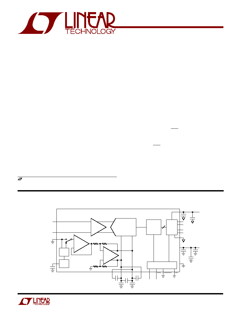
80Msps, 14-Bit ADC with a 2V Differential Input Range
14-BIT
PIPELINED ADC
14
S/H
AMP
±
1V
DIFFERENTIAL
ANALOG INPUT
A
IN
+
A
IN
SENSE
V
CM
4.7
µ
F
DIFF AMP
REFLA
REFHB
GND
1748 BD
ENC
4.7
µ
F
1
µ
F
1
µ
F
0.1
µ
F
0.1
µ
F
REFHA
REFLB
BUFFER
RANGE
SELECT
2.35V
REF
CORRECTION
LOGIC AND
SHIFT
REGISTER
OUTPUT
LATCHES
CONTROL LOGIC
OV
DD
V
DD
OGND
0.5V
TO 5V
5V
0.1
µ
F
1
µ
F
1
µ
F
1
µ
F
D13
D0
CLKOUT
OF
·
·
·
ENC
DIFFERENTIAL
ENCODE INPUT
OE
MSBINV
0.1
µ
F
DESCRIPTIO
U
FEATURES
APPLICATIO S
U
BLOCK DIAGRA
W
2
LTC1748
1748fa
PARAMETER
CONDITIONS
MIN
TYP
MAX
UNITS
Resolution (No Missing Codes)
q
14
Bits
Integral Linearity Error
(Note 6)
3
±
0.75
3
LSB
Differential Linearity Error
q
1
±
0.5
1.5
LSB
Offset Error
(Note 7)
35
±
8
35
mV
Gain Error
External Reference (SENSE = 1.6V)
3.5
±
1
3.5
%FS
Full-Scale Tempco
Internal Reference
±
40
ppm/
°
C
External Reference (SENSE = 1.6V)
±
20
ppm/
°
C
Offset Tempco
±
20
µ
V/
°
C
Input Referred Noise (Transition Noise)
SENSE = 1.6V
0.82
LSB
RMS
ORDER PART
NUMBER
OV
DD
= V
DD
(Notes 1, 2)
Supply Voltage (V
DD
) ............................................. 5.5V
Analog Input Voltage (Note 3) .... 0.3V to (V
DD
+ 0.3V)
Digital Input Voltage (Note 4) ..... 0.3V to (V
DD
+ 0.3V)
Digital Output Voltage ................. 0.3V to (V
DD
+ 0.3V)
OGND Voltage .............................................. 0.3V to 1V
Power Dissipation ............................................ 2000mW
Operating Temperature Range
LTC1748C ............................................... 0
°
C to 70
°
C
LTC1748I ............................................ 40
°
C to 85
°
C
Storage Temperature Range ................. 65
°
C to 150
°
C
Lead Temperature (Soldering, 10 sec).................. 300
°
C
LTC1748CFW
LTC1748IFW
T
JMAX
= 150
°
C,
JA
= 35
°
C/W
The
q
indicates specifications which apply over the full operating
temperature range, otherwise specifications are at T
A
= 25
°
C. (Note 5)
ABSOLUTE
M
AXI
M
U
M
RATINGS
W
W
W
U
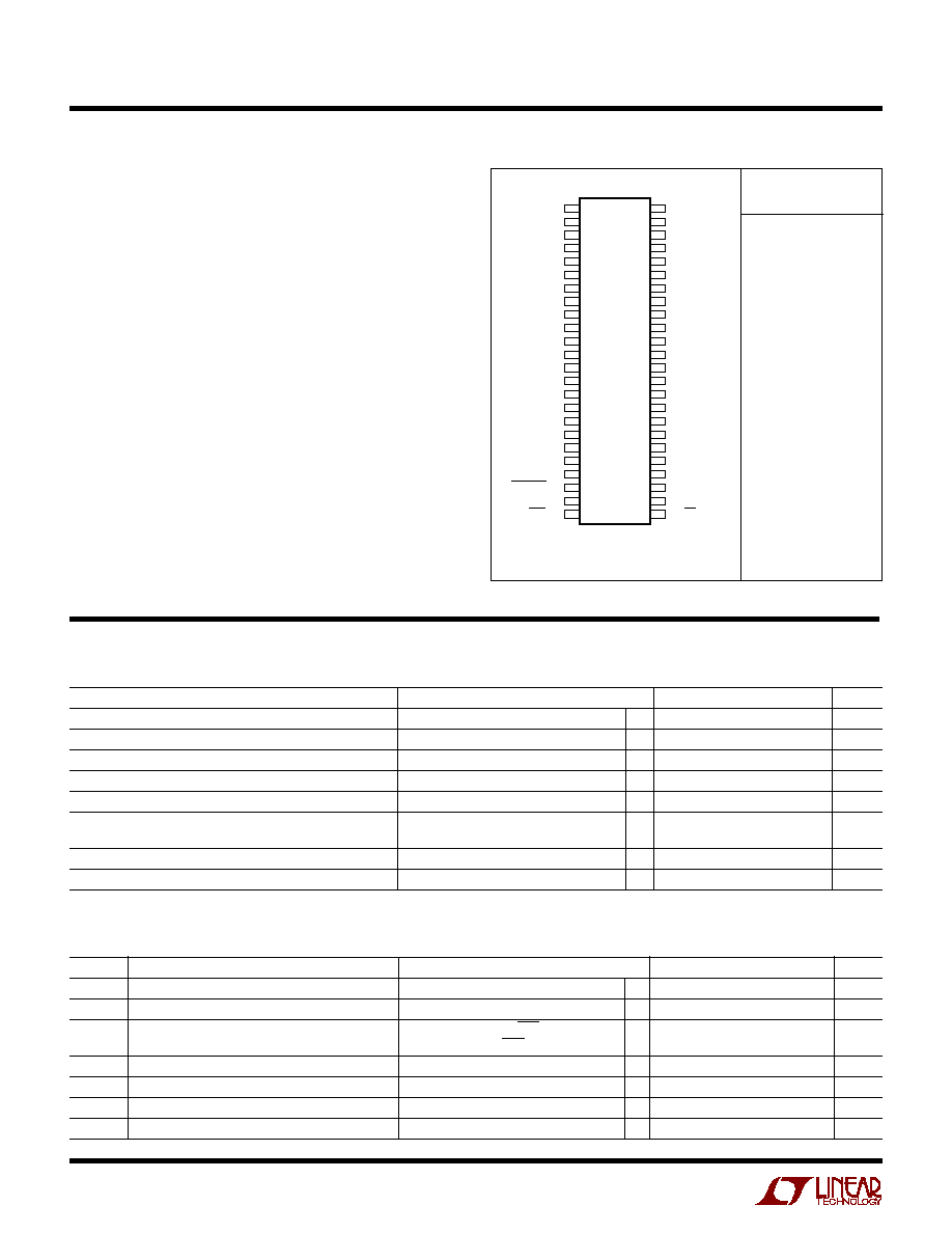
PACKAGE/ORDER I
N
FOR
M
ATIO
N
W
U
U
1
2
3
4
5
6
7
8
9
10
11
12
13
14
15
16
17
18
19
20
21
22
23
24
TOP VIEW
FW PACKAGE
48-LEAD PLASTIC TSSOP
48
47
46
45
44
43
42
41
40
39
38
37
36
35
34
33
32
31
30
29
28
27
26
25
SENSE
V
CM
GND
A
IN
+
A
IN
GND
V
DD
V
DD
GND
REFLB
REFHA
GND
GND
REFLA
REFHB
GND
V
DD
V
DD
GND
V
DD
GND
MSBINV
ENC
ENC
OF
OGND
D13
D12
D11
OV
DD
D10
D9
D8
D7
OGND
GND
GND
D6
D5
D4
OV
DD
D3
D2
D1
D0
OGND
CLKOUT
OE
CO VERTER CHARACTERISTICS
U
SYMBOL
PARAMETER
CONDITIONS
MIN
TYP
MAX
UNITS
V
IN
Analog Input Range (Note 8)
4.75V
V
DD
5.25V
q
±
1 to
±
1.6
V
I
IN
Analog Input Leakage Current
0 < A
IN
+
, A
IN
< V
DD
q
1
1
µ
A
C
IN
Analog Input Capacitance
Sample Mode ENC < ENC
8
pF
Hold Mode ENC > ENC
4
pF
t
ACQ
Sample-and-Hold Acquisition Time
q
5
6
ns
t
AP
Sample-and-Hold Acquisition Delay Time
0
ns
t
JITTER
Sample-and-Hold Acquisition Delay Time Jitter
0.15
ps
RMS
CMRR
Analog Input Common Mode Rejection Ratio
1.5V < (A
IN
= A
IN
+
) < 3V
80
dB
The
q
indicates specifications which apply over the full operating temperature range, otherwise
specifications are at T
A
= 25
°
C. (Note 5)
A ALOG I PUT
U
U
Consult LTC Marketing for parts specified with wider operating temperature ranges.
3
LTC1748
1748fa
PARAMETER
CONDITIONS
MIN
TYP
MAX
UNITS
V
CM
Output Voltage
I
OUT
= 0
2.30
2.35
2.40
V
V
CM
Output Tempco
I
OUT
= 0
±
30
ppm/
°
C
V
CM
Line Regulation
4.75V
V
DD
5.25V
3
mV/V
V
CM
Output Resistance
1mA
I
OUT
1mA
4
(Note 5)
I TER AL REFERE CE CHARACTERISTICS
U
U
U
SYMBOL
PARAMETER
CONDITIONS
MIN
TYP
MAX
UNITS
SNR
Signal-to-Noise Ratio
5MHz Input Signal (2V Range)
72.6
dB
5MHz Input Signal (3.2V Range)
75
76.3
dB
30MHz Input Signal (2V Range)
72.5
dB
30MHz Input Signal (3.2V Range)
74
76.1
dB
70MHz Input Signal (2V Range)
72.2
dB
70MHz Input Signal (3.2V Range)
75.4
dB
140MHz Input Signal (2V Range)
71.4
dB
250MHz Input Signal (2V Range)
68.9
dB
SFDR
Spurious Free Dynamic Range
5MHz Input Signal (2V Range)
90
dB
5MHz Input Signal (3.2V Range) (2nd and 3rd)
90
dB
5MHz Input Signal (3.2V Range) (Other)
94
dB
30MHz Input Signal (2V Range)
90
dB
30MHz Input Signal (3.2V Range) (2nd and 3rd)
80
88
dB
30MHz Input Signal (3.2V Range) (Other)
85
94
dB
70MHz Input Signal (2V Range)
85
dB
70MHz Input Signal (3.2V Range) (2nd and 3rd)
76
dB
70MHz Input Signal (3.2V Range) (Other)
94
dB
140MHz Input Signal (2VRange) (2nd and 3rd)
77
dB
140MHz Input Signal (2V Range) (Other)
93
dB
250MHz Input Signal (2V Range) (2nd and 3rd)
64
dB
250MHz Input Signal (2V Range) (Other)
89
dB
S/(N + D)
Signal-to-(Noise + Distortion) Ratio
5MHz Input Signal (2V Range)
72.4
dB
5MHz Input Signal (3.2V Range)
74.5
76.0
dB
30MHz Input Signal (2V Range)
72.3
dB
30MHz Input Signal (3.2V Range)
75.6
dB
70MHz Input Signal (2V Range)
71
dB
70MHz Input Signal (3.2V Range)
71
dB
THD
Total Harmonic Distortion
5MHz Input Signal, First 5 Harmonics (2V Range)
90
dB
5MHz Input Signal, First 5 Harmonics (3.2V Range)
90
dB
30MHz Input Signal, First 5 Harmonics (2V Range)
90
dB
30MHz Input Signal, First 5 Harmonics (3.2V Range)
85
dB
70MHz Input Signal, First 5 Harmonics (2V Range)
78
dB
70MHz Input Signal, First 5 Harmonics (3.2V Range)
74
dB
IMD
Intermodulation Distortion
f
IN1
= 2.52MHz, f
IN2
= 5.2MHz (2V Range)
97
dBc
f
IN1
= 2.52MHz, f
IN2
= 5.2MHz (3.2V Range)
93
dBc
Sample-and-Hold Bandwidth
R
SOURCE
= 50
240
MHz
T
A
= 25
°
C, A
IN
= 1dBFS (Note 5)
DY
A
IC ACCURACY
U
W
4
LTC1748
1748fa
SYMBOL
PARAMETER
CONDITIONS
MIN
TYP
MAX
UNITS
t
0
ENC Period
(Note 9)
q
12.5
2000
ns
t
1
ENC High
(Note 8)
q
6
1000
ns
t
2
ENC Low
(Note 8)
q
6
1000
ns
t
3
Aperture Delay
(Note 8)
0
ns
t
4
ENC to CLKOUT Falling
C
L
= 10pF (Note 8)
q
1
2.4
4
ns
t
5
ENC to CLKOUT Rising
C
L
= 10pF (Note 8)
t
1
+ t
4
ns
For 80Msps 50% Duty Cycle
C
L
= 10pF (Note 8)
q
7.25
8.65
10.25
ns
t
6
ENC to DATA Delay
C
L
= 10pF (Note 8)
q
2
4.9
7.2
ns
t
7
ENC to DATA Delay (Hold Time)
(Note 8)
q
1.4
3.4
4.7
ns
t
8
ENC to DATA Delay (Setup Time)
C
L
= 10pF (Note 8)
t
0
t
6
ns
For 80Msps 50% Duty Cycle
C
L
= 10pF (Note 8)
q
5.3
7.6
10.5
ns
t
9
CLKOUT to DATA Delay (Hold Time),
(Note 8)
q
6
ns
80Msps 50% Duty Cycle
t
10
CLKOUT to DATA Delay (Setup Time),
C
L
= 10pF (Note 8)
q
2.1
ns
80Msps 50% Duty Cycle
t
11
DATA Access Time After OE
C
L
= 10pF (Note 8)
10
25
ns
t
12
BUS Relinquish
(Note 8)
10
25
ns
Data Latency
5
cycles
The
q
indicates specifications which apply over the full operating temperature
range, otherwise specifications are at T
A
= 25
°
C. (Note 5)
TI I G CHARACTERISTICS
U
W
SYMBOL
PARAMETER
CONDITIONS
MIN
TYP
MAX
UNITS
V
DD
Positive Supply Voltage
4.75
5.25
V
I
DD
Positive Supply Current
q
280
310
mA
P
DIS
Power Dissipation
q
1.4
1.55
W
OV
DD
Digital Output Supply Voltage
0.5
V
DD
V
The
q
indicates specifications which apply over the full operating temperature
range, otherwise specifications are at T
A
= 25
°
C. (Note 5)
POWER REQUIRE E TS
W
U
SYMBOL
PARAMETER
CONDITIONS
MIN
TYP
MAX
UNITS
V
IH
High Level Input Voltage
V
DD
= 5.25V, MSBINV and OE
q
2.4
V
V
IL
Low Level Input Voltage
V
DD
= 4.75V, MSBINV and OE
q
0.8
V
I
IN
Digital Input Current
V
IN
= 0V to V
DD
q
±
10
µ
A
C
IN
Digital Input Capacitance
MSBINV and OE Only
1.5
pF
V
OH
High Level Output Voltage
OV
DD
= 4.75V
I
O
= 10
µ
A
4.74
V
I
O
= 200
µ
A
q
4
4.74
V
V
OL
Low Level Output Voltage
OV
DD
= 4.75V
I
O
= 160
µ
A
0.05
V
I
O
= 1.6mA
q
0.1
0.4
V
I
OZ
Hi-Z Output Leakage D13 to D0
V
OUT
= 0V to V
DD
, OE = High
q
±
10
µ
A
C
OZ
Hi-Z Output Capacitance D13 to D0
OE = High (Note 8)
q
15
pF
I
SOURCE
Output Source Current
V
OUT
= 0V
50
mA
I
SINK
Output Sink Current
V
OUT
= 5V
50
mA
The
q
indicates specifications which apply over the full
operating temperature range, otherwise specifications are at T
A
= 25
°
C. (Note 5)
DIGITAL I PUTS A D DIGITAL OUTPUTS
U
U
5
LTC1748
1748fa
Note 1: Absolute Maximum Ratings are those values beyond which the life
of a device may be impaired.
Note 2: All voltage values are with respect to GND (unless otherwise
noted).
Note 3: When these pin voltages are taken below GND or above V
DD
, they
will be clamped by internal diodes. This product can handle input currents
of greater than 100mA below GND or above V
DD
without latchup.
Note 4: When these pin voltages are taken below GND, they will be
clamped by internal diodes. This product can handle input currents of
>100mA below GND without latchup. These pins are not clamped to V
DD
.
Note 5: V
DD
= 5V, f
SAMPLE
= 80MHz, differential ENC/ENC = 2V
P-P
80MHz
sine wave, input range =
±
1.6V differential, unless otherwise specified.
Note 6: Integral nonlinearity is defined as the deviation of a code from a
straight line passing through the actual endpoints of the transfer curve.
The deviation is measured from the center of the quantization band.
Note 7: Bipolar offset is the offset voltage measured from 0.5 LSB
when the output code flickers between 00 0000 0000 0000 and 11
1111 1111 1111.
Note 8: Guaranteed by design, not subject to test.
Note 9: Recommended operating conditions.
ELECTRICAL CHARACTERISTICS
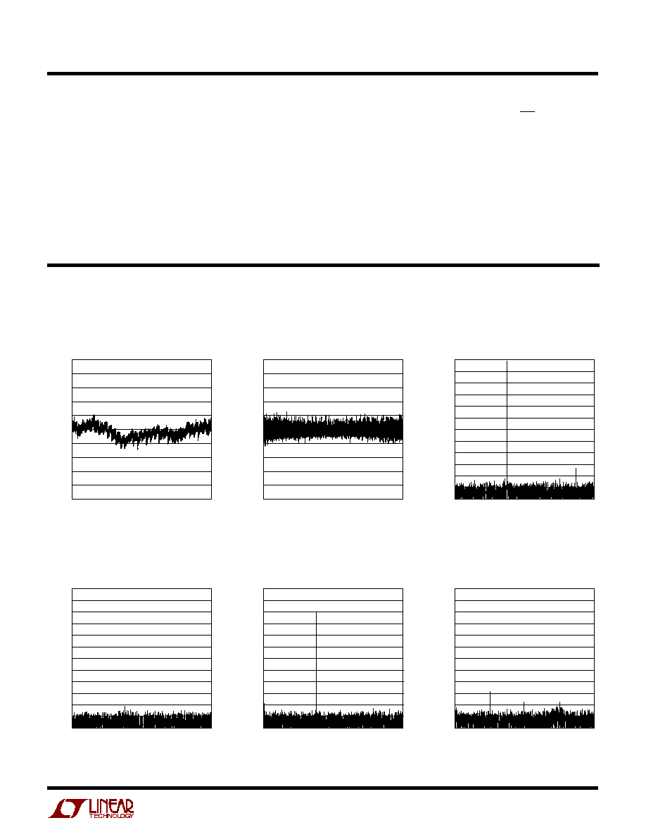
TYPICAL PERFOR A CE CHARACTERISTICS
U
W
INL, 3.2V Range
DNL, 3.2V Range
8192 Point FFT,
Input Frequency = 15.068MHz,
1dB, 3.2V Range
FREQUENCY (MHz)
0
AMPLITUDE (dBFS)
60
30
20
40
1748 G03
70
80
120
10
20
30
5
15
25
35
100
0
10
40
50
90
110
T
A
= 25
°
C
8192 Point FFT,
Input Frequency = 15.068MHz,
10dB, 3.2V Range
FREQUENCY (MHz)
0
AMPLITUDE (dBFS)
60
30
20
40
1748 G04
70
80
120
10
20
30
5
15
25
35
100
0
10
40
50
90
110
T
A
= 25
°
C
8192 Point FFT,
Input Frequency = 15.068MHz,
20dB, 3.2V Range
FREQUENCY (MHz)
0
AMPLITUDE (dBFS)
60
30
20
40
1748 G05
70
80
120
10
20
30
5
15
25
35
100
0
10
40
50
90
110
T
A
= 25
°
C
8192 Point FFT,
Input Frequency = 30.068MHz,
1dB, 3.2V Range
FREQUENCY (MHz)
0
AMPLITUDE (dBFS)
60
30
20
40
1748 G06
70
80
120
10
20
30
5
15
25
35
100
0
10
40
50
90
110
T
A
= 25
°
C
OUTPUT CODE
0
2.5
ERROR (LSB)
2.0
1.0
0.5
0
2.5
T
A
= 25
°
C
1.0
4096
8192
1748 G01
1.5
1.5
2.0
0.5
12288
16384
OUTPUT CODE
0
1.0
ERROR (LSB)
0.8
0.4
0.2
0
1.0
0.4
4096
8192
1748 G02
0.6
0.6
0.8
0.2
12288
16384
T
A
= 25
°
C