 | ÐлекÑÑоннÑй компоненÑ: LTC1871-7 | СкаÑаÑÑ:  PDF PDF  ZIP ZIP |
1871i.pm65
1
LTC1871-7
18717i
FEATURES
APPLICATIO S
U
TYPICAL APPLICATIO
U
High Input Voltage,
Current Mode Boost,
Flyback and SEPIC Controller
July 2002
The LTC
®
1871-7 is a current mode, boost, flyback and
SEPIC controller optimized for driving 6V-rated MOSFETs
in high voltage applications. The LTC1871-7 works equally
well in low or high power applications and requires few
components to provide a complete power supply solu-
tion. The switching frequency can be set with an external
resistor over a 50kHz to 1MHz range, and can be synchro-
nized to an external clock using the MODE/SYNC pin.
Burst Mode operation at light loads, a low minimum
operating supply voltage of 6V and a low shutdown
quiescent current of 10
µ
A make the LTC1871-7 well
suited for battery-operated systems. For applications
requiring constant frequency operation, Burst Mode op-
eration can be defeated using the MODE/SYNC pin. The
LTC1871-7 is available in the 10-lead MSOP package.
s
Optimized for High Input Voltage Applications
s
Wide Chip Supply Voltage Range: 6V to 36V
s
Internal 7V Low Dropout Voltage Regulator
Optimized for 6V-Rated MOSFETs
s
Current Mode Control Provides Excellent
Transient Response
s
High Maximum Duty Cycle (92% Typ)
s
±
2% RUN Pin Threshold with 100mV Hysteresis
s
±
1% Internal Voltage Reference
s
Micropower Shutdown: I
Q
= 10
µ
A
s
Programmable Operating Frequency
(50kHz to 1MHz) with One External Resistor
s
Synchronizable to an External Clock Up to 1.3
×
f
OSC
s
User-Controlled Pulse Skip or Burst Mode
®
Operation
s
Output Overvoltage Protection
s
Can be Used in a No R
SENSE
TM
Mode for V
DS
< 36V
s
Small 10-Lead MSOP Package
s
Telecom Power Supplies
s
42V Automotive Systems
s
24V Industrial Controls
s
IP Phone Power Supplies
Burst Mode is a registered trademark of Linear Technology Corporation.
No R
SENSE
is a trademark of Linear Technology Corporation.
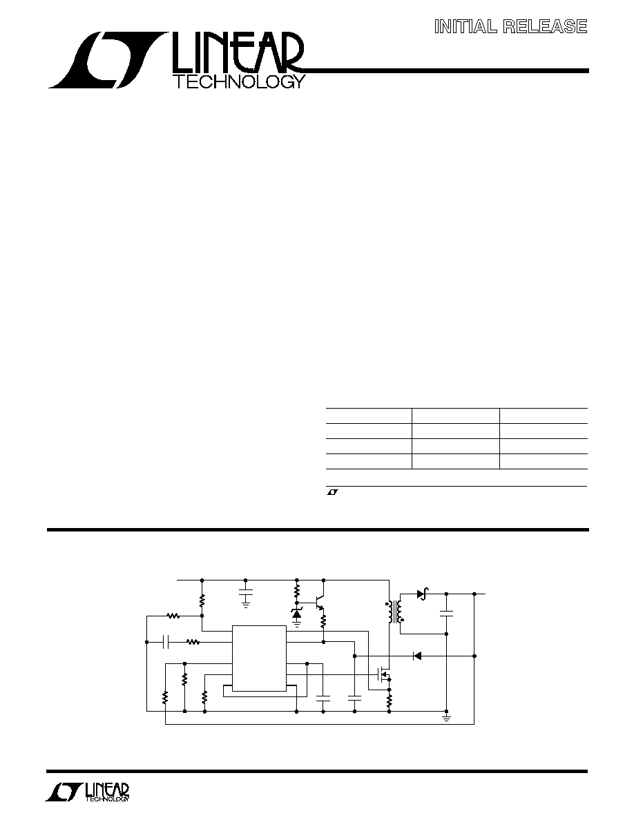
Figure 1. Small, Nonisolated 12V Flyback Telecom Housekeeping Supply
, LTC and LT are registered trademarks of Linear Technology Corporation.
Information furnished by Linear Technology Corporation is believed to be accurate and reliable.
However, no responsibility is assumed for its use. Linear Technology Corporation makes no represen-
tation that the interconnection of its circuits as described herein will not infringe on existing patent rights.
DESCRIPTIO
U
RUN
I
TH
FB
FREQ
MODE/SYNC
SENSE
V
IN
INTV
CC
GATE
GND
LTC1871-7
120k
4.7
µ
F
X5R
2.2
µ
F
100V
X7R
M1
FDC2512
0.12
V
IN
36V TO 72V
3.4k
2.2nF
26.7k
D3
10BQ060
47
µ
F
16V
X5R
V
OUT
12V
0.4A
604k
12.4k
T1
VP1-0076
100k
10
Q1
FMMT625
D2
4148
D1
9.1V
110k
0.1
µ
F
X5R
3:1
18717 F01
PARAMETER
LTC1871-7
LTC1871
INTV
CC
7.0V
5.2V
INTV
CC
UV
+
5.6V
2.1V
INTV
CC
UV
4.6V
1.9V
Final Electrical Specifications
2
LTC1871-7
18717i
(Note 1)
V
IN
Voltage ............................................... 0.3V to 36V
INTV
CC
Voltage ........................................... 0.3V to 9V
INTV
CC
Output Current ........................................ 50mA
GATE Voltage ........................... 0.3V to V
INTVCC
+ 0.3V
I
TH
, FB Voltages ....................................... 0.3V to 2.7V
RUN Voltage ............................................... 0.3V to 7V
MODE/SYNC Voltage ................................... 0.3V to 9V
FREQ Voltage ............................................ 0.3V to 1.5V
SENSE Pin Voltage ................................... 0.3V to 36V
Operating Temperature Range (Note 2) .. 40
°
C to 85
°
C
Junction Temperature (Note 3) ............................ 125
°
C
Storage Temperature Range ................. 65
°
C to 150
°
C
Lead Temperature (Soldering, 10 sec).................. 300
°
C
ORDER PART
NUMBER
LTC1871EMS-7
T
JMAX
= 125
°
C,
JA
= 120
°
C/ W
ABSOLUTE AXI U RATI GS
W
W
W
U
PACKAGE/ORDER I FOR ATIO
U
U
W
ELECTRICAL CHARACTERISTICS
MS PART MARKING
LTG4
1
2
3
4
5
RUN
I
TH
FB
FREQ
MODE/
SYNC
10
9
8
7
6
SENSE
V
IN
INTV
CC
GATE
GND
TOP VIEW
MS PACKAGE
10-LEAD PLASTIC MSOP
SYMBOL
PARAMETER
CONDITIONS
MIN
TYP
MAX
UNITS
Main Control Loop
V
IN(MIN)
Minimum Input Voltage
6
V
I
Q
Input Voltage Supply Current
(Note 4)
Continuous Mode
V
MODE/SYNC
= 5V, V
FB
= 1.4V, V
ITH
= 0.75V
600
1000
µ
A
Burst Mode Operation, No Load
V
MODE/SYNC
= 0V, V
ITH
= 0.2V (Note 5)
280
500
µ
A
Shutdown Mode
V
RUN
= 0V
12
25
µ
A
V
RUN
+
Rising RUN Input Threshold Voltage
1.348
V
V
RUN
Falling RUN Input Threshold Voltage
1.223
1.248
1.273
V
q
1.198
1.298
V
V
RUN(HYST)
RUN Pin Input Threshold Hysteresis
50
100
150
mV
I
RUN
RUN Input Current
5
60
nA
V
FB
Feedback Voltage
V
ITH
= 0.2V (Note 5)
1.218
1.230
1.242
V
q
1.212
1.248
V
I
FB
FB Pin Input Current
V
ITH
= 0.2V (Note 5)
18
60
nA
V
FB
Line Regulation
6V
V
IN
30V
0.002
0.02
%/V
V
IN
V
FB
Load Regulation
V
MODE/SYNC
= 0V, V
TH
= 0.5V to 0.90V (Note 5)
q
1
0.1
%
V
ITH
V
FB(OV)
FB Pin, Overvoltage Lockout
V
FB(OV)
V
FB(NOM)
in Percent
2.5
6
10
%
g
m
Error Amplifier Transconductance
I
TH
Pin Load =
±
5
µ
A (Note 5)
600
µ
mho
V
ITH(BURST)
Burst Mode Operation I
TH
Pin Voltage
Falling I
TH
Voltage (Note 5)
0.3
V
V
SENSE(MAX)
Maximum Current Sense Input Threshold
Duty Cycle < 20%
120
150
180
mV
I
SENSE(ON)
SENSE Pin Current (GATE High)
V
SENSE
= 0V
35
70
µ
A
I
SENSE(OFF)
SENSE Pin Current (GATE Low)
V
SENSE
= 30V (No R
SENSE
Mode)
0.1
5
µ
A
The
q
denotes specifications which apply over the full operating temperature range, otherwise specifications are at T
A
= 25
°
C.
V
IN
= 8V, V
RUN
= 1.5V, R
FREQ
= 80k, V
MODE/SYNC
= 0V, unless otherwise specified.
Consult LTC Marketing for parts specified with wider operating temperature ranges.
3
LTC1871-7
18717i
ELECTRICAL CHARACTERISTICS
Note 1: Absolute Maximum Ratings are those values beyond which the life
of the device may be impaired.
Note 2: The LTC1871-7E is guaranteed to meet performance specifications
from 0
°
C to 70
°
C. Specifications over the 40
°
C to 85
°
C operating
temperature range are assured by design, characterization and correlation
with statistical process controls.
Note 3: T
J
is calculated from the ambient temperature T
A
and power
dissipation P
D
according to the following formula:
T
J
= T
A
+ (P
D
· 120
°
C/W)
Note 4: The dynamic input supply current is higher due to power MOSFET
gate charging (Q
G
· f
OSC
). See Applications Information.
Note 5: The LTC1871-7 is tested in a feedback loop that servos V
FB
to the
reference voltage with the I
TH
pin forced to a voltage between 0V and 1.4V
(the no load to full load operating voltage range for the I
TH
pin is 0.3V to
1.23V).
Note 6: In a synchronized application, the internal slope compensation
gain is increased by 25%. Synchronizing to a significantly higher ratio will
reduce the effective amount of slope compensation, which could result in
subharmonic oscillation for duty cycles greater than 50%.
Note 7: Rise and fall times are measured at 10% and 90% levels.
The
q
denotes specifications which apply over the full operating temperature range, otherwise specifications are at T
A
= 25
°
C.
V
IN
= 8V, V
RUN
= 1.5V, R
FREQ
= 80k, V
MODE/SYNC
= 0V, unless otherwise specified.
SYMBOL
PARAMETER
CONDITIONS
MIN
TYP
MAX
UNITS
Oscillator
f
OSC
Oscillator Frequency
R
FREQ
= 80k
250
300
350
kHz
Oscillator Frequency Range
50
1000
kHz
D
MAX
Maximum Duty Cycle
87
92
97
%
f
SYNC/
f
OSC
Recommended Maximum Synchronized
f
OSC
= 300kHz (Note 6)
1.25
1.30
Frequency Ratio
t
SYNC(MIN)
MODE/SYNC Minimum Input Pulse Width
V
SYNC
= 0V to 5V
25
ns
t
SYNC(MAX)
MODE/SYNC Maximum Input Pulse Width
V
SYNC
= 0V to 5V
0.8/f
OSC
ns
V
IL(MODE)
Low Level MODE/SYNC Input Voltage
0.3
V
V
IH(MODE)
High Level MODE/SYNC Input Voltage
1.2
V
R
MODE/SYNC
MODE/SYNC Input Pull-Down Resistance
50
k
V
FREQ
Nominal FREQ Pin Voltage
0.62
V
Low Dropout Regulator
V
INTVCC
INTV
CC
Regulator Output Voltage
V
IN
= 8V
6.5
7
7.5
V
UVLO
INTV
CC
Undervoltage Lockout Thresholds
Rising INTV
CC
5.6
V
Falling INTV
CC
4.6
V
UVLO Hysteresis
1.0
V
V
INTVCC
INTV
CC
Regulator Line Regulation
8V
V
IN
15V
8
25
mV
V
IN1
V
INTVCC
INTV
CC
Regulator Line Regulation
15V
V
IN
30V
70
200
mV
V
IN2
V
LDO(LOAD)
INTV
CC
Load Regulation
0
I
INTVCC
20mA, V
IN
= 8V
2
0.2
%
V
DROPOUT
INTV
CC
Regulator Dropout Voltage
V
IN
= 6V, INTV
CC
Load = 20mA
280
mV
GATE Driver
t
r
GATE Driver Output Rise Time
C
L
= 3300pF (Note 7)
17
100
ns
t
f
GATE Driver Output Fall Time
C
L
= 3300pF (Note 7)
8
100
ns
4
LTC1871-7
18717i
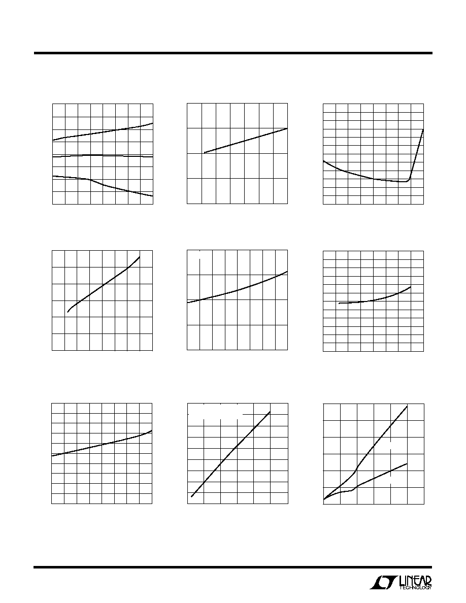
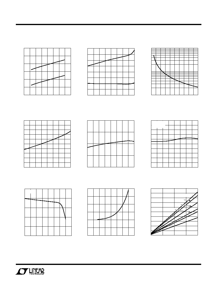
TYPICAL PERFOR A CE CHARACTERISTICS
U
W
FB Voltage vs Temp
FB Voltage Line Regulation
FB Pin Current vs Temperature
TEMPERATURE (
°
C)
50
FB VOLTAGE (V)
1.23
1.24
150
1871 G01
1.22
1.21
0
50
100
25
25
75
125
1.25
V
IN
(V)
0
1.229
FB VOLTAGE (V)
1.230
1.231
5
10
15
20
1871 G02
25
30
35
TEMPERATURE (
°
C)
50
0
FB PIN CURRENT (nA)
10
20
30
40
60
25
25
0
50
100
75
1871 G03
125 150
50
Shutdown Mode I
Q
vs V
IN
Burst Mode I
Q
vs V
IN
V
IN
(V)
0
0
SHUTDOWN MODE I
Q
(
µ
A)
10
20
10
20
30
40
1871 G04
30
Shutdown Mode I
Q
vs Temperature
TEMPERATURE (
°
C)
50
0
SHUTDOWN MODE I
Q
(
µ
A)
5
10
15
20
25
0
25
50
1871 G05
75
100 125 150
V
IN
= 8V
V
IN
(V)
0
0
Burst Mode I
Q
(
µ
A)
100
200
300
400
600
10
20
1871 G06
30
40
500
Burst Mode I
Q
vs Temperature
Gate Drive Rise and Fall Time
vs C
L
Dynamic I
Q
vs Frequency
TEMPERATURE (
°
C)
50
0
Burst Mode I
Q
(
µ
A)
200
500
0
50
75
1871 G07
100
400
300
25
25
100 125
150
FREQUENCY (kHz)
0
0
I
Q
(mA)
2
6
8
10
800
18
1871 G08
4
400
1200
600
200
1000
12
14
16
C
L
= 3300pF
I
Q(TOT)
= 600
µ
A + Qg · f
C
L
(pF)
0
0
TIME (ns)
10
20
30
40
60
2000
4000
6000
8000
1871 G09
10000 12000
50
RISE TIME
FALL TIME
5
LTC1871-7
18717i
TYPICAL PERFOR A CE CHARACTERISTICS
U
W
RUN Thresholds vs V
IN
R
T
vs Frequency
Frequency vs Temperature
SENSE Pin Current vs Temperature
Maximum Sense Threshold
vs Temperature
INTV
CC
Load Regulation
INTV
CC
Dropout Voltage
vs Current, Temperature
INTV
CC
Line Regulation
V
IN
(V)
0
1.2
RUN THRESHOLDS (V)
1.3
1.4
10
20
30
40
1871 G10
1.5
RUN Thresholds vs Temperature
TEMPERATURE (
°
C)
50
RUN THRESHOLDS (V)
1.30
1.35
150
1871 G11
1.25
1.20
0
50
100
25
25
75
125
1.40
FREQUENCY (kHz)
100
R
T
(k
)
300
1000
1871 G12
10
100
200
1000
900
800
700
600
500
400
0
TEMPERATURE (
°
C)
50
275
GATE FREQUENCY (kHz)
280
290
295
300
325
310
0
50
75
1871 G13
285
315
320
305
25
25
100 125
150
TEMPERATURE (
°
C)
50
140
MAX SENSE THRESHOLD (mV)
145
150
155
160
25
0
25
50
1871 G14
75
100 125 150
TEMPERATURE (
°
C)
50
25
SENSE PIN CURRENT (
µ
A)
30
35
0
50
75
1871 G15
25
25
100 125
150
GATE HIGH
V
SENSE
= 0V
INTV
CC
LOAD (mA)
0
INTV
CC
VOLTAGE (V)
7.0
30
50
80
1871 G16
6.9
6.8
10
20
40
60
70
V
IN
= 8V
V
IN
(V)
0
6.9
INTV
CC
VOLTAGE (V)
7.0
7.1
10
20
30
40
1871 G17
7.2
5
15
25
35
INTV
CC
LOAD (mA)
0
0
DROPOUT VOLTAGE (mV)
50
150
200
250
500
350
5
10
1871 G18
100
400
450
300
15
20
150
°
C
75
°
C
125
°
C
25
°
C
50
°
C
0
°
C